Paper Sharing
【Member Papers】Influence of dislocation clusters on homoepitaxial layers grown by halide vap-or phase epitaxy (001) β-Ga₂O₃ investigated by synchrotron x-ray topography and scanning transmission electron microscopy
日期:2026-05-18阅读:4
Researchers from Novel Crystal Technology, Inc. have published a dissertation titled " Influence of dislocation clusters on homoepitaxial layers grown by halide vapor phase epitaxy (001) β-Ga2O3 investigated by synchrotron x-ray topography and scanning transmission electron microscopy " in Applied Physics Letters.
Background
Beta-gallium oxide (β-Ga2O3) demonstrates a wide bandgap of ~4.8eV and a high breakdown field of 8 MV/cm, making it a promising material for the next-generation power device application. Additionally, β-Ga2O3 single crystal can be easily produced at a high growth rate by using melt-growth techniques such as edge-defined film-fed growth (EFG), floating zone, Czochralski, and vertical Bridgeman. Large-size (4-in.) (001) β-Ga2O3 EFG substrates have already been commercially available. The electron concentration in β-Ga2O3 can be achieved in a wide range from 1016 to 1019 cm−3 by doping with Sn or Si. These advantages have driven the rapid development of β-Ga2O3-based power devices, particularly vertical devices, which have emerged as a key area of research. At present, the commercial production of β-Ga2O3 epitaxial wafers for these power devices predominantly rely on the halide vapor phase epitaxy (HVPE) technique on the (001) substrate owing to the availability of large-size wafers in this orientation and its relatively high growth rate of approximately 5um/h compared with other orientations such as (011) (2.8 um/h) and (-102) (4.2 um/h). The differences in growth rate could have arisen from variations in surface energy and bonding configurations for each crystallographic orientation. However, deep pits are commonly observed following the HVPE growth on (001) β-Ga2O3, which can potentially harm the devices’ performance. These pits have a depth of ~40% of the film thickness and must be removed prior to device fabrication using the chemical mechanical polishing (CMP) process, which significantly drives up the production costs. Understanding the origin of these pits is, therefore, essential to eliminate them from the epitaxial layer and enhance device performance. However, the origins of these pits remain largely unexplored, hindering a comprehensive understanding of their formation mechanisms and limiting the development of effective strategies for their mitigation during the epitaxial growth.
Abstract
Pit formation on the as-grown halide vapor phase epitaxy (001) β-Ga2O3 surface was primarily attributed to dislocation clusters in the substrate. Cross-sectional x-ray topography showed that these clusters penetrate to a minimum measured depths of roughly 210um below the (001) surface. Etch pit formation of the dislocation cluster revealed a distinctive type of etch pits, where the main etch pits are accompanied by smaller etch pits aligned at angles of approximately ±38° relative to the [010] direction near the head of primary etch pit. Further analysis by cross-sectional scanning electron microscopy observation confirmed that these smaller pits arise from (-1-0-25) and (-1-025) stacking faults, which are speculated to serve as propagation paths for the dislocation clusters.
Conclusion
In conclusion, dislocation clusters present in the substrate were identified as the primary cause of the pits’ formation on the as-grown HVPE (001) β-Ga2O3 surface. The dislocation clusters extended up to the depth of ~210um beneath the (001) surface as examined by cross-sectional XRT observation. Etch pit formation revealed a particular type of etch pit that is accompanied by small etch pits arranged at angles of approximately ±38° relative to the [010] direction near the head region of the primary etch pits. These small pits were later confirmed to originate from the (-1-0-25) and (-1-025) SFs, along which the dislocation clusters are speculated to propagate.
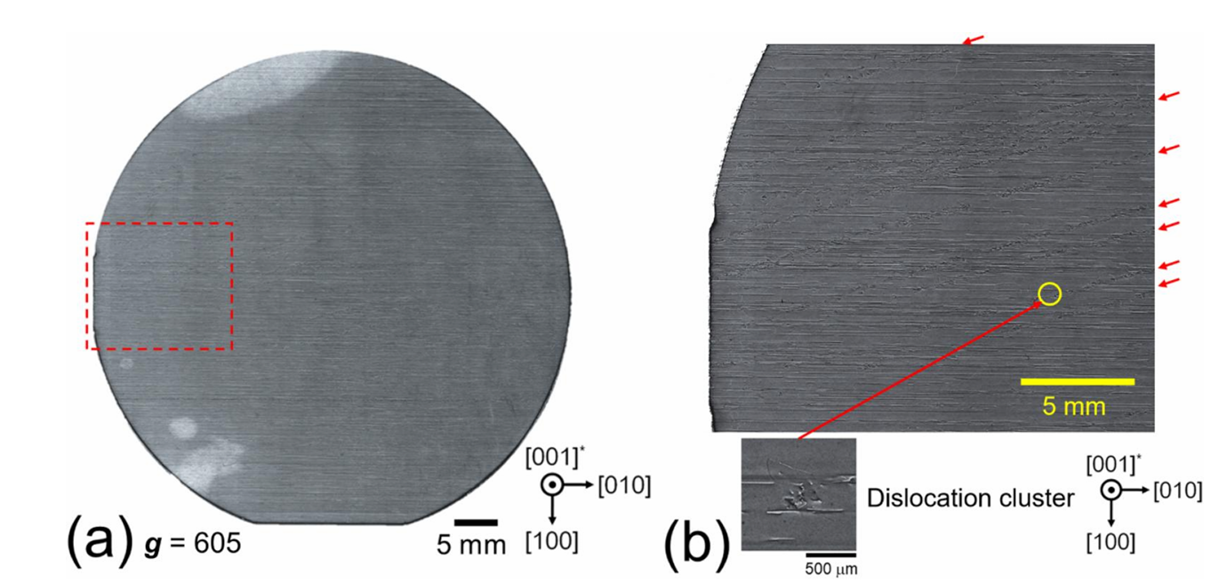
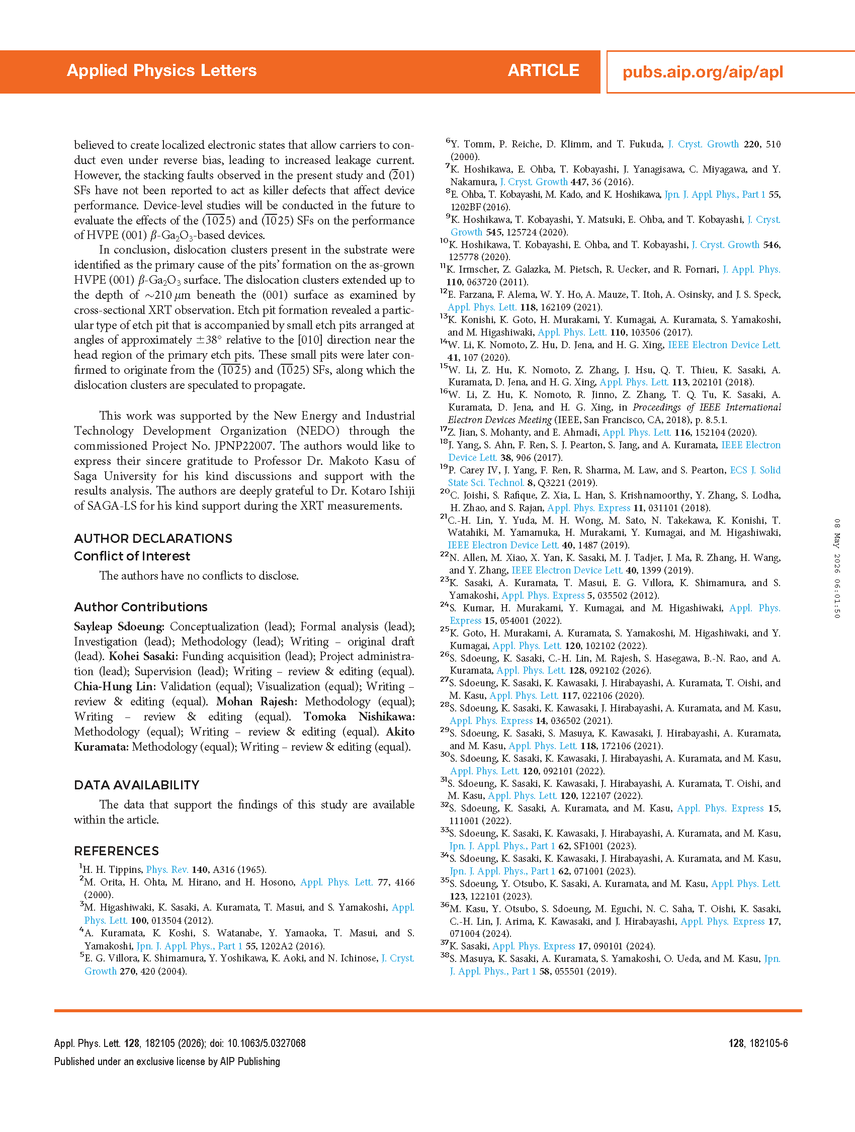
FIG. 1. (a) and (b) show the synchrotron XRT image of the 2-in. substrate taken under the diffraction condition g = 6 0 5 and its enlarged image of the outline region, respectively. The dislocation clusters are indicated by red arrows.
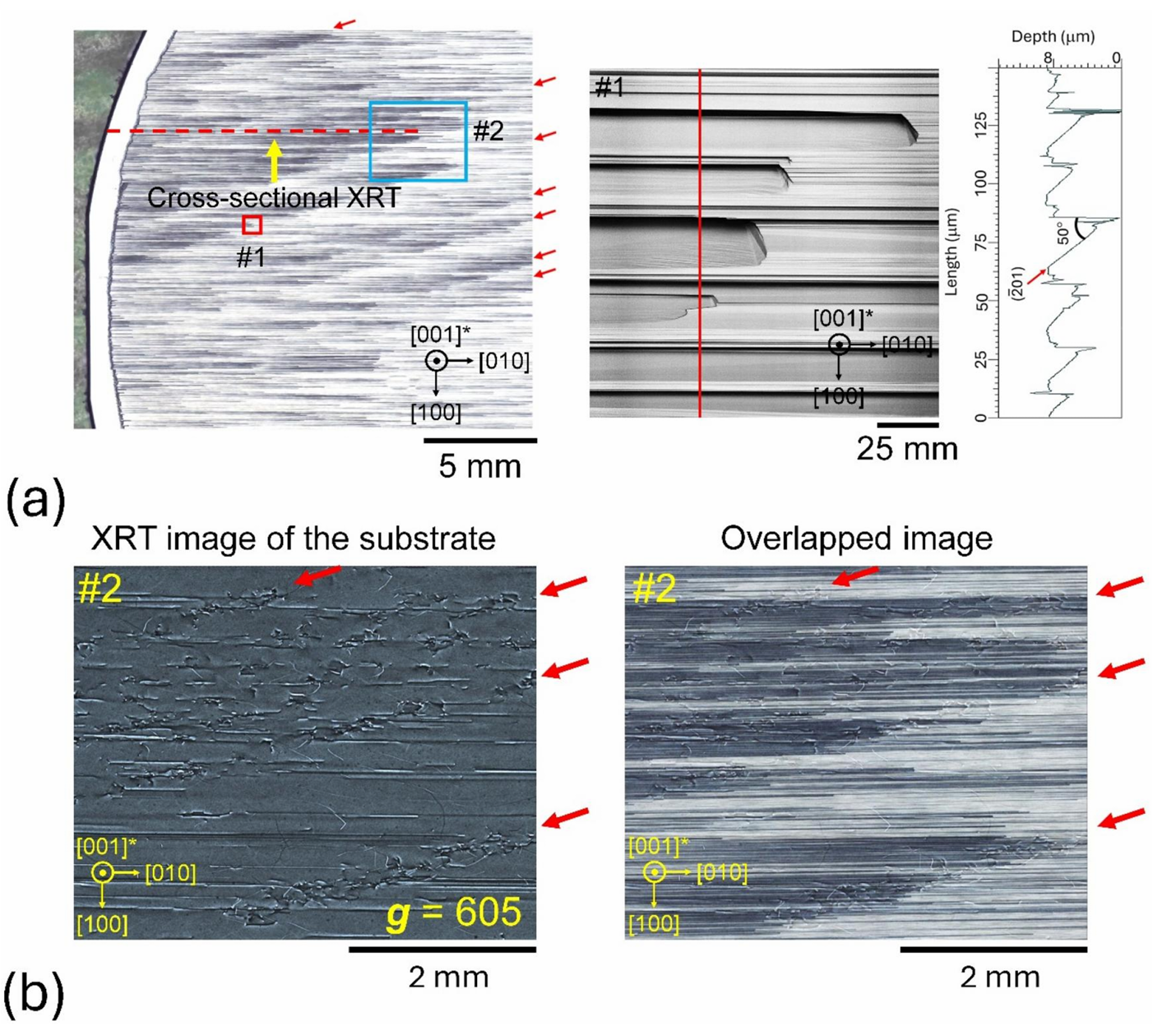
FIG. 2. (a) Confocal microscopy image of the as-grown HVPE surface captured at the same location as Fig. 1(b), along with its high-magnification view of #1 position and (b) enlarged XRT image of the substrate at #2 with the overlapped image with the as-grown HVPE surface. The dislocation clusters and pits on the as-grown HVPE surface are indicated by red arrows.
FIG. 3. (a) Cross-sectional XRT image at the red dashed line position in Fig. 2(a) taken with the g of 12 2 0 and (b) its enlarged images from #1 to #5.
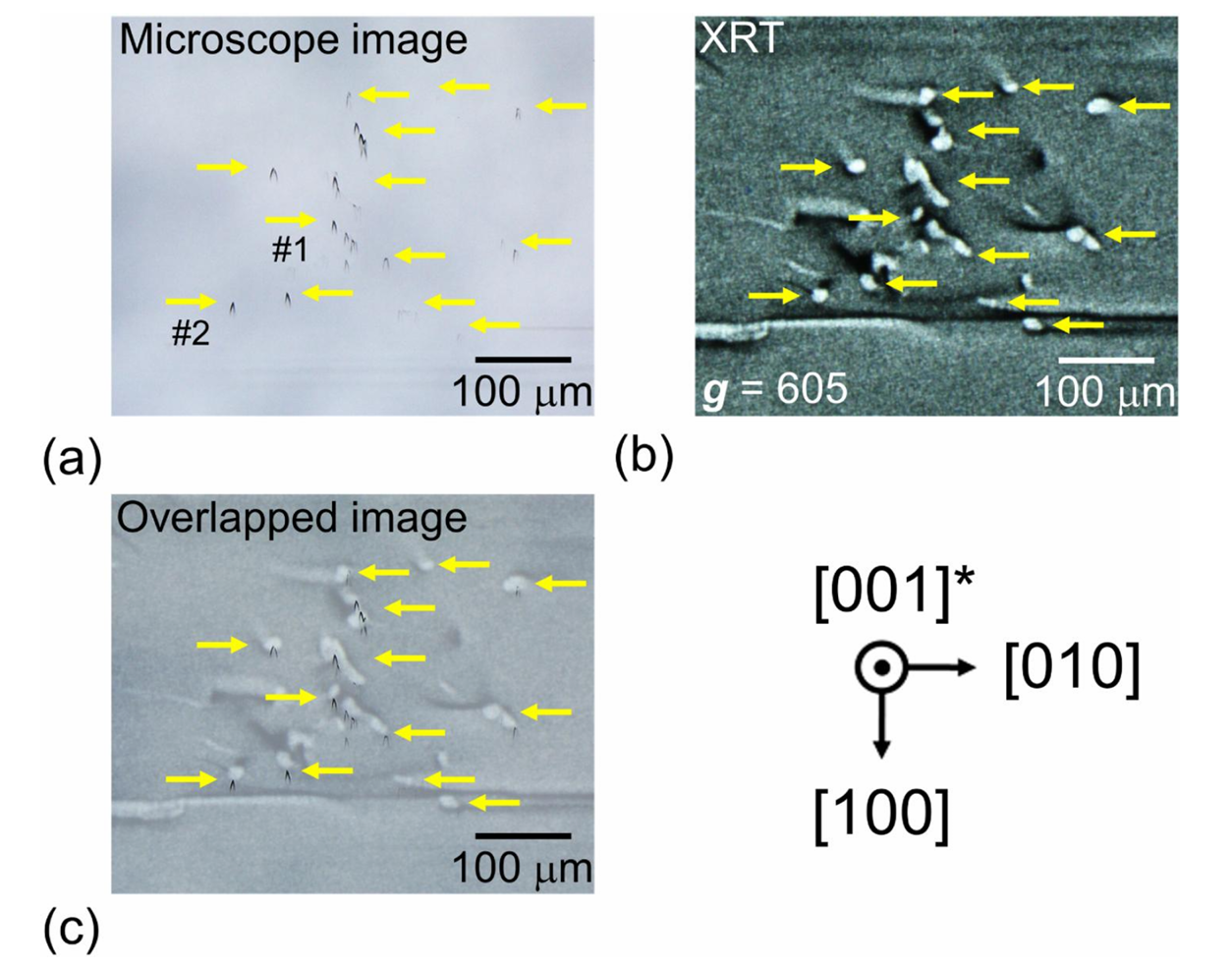
FIG. 4. (a) Microscope image of the etch pits at the dislocation cluster region, (b) its corresponding XRT image taken by the g of 6 0 5, and (c) the overlapped image of (a) and (b).
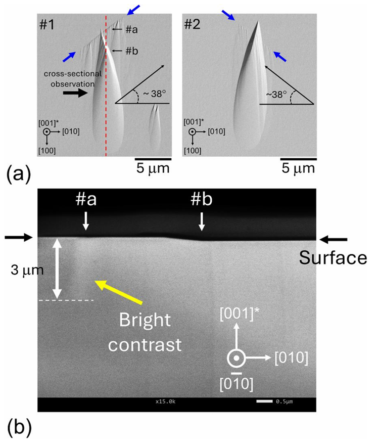
FIG. 5. (a) and (b) SEM image of etch pits #1 and #2 and the cross-sectional SEM image of the etch pit #1, respectively.
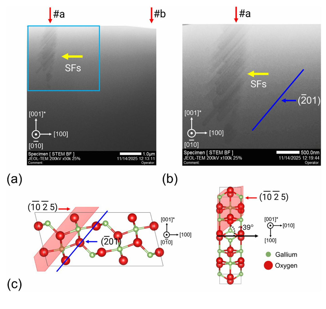
FIG. 6. (a) Low-magnification STEM image of etch pit #1, (b) enlarged STEM image of the outline region, and (c) unit cell of β-Ga2O3 drawn by VESTA.
DOI:
doi.org/10.1063/5.0327068