Paper Sharing
【Member Papers】High-performance HfO₂ dielectric gated Ge-doped κ-Ga₂O₃ thin-film transistors
日期:2026-05-15阅读:23
Researchers from Hubei University, Wuhan Textile University and Austrian Academy of Sciences have published an article titled “High-performance HfO₂ dielectric gated Ge-doped κ-Ga₂O₃ thin-film transistors” in Applied Physics Letters.
Background
κ-Ga₂O₃ is a highly promising ultra-wide bandgap semiconductor for next-generation power electronics and thin-film transistors due to its spontaneous polarization and high breakdown field. Conventional Si and Sn doping easily induce lattice distortion, and heteroepitaxy on regular c-plane sapphire tends to generate in-plane rotational domains and grain boundaries, which significantly degrade mobility. Meanwhile, traditional gate dielectrics exhibit weak electrostatic control, making it difficult to achieve high on/off ratio and enhancement-mode operation, thus limiting the development of high-performance κ-Ga₂O₃ transistors. At present, studies on integrating Ge doping for phase stabilization, off-cut substrates for epitaxy quality improvement, and HfO₂ high-k dielectric for enhanced gate control are still insufficient, and no reproducible strategy for high-performance enhancement-mode transistors has been established.
Abstract
Orthorhombic κ-Ga₂O₃ has emerged as a promising candidate for next-generation power electronics due to its ultra-wide bandgap and high breakdown field. Herein, Ge-doped Ga₂O₃ thin films were grown via pulsed laser deposition as active channels on c-sapphire, 6° off-axis c-sapphire (6°/c-sapphire), and MgO (100) substrates to explore thin-film transistors (TFTs). Ge was strategically introduced to stabilize the κ-phase and control carrier concentrations in the range of 10¹⁶–10¹⁷ cm⁻³. Top-gate TFTs were fabricated utilizing HfO₂ as the high-k gate dielectric and Ti/Au as source/drain Ohmic contacts. Structural analyses indicate that substrate choice is critical: MgO(100) favors β-Ga₂O₃, while sapphire promotes κ-Ga₂O₃. Notably, the 6°/c-sapphire substrates yielded smooth films with minimal defects, which achieved an optimal carrier concentration (3.98 ×10¹⁷ cm⁻³) and a peak Hall mobility of 3.95 cm² V⁻¹ s⁻¹. Corresponding TFTs exhibited superior enhancement-mode characteristics with a threshold voltage of 2.6 V, subthreshold swing of 1.48 V/dec, and a high current on/off ratio of 7.16 × 10⁵. Technology-computer-aided-design simulations suggest a theoretical breakdown voltage of 298 V, limited primarily by gate-edge field crowding. This work demonstrates that synergistic strategy of Ge doping and 6°/c-sapphire substrate use can lead to high-quality κ-phase Ga₂O₃:Ge for high-performance power electronics.
Highlights
Realize high-performance enhancement-mode κ-Ga₂O₃:Ge thin-film transistors by Ge doping and 6° off-axis sapphire substrate.
Achieve phase stabilization of κ-Ga₂O₃ and carrier concentration modulation via Ge doping.
Obtain low-defect, smooth κ-Ga₂O₃:Ge films on 6°/c-sapphire with improved mobility.
Demonstrate top-gate TFTs with high current on/off ratio of 7.16 ×10⁵ and threshold voltage of 2.6 V.
Reveal breakdown mechanism dominated by gate-edge electric field crowding via TCAD simulation.
Conclusion
In conclusion, this work systematically investigates the structural and electrical properties of Ga₂O₃:Ge thin films across three distinct substrates, profoundly elucidating the decisive role of heteroepitaxial substrate engineering in modulating the performance of ultra-wide bandgap semiconductor devices. The results demonstrate that κ-Ga₂O₃:Ge films grown on 6°/c-sapphire exhibit enhanced surface planarity and superior carrier mobility. Evaluation of the 6°/c-sapphire-based devices reveals significant performance leaps, which achieve a high μsat of 13.7 cm² V⁻¹ s⁻¹ and an impressive Ion/Ioff of 7.16 ×10⁵. While the observed SS remains relatively high, it presents a clear pathway for further optimization through refined interface engineering. This study presents a simple and effective method to enhance the mobility and overall performance of κ-Ga₂O₃ TFTs by the introduction of Ge as dopant and 6°/c-sapphire as template for Ga₂O₃.
Project Support
This work was supported by the National Natural Science Foundation of China (Grant Nos. 62274057, 11975093, and 52202132), the Sino-German Mobility Program (Grant No. M-0764), the Hubei International Science and Technology Cooperation Project (Grant No. 2025EHA006), and the Wuhan Municipal Bureau of Science and Technology Innovation (Grant Nos. 2024040801020306 and 2025011202030396).
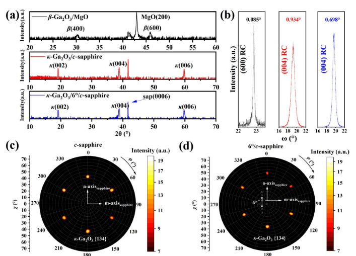
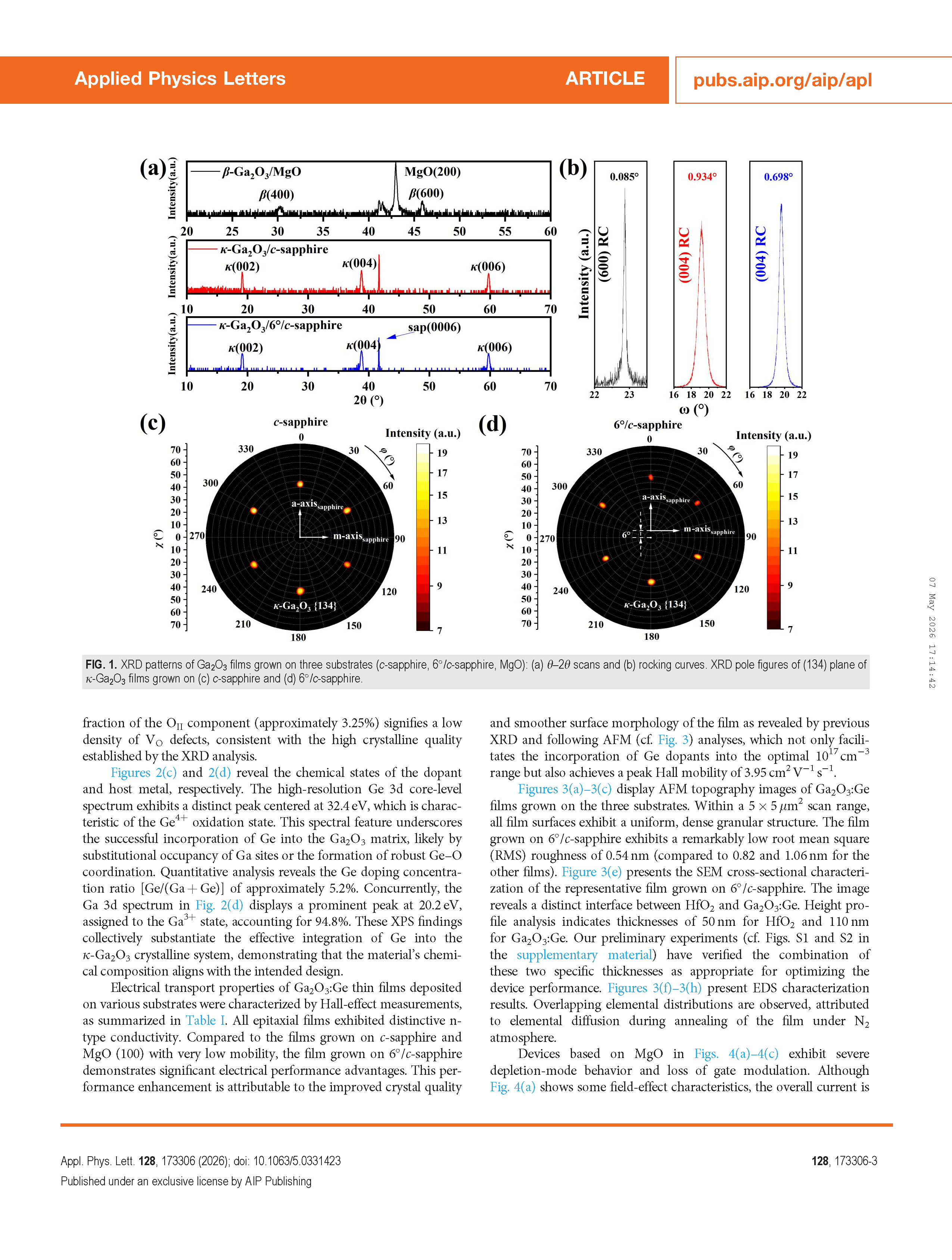
FIG. 1. XRD patterns of Ga₂O₃ films grown on three substrates (c-sapphire, 6°/c-sapphire, MgO): (a) θ–2θ scans and (b) rocking curves. XRD pole figures of (134) plane of κ-Ga₂O₃ films grown on (c) c-sapphire and (d) 6°/c-sapphire.
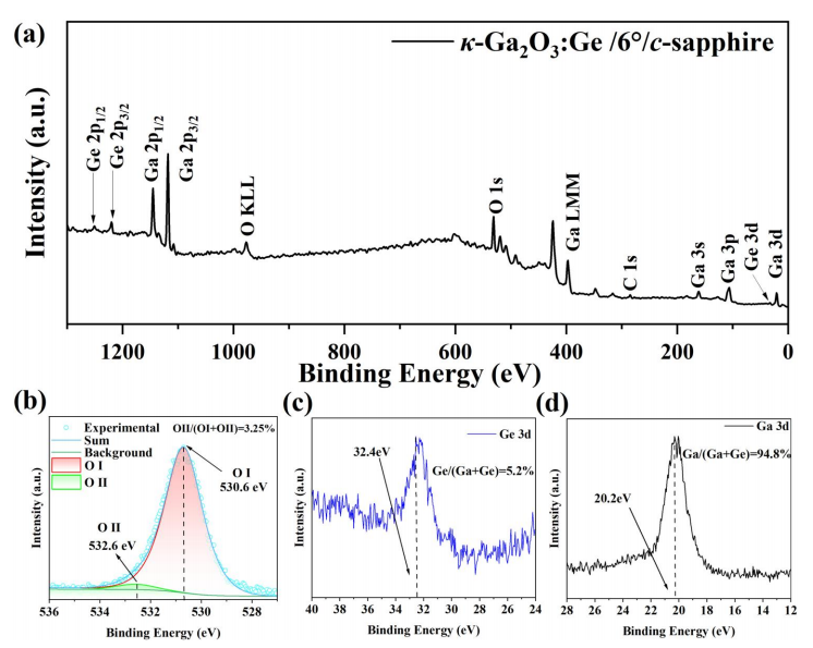
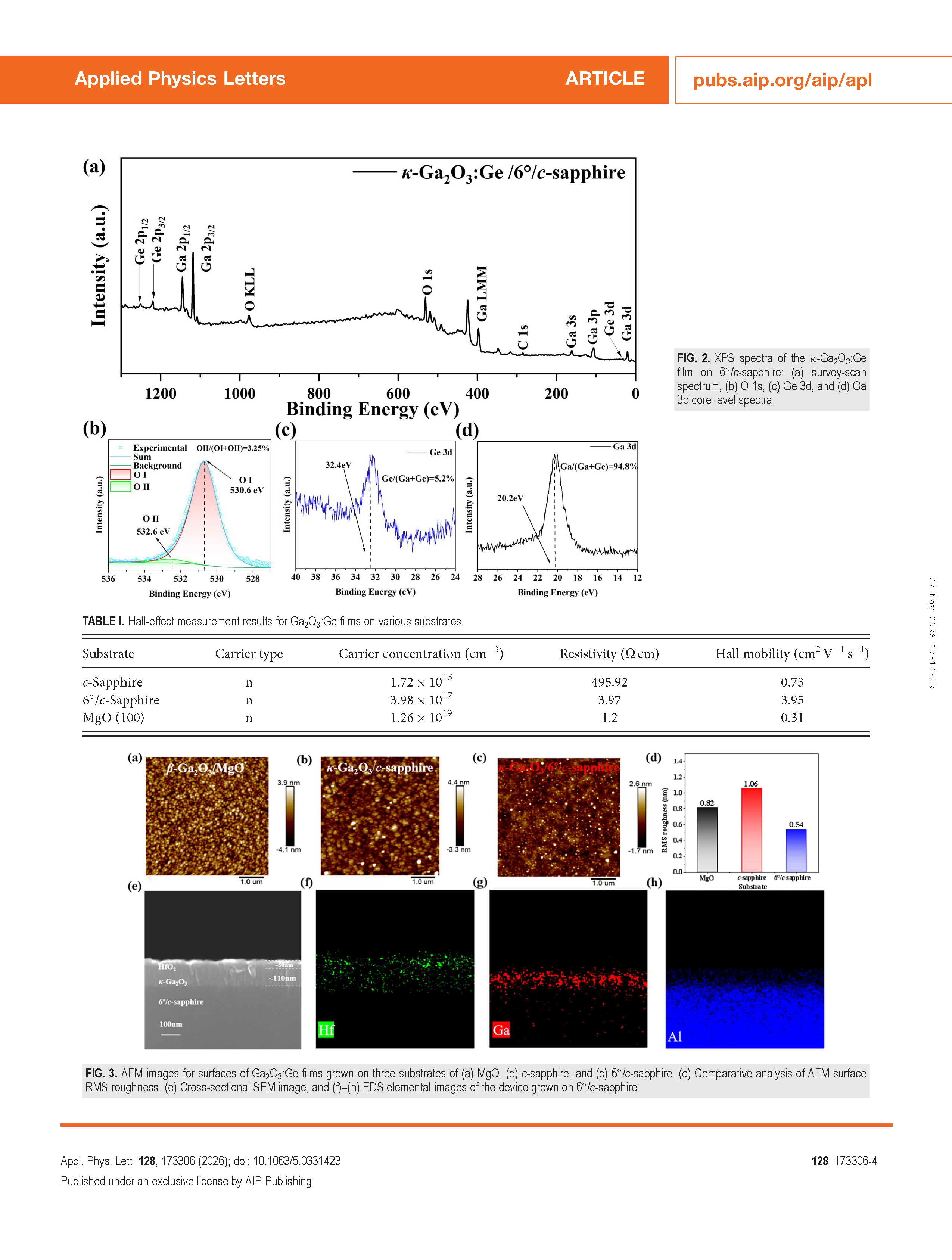
FIG. 2. XPS spectra of the κ-Ga₂O₃:Ge film on 6°/c-sapphire: (a) survey-scan spectrum, (b) O 1s, (c) Ge 3d, and (d) Ga 3d core-level spectra.
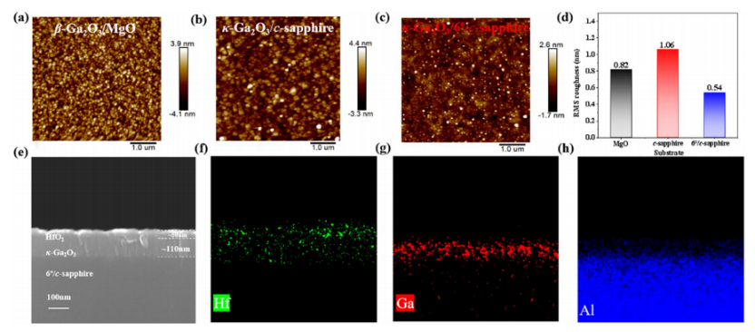
FIG. 3. AFM images for surfaces of Ga₂O₃:Ge films grown on three substrates of (a) MgO, (b) c-sapphire, and (c) 6°/c-sapphire. (d) Comparative analysis of AFM surface RMS roughness. (e) Cross-sectional SEM image, and (f)–(h) EDS elemental images of the device grown on 6°/c-sapphire.
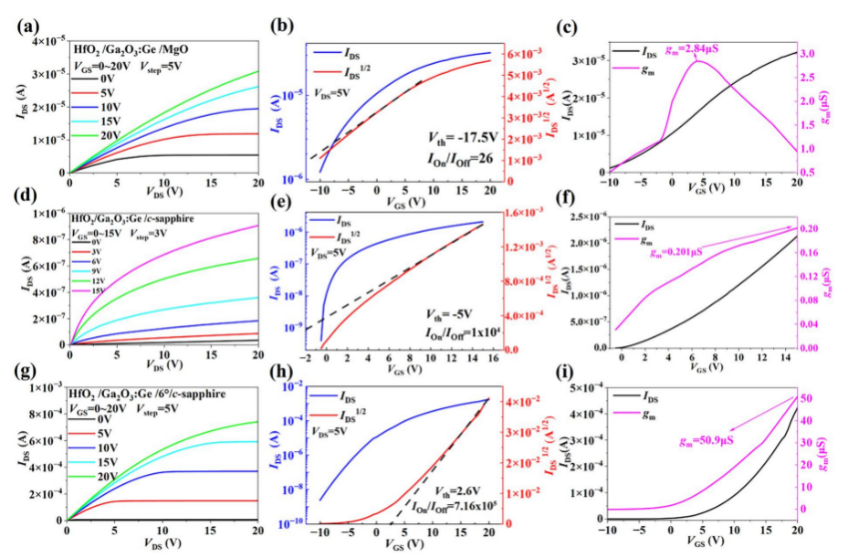
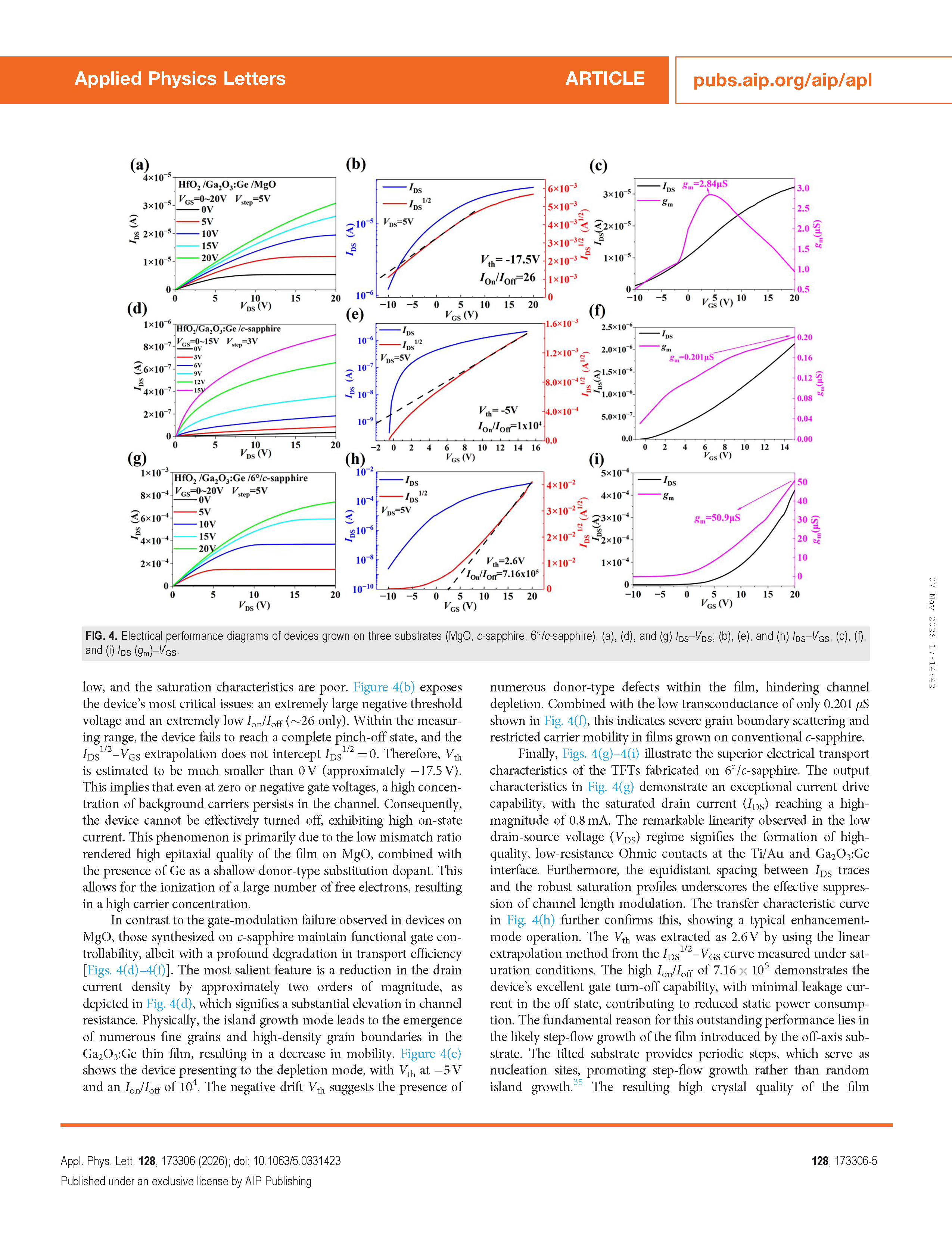
FIG. 4. Electrical performance diagrams of devices grown on three substrates (MgO, c-sapphire, 6°/c-sapphire): (a), (d), and (g) IDS–VDS; (b), (e), and (h) IDS–VGS; (c), (f), and (i) IDS (gm)–VGS.
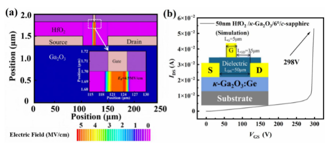
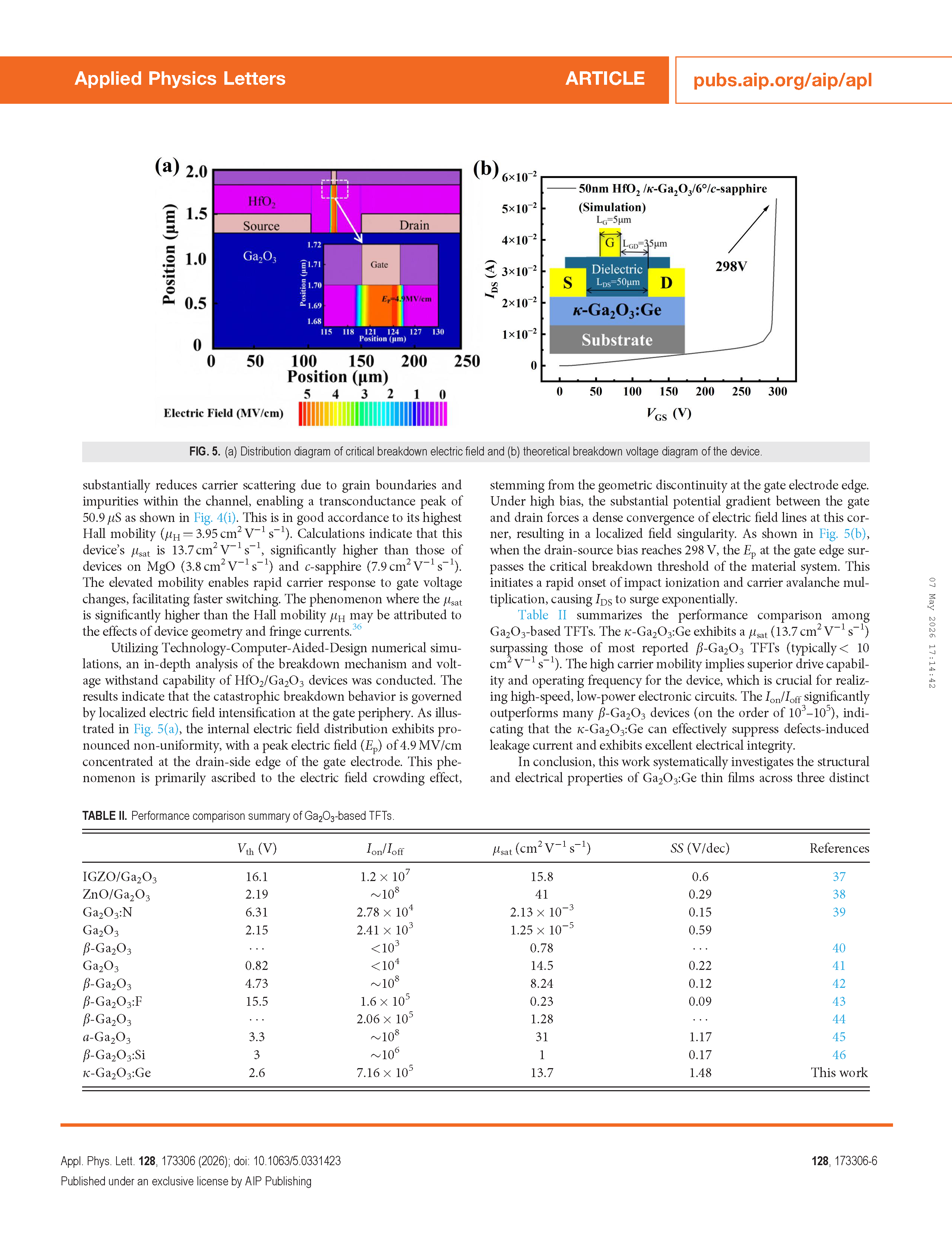
FIG. 5. (a) Distribution diagram of critical breakdown electric field and (b) theoretical breakdown voltage diagram of the device.
DOI:
doi.org/10.1063/5.0331423