Paper Sharing
【Member Papers】Study on photoelectric properties and ion implantation damage of p-type doped β-Ga₂O₃
日期:2026-05-13阅读:45
Researchers from the Xi'an University of Science and Technology have published a dissertation titled "Study on photoelectric properties and ion implantation damage of p-type doped β-Ga₂O₃" in Journal of Atomic and Molecular physics.
Background
Gallium oxide (Ga₂O₃) is an ultra-wide-bandgap semiconductor with a bandgap of approximately 4.9 eV. It possesses a high critical breakdown electric field of up to 8 MV/cm and a Baliga’s figure of merit (BFOM) of 3444, both of which significantly surpass those of wide-bandgap semiconductors such as SiC and GaN. Owing to its excellent high-voltage tolerance, high-power capability, and radiation resistance, β-Ga₂O₃ has shown great potential for applications in field-effect transistors, Schottky diodes, solar-blind ultraviolet photodetectors, and gas sensors.
Although β-Ga₂O₃ exhibits outstanding performance in the ultraviolet region, its absorption efficiency in the visible-light range is extremely low, limiting its application in broadband optoelectronic devices. Due to the presence of intrinsic oxygen vacancy defects, the material generally exhibits stable n-type conductivity. More importantly, its valence band is mainly composed of oxygen 2p orbitals, resulting in a very large hole effective mass and extremely poor hole transport properties. Consequently, achieving high-performance p-type conductivity has become one of the major bottlenecks restricting the development of Ga₂O₃-based devices.
To improve material properties, researchers commonly employ doping strategies. Among them, ion implantation is one of the mainstream industrial doping techniques because it enables precise control of dopant distribution. However, the collision process during implantation inevitably generates cascaded defects such as dislocations and vacancies, thereby causing damage to the target material.
Abstract
The p-type conductivity and optical properties of Bi and P doped β-Ga₂O₃ were investigated by first-principles calculations,combined with ion implantation simulations to study the distribution of implanted ions and the degree of damage to the target material. The calculation results indicate that Bi and P single doping introduce impurity levels,providing new pathways for electron transitions. Bi-P co-doping introduces shallow acceptor levels,among which the Bi2P2 system introduces acceptor levels at 0. 11 eV above the valence band maximum, effectively increasing the hole concentration and enhancing p-type conductivity in β-Ga₂O₃. Simultaneous Bi and P doping extends the optical absorption coefficient of β-Ga₂O₃ into the visible light region while still maintaining strong ultraviolet absorption characteristics. Further simulation of the ion implantation process showed that the ion range is approximately linearly related to the ion energy,and the P ions have a longer range and more dispersed distribution at the same ion energy. For P ions,nuclear stopping dominates at low-energy implantation, while electronic stopping dominates at high-energy implantation. For Bi ions,nuclear stopping is predominant. Furthermore,the greater the ion implantation dose,the more severe the damage to the target material.
Conclusion
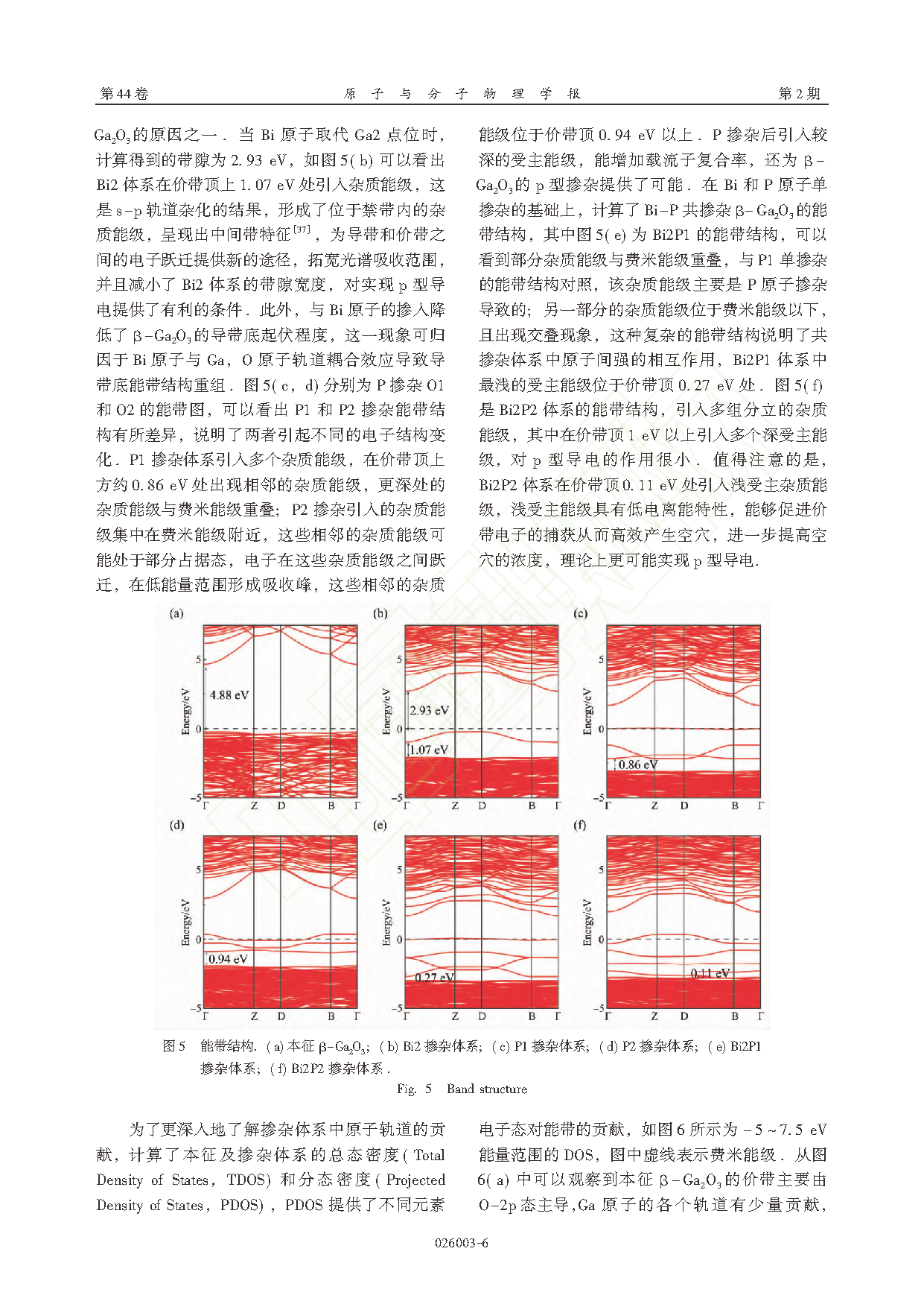
The optoelectronic properties and ion-implantation-induced damage of Bi- and P-doped β-Ga₂O₃ were investigated through a combination of density functional theory (DFT) and Monte Carlo simulations. The results show that Bi doping introduces an intermediate band and further narrows the bandgap, thereby promoting the p-type conductivity of β-Ga₂O₃ to some extent. In contrast, P doping introduces relatively deep acceptor levels, which provide new pathways for electron transitions and enhance the optical absorption capability of β-Ga₂O₃.
In the Bi–P co-doped system, shallow acceptor levels are formed. Notably, the Bi₂P₂ configuration introduces an acceptor level at 0.11 eV above the valence band maximum, which increases hole concentration and enhances p-type conductivity. Combined density of states (DOS) and charge density analyses further reveal orbital coupling and interactions between Bi and P atoms in the co-doped system. Their synergistic effect effectively improves the optoelectronic properties of β-Ga₂O₃. Optical property calculations indicate that Bi and P doping cause a redshift in the optical absorption range, extending the absorption edge into the visible-light region while maintaining strong absorption characteristics in the ultraviolet region.
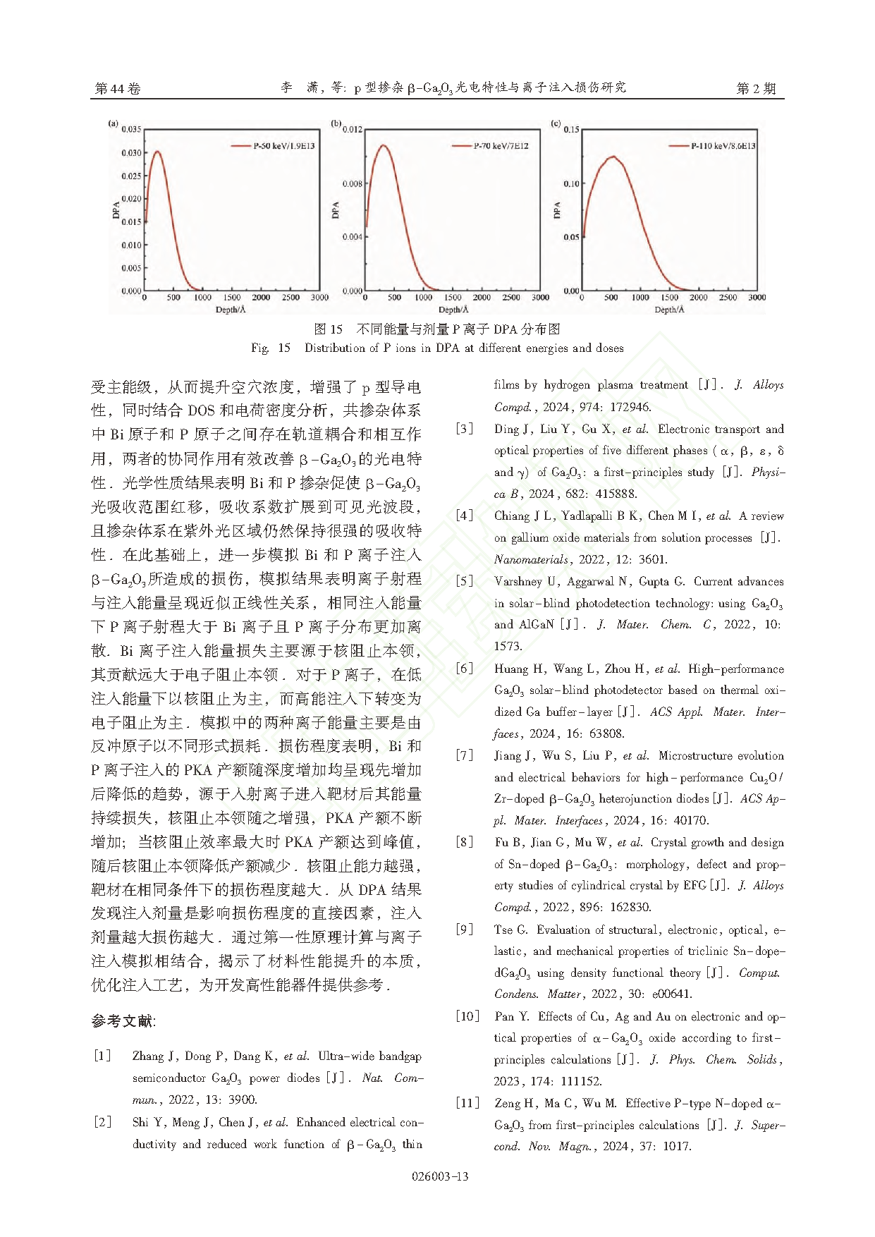
Based on these findings, the implantation damage caused by Bi and P ions in β-Ga₂O₃ was further simulated. The results demonstrate an approximately linear relationship between ion range and implantation energy. Under the same implantation energy, P ions exhibit a longer penetration range and a more dispersed distribution than Bi ions. For Bi ion implantation, energy loss is dominated by nuclear stopping power, which contributes much more significantly than electronic stopping power. In the case of P ions, nuclear stopping dominates at low implantation energies, whereas electronic stopping becomes dominant at higher energies. The energy dissipation of both implanted ions mainly occurs through recoil atoms in different forms.
Damage analysis shows that the primary knock-on atom (PKA) yield for both Bi and P implantation first increases and then decreases with depth. This behavior arises because the incident ions continuously lose energy upon entering the target material, leading to enhanced nuclear stopping and increased PKA generation. When the nuclear stopping efficiency reaches its maximum, the PKA yield peaks; afterward, the reduced nuclear stopping power causes the yield to decline. Stronger nuclear stopping capability results in more severe target damage under identical conditions. The displacement-per-atom (DPA) results further indicate that implantation dose is the direct factor affecting damage severity, with higher implantation doses causing greater damage.
By combining first-principles calculations with ion implantation simulations, this work reveals the underlying mechanisms responsible for performance enhancement, optimizes implantation processes, and provides valuable guidance for the development of high-performance β-Ga₂O₃-based devices.
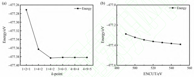
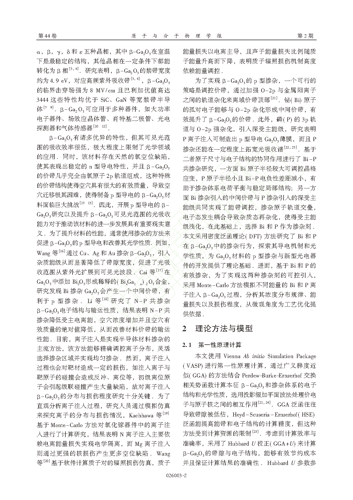
Fig. 1 Convergence tests
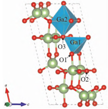
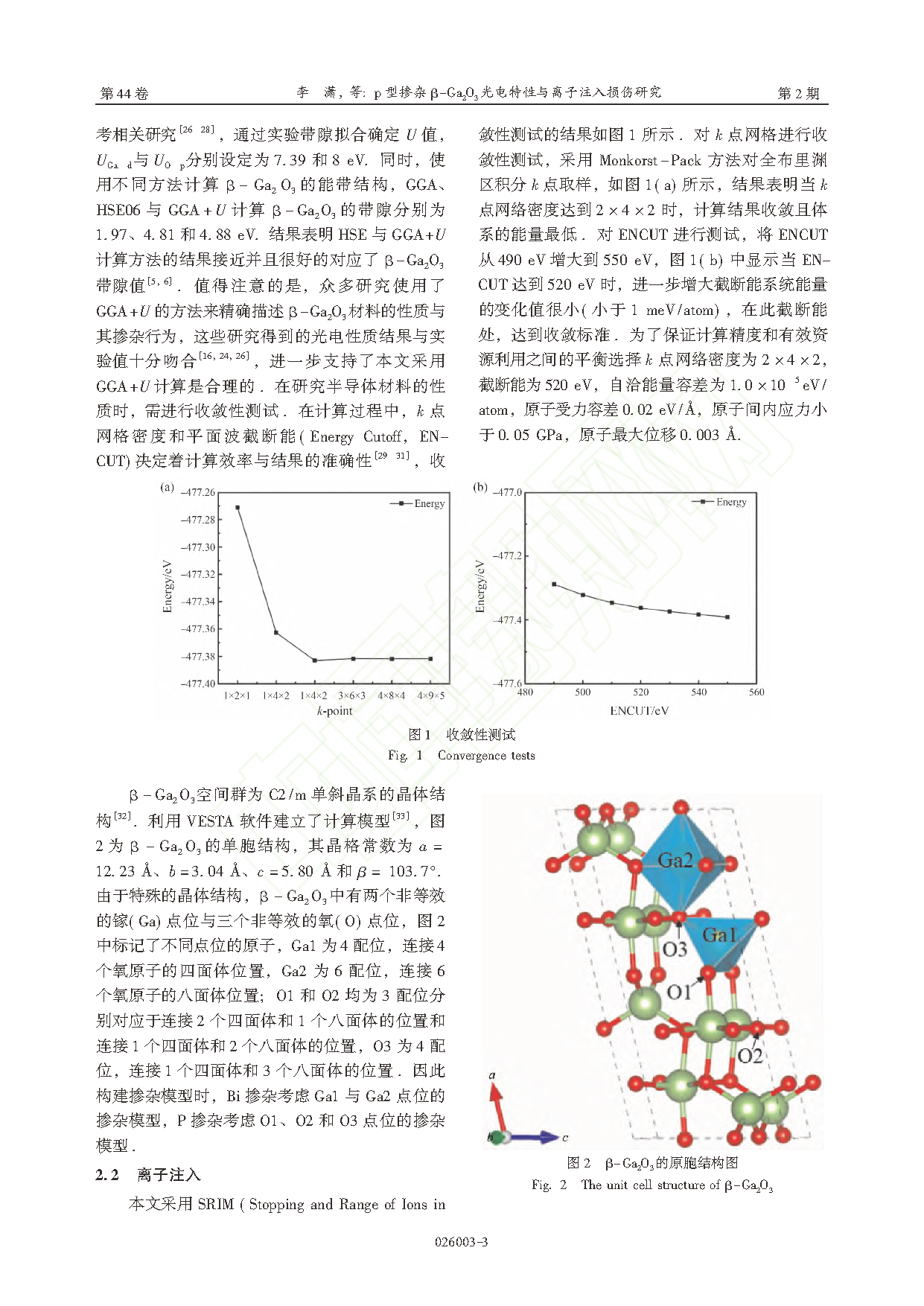
Fig. 2 The unit cell structure of β-Ga₂O₃
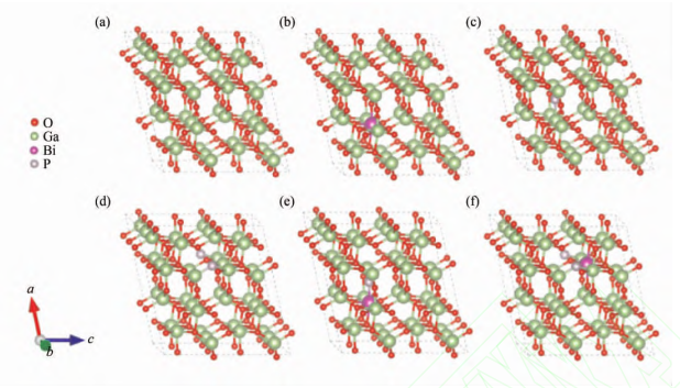
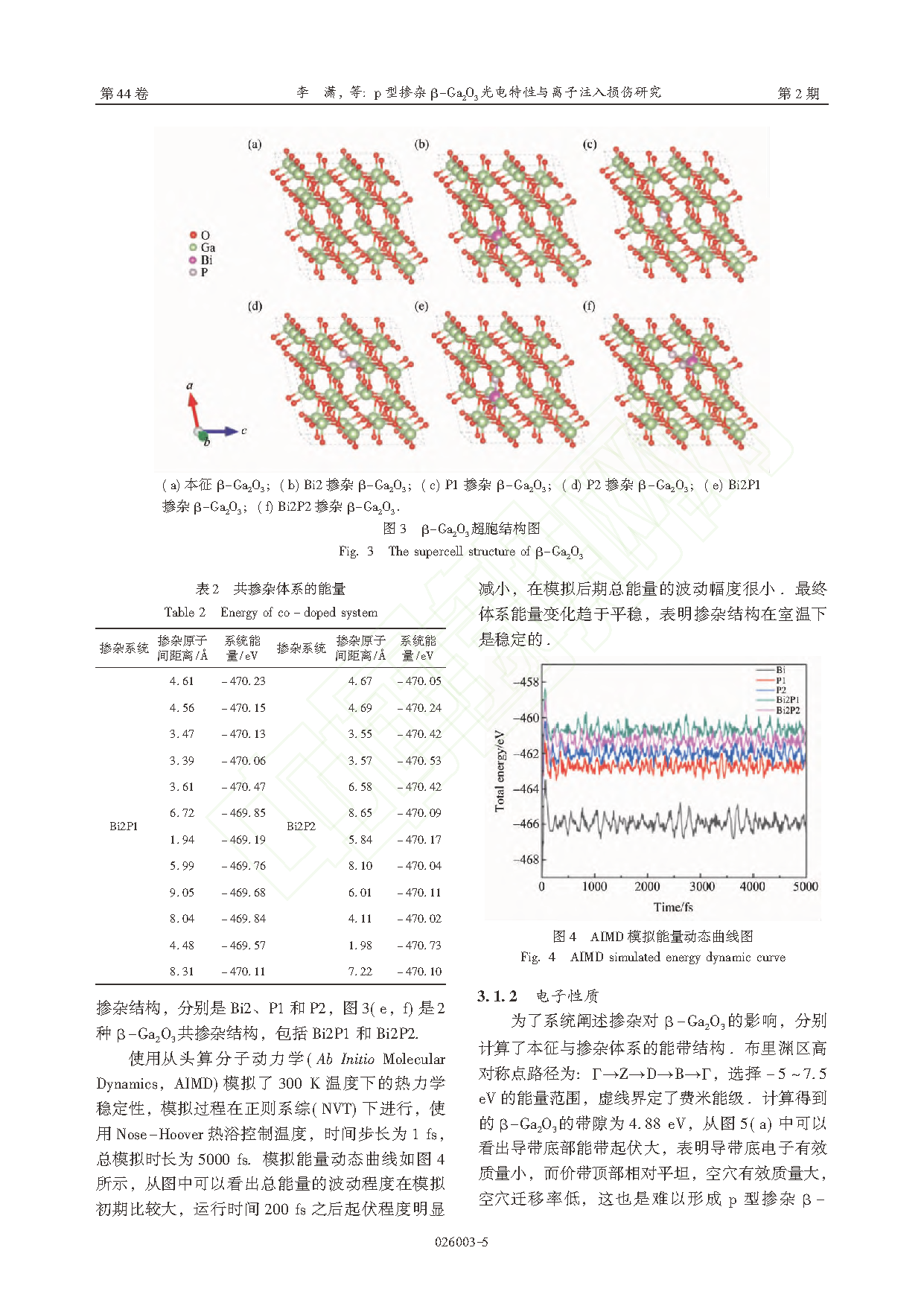
Fig. 3 The supercell structure of β-Ga₂O₃
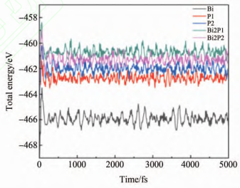
Fig. 4 AIMD simulated energy dynamic curve
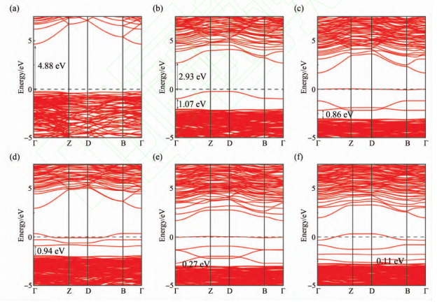
Fig. 5 Band structure
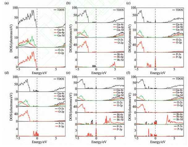
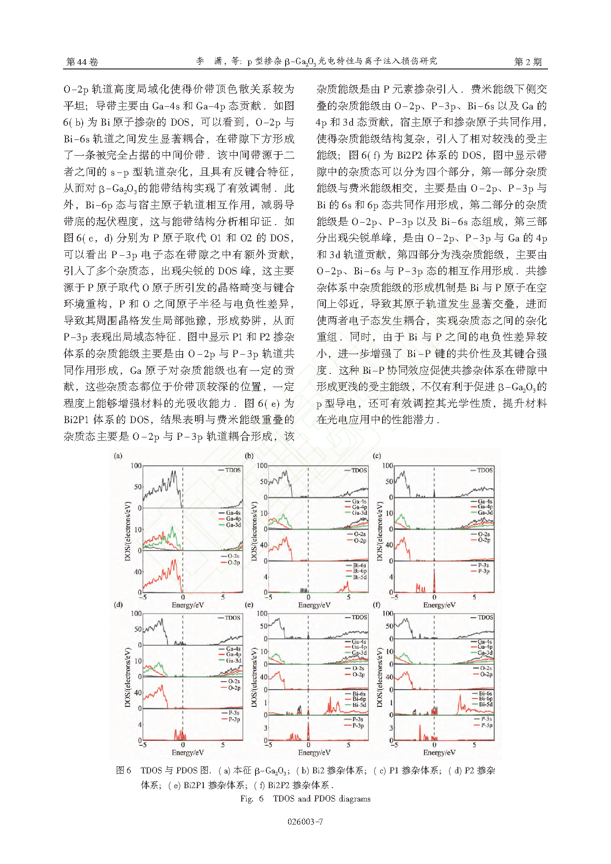
Fig. 6 TDOS and PDOS diagrams
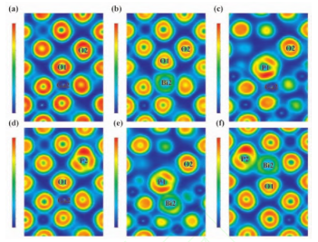
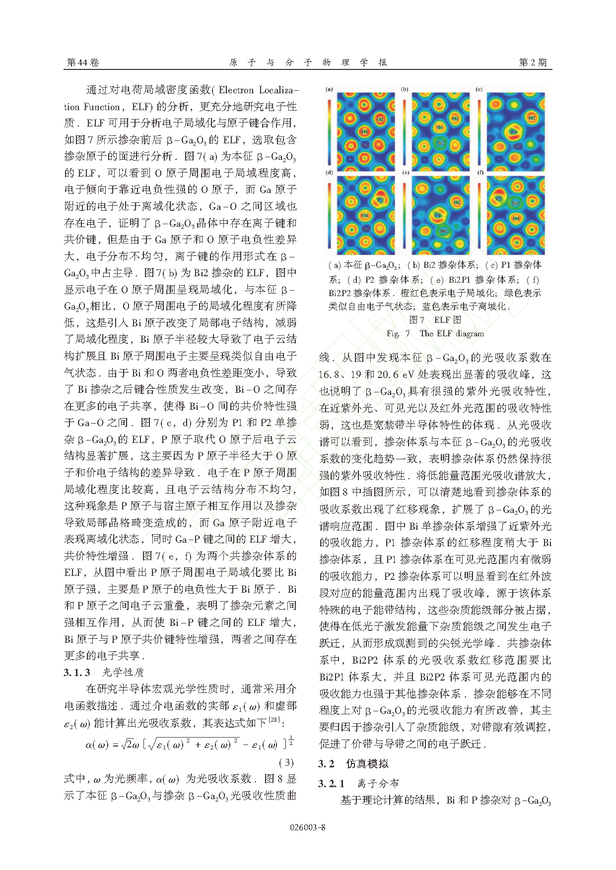
Fig. 7 The ELF diagram
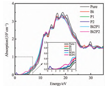
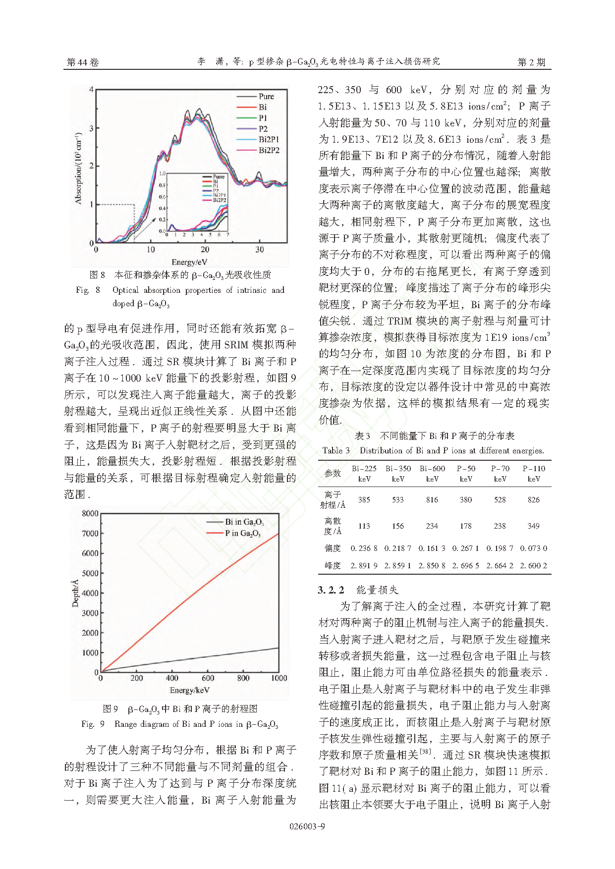
Fig. 8 Optical absorption properties of intrinsic and doped β-Ga₂O₃
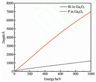
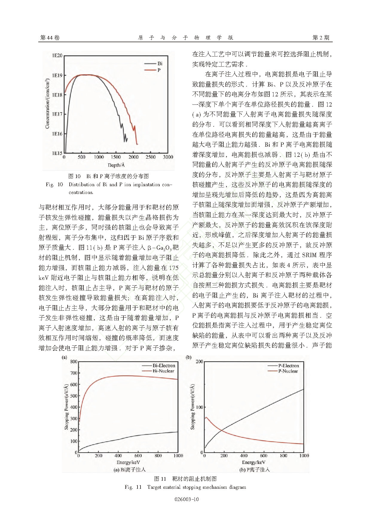
Fig. 9 Range diagram of Bi and P ions in β-Ga₂O₃
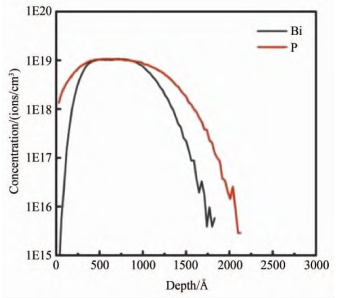
Fig. 10 Distribution of Bi and P ion implantation concentrations
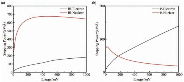
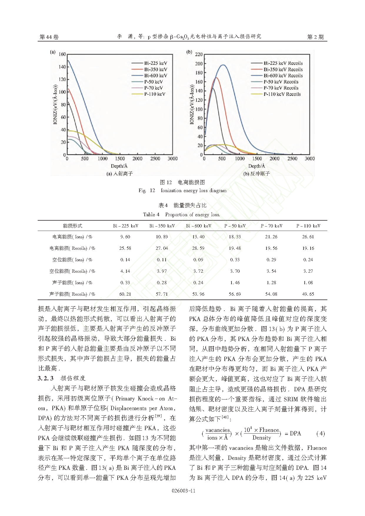
Fig. 11 Target material stopping mechanism diagram
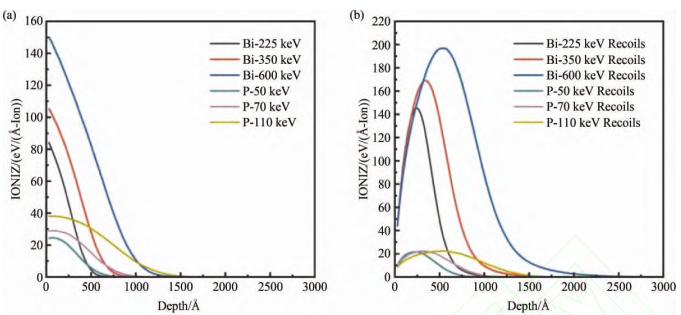
Fig. 12 Ionization energy loss diagram
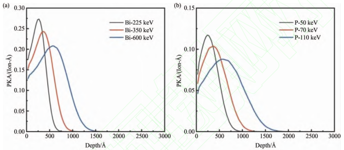
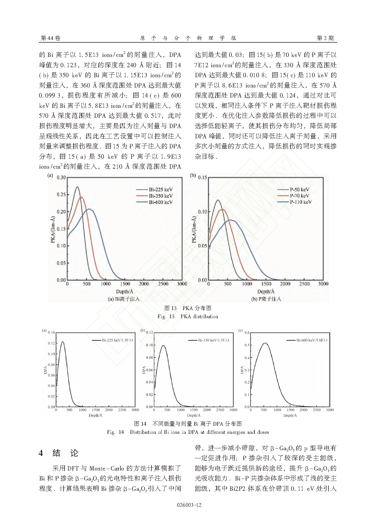
Fig. 13 PKA distribution
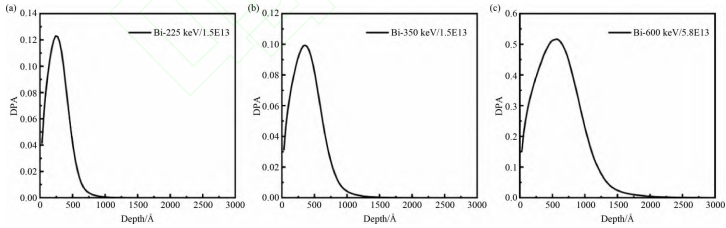
Fig. 14 Distribution of Bi ions in DPA at different energies and doses
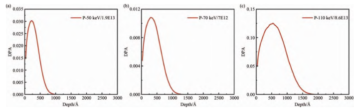
Fig. 15 Distribution of P ions in DPA at different energies and doses
Link:
https://kns.cnki.net/kcms2/article/abstract?v=8kKd7LBMH3zRDe68bQ-b7fgT0K0EBjHbXXETwDZm-8IZbbRoBl4yrXLRTxD3lLYRwFBkL0xTJKAxBlbSR78mfguaDqmFN6759Yw-gw9P44JDHRbfB2uah-fouE9NPfMb0s-PY8DojJsF3r_gSiPKObsXtA67Udcfn8bciPWT==&uniplatform=NZKPT&language=CHSlpQvvF1Bxt40zQ