Paper Sharing
【Domestic Papers】High-Performance Dual-Band Ultraviolet Photodetectors Based on Porous GaN/β-Ga₂O₃ Heterojunctions via Optimized RF Magnetron Sputtering
日期:2026-05-13阅读:41
Researchers from the University of Shanghai for Science and Technology have published a dissertation titled “High-Performance Dual-Band Ultraviolet Photodetectors Based on Porous GaN/β‑Ga₂O₃ Heterojunctions via Optimized RF Magnetron Sputtering” in Journal of Alloys and Compounds.
Background
Ultraviolet photodetectors are of great significance in environmental monitoring, communication, and military security. GaN and β‑Ga₂O₃ have become core materials for high-performance ultraviolet detection due to their suitable bandgaps. Traditional planar devices suffer from low light-harvesting efficiency and weak carrier separation. Most existing heterojunctions rely on high-temperature epitaxy or thermal oxidation, which easily introduce interfacial stress and defects, leading to high dark current and slow response. Meanwhile, low-cost and scalable strategies for bias-tunable UVC/UVA dual-band detection are still insufficient, failing to meet the requirements of low-noise, broadband-response, and integrated systems.
Abstract
Porous GaN, with a high specific surface area, enhanced light-harvesting capability, and favorable optoelectronic properties, provides an excellent platform for integrating ultravide-bandgap oxides such as β‑Ga₂O₃ toward high-performance ultraviolet (UV) photodetectors. In this study, porous GaN/β‑Ga₂O₃ heterojunction photodetectors were fabricated by room-temperature radio-frequency (RF) magnetron sputtering followed by post-annealing, and the sputtering pressure and RF power were systematically optimized to tailor the microstructure of β‑Ga₂O₃ films. An RF power of 150 W and a sputtering pressure of 0.5 Pa enable dense and uniform β‑Ga₂O₃ films with enhanced crystallinity after annealing at 900 °C. A representative heterojunction UV photodetector incorporating a 500-nm-thick β‑Ga₂O₃ layer exhibits an ultralow zero-bias dark current of 2.72 ×10⁻¹³ A and a responsivity of 70 mA·W⁻¹ under 254 nm illumination at 2 V bias, corresponding to a specific detectivity of 3.95 ×10¹¹ Jones. The device also shows fast dynamics with rise/decay times of 0.8/1.2 s. In addition, the heterojunction devices demonstrate bias-tunable dual-band UV detection, with a UVC-dominant response near 254 nm and a measurable UVA response around 365 nm that emerges above a thickness-dependent onset bias. This behavior is attributed to bias-controlled modulation of the depletion region and enhanced carrier extraction enabled by the porous GaN scaffold. These results highlight a scalable sputtering-based route to low-noise, sensitive, and spectrally tunable dual-band UV photodetectors.
Highlights
Porous GaN is used as a light-trapping scaffold to construct high-performance β‑Ga₂O₃ heterojunction photodetectors.
The sputtering pressure and RF power are optimized to obtain dense and uniform β‑Ga₂O₃ films.
The optimized device achieves an ultralow dark current of 2.72 ×10⁻¹³ A and a high detectivity of 3.95 ×10¹¹ Jones.
Bias-tunable dual-band UV detection with thickness-dependent onset voltage is realized.
The porous structure enhances light harvesting and carrier separation for improved device performance.
Conclusion
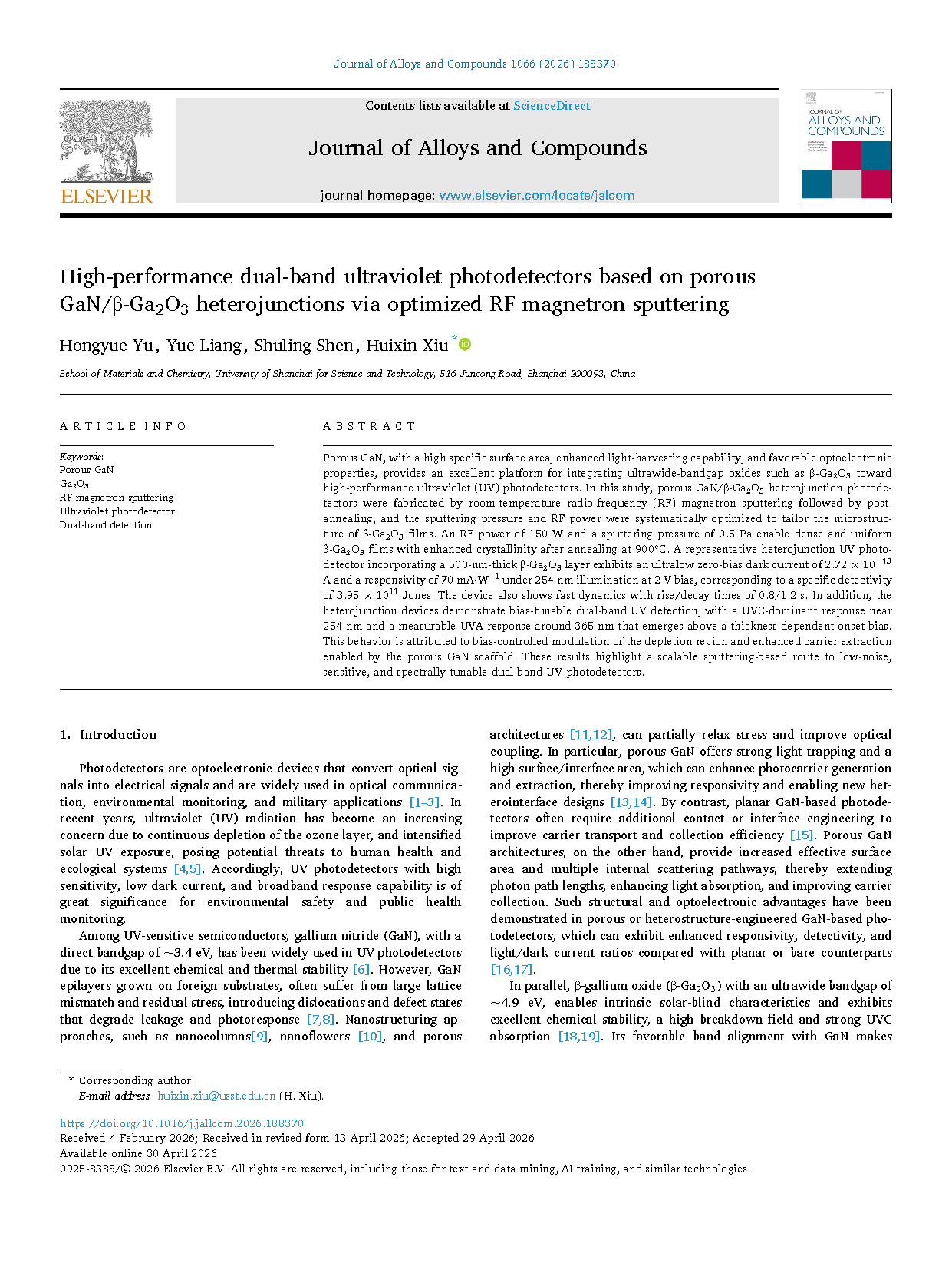
In this work, high performance dual-band UV photodetectors were realized based on porous GaN/β‑Ga₂O₃ heterojunctions fabricated via optimized RF magnetron sputtering. Porous GaN substrates with tunable porosity were prepared via photoelectrochemical etching, and a highly interconnected pore network was achieved at an etching voltage of 20 V, which enhances light trapping and enlarges the effective heterointerface area.
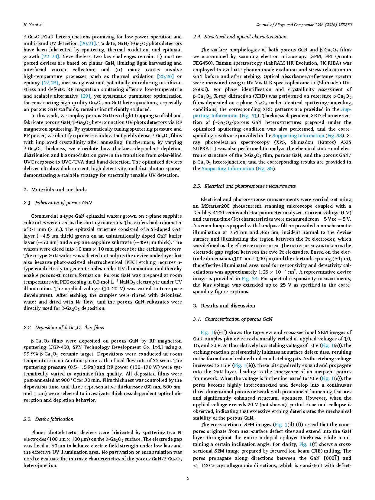
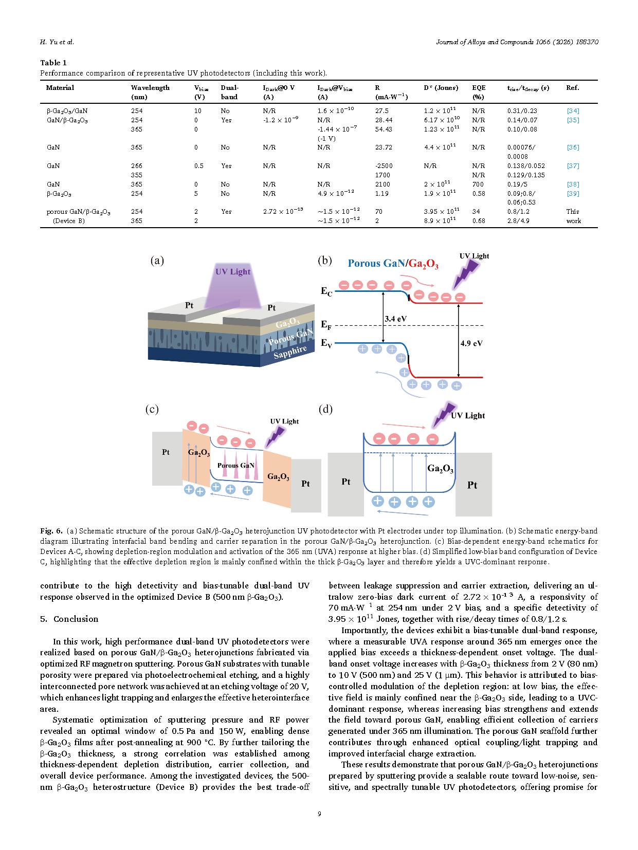
Systematic optimization of sputtering pressure and RF power revealed an optimal window of 0.5 Pa and 150 W, enabling dense β-Ga₂O₃ films after post-annealing at 900 °C. By further tailoring the β-Ga₂O₃ thickness, a strong correlation was established among thickness-dependent depletion distribution, carrier collection, and overall device performance. Among the investigated devices, the 500-nm β-Ga₂O₃ heterostructure (Device B) provides the best trade-off between leakage suppression and carrier extraction, delivering an ultralow zero-bias dark current of 2.72 × 10⁻¹³ A, a responsivity of 70 mA・W⁻¹ at 254 nm under 2 V bias, and a specific detectivity of 3.95 × 10¹¹ Jones, together with rise/decay times of 0.8/1.2 s.
Importantly, the devices exhibit a bias-tunable dual-band response, where a measurable UVA response around 365 nm emerges once the applied bias exceeds a thickness-dependent onset voltage. The dual-band onset voltage increases with β‑Ga₂O₃ thickness from 2 V (80 nm) to 10 V (500 nm) and 25 V (1 μm). This behavior is attributed to bias-controlled modulation of the depletion region: at low bias, the effective field is mainly confined near the β‑Ga₂O₃ side, leading to a UVC-dominant response, whereas increasing bias strengthens and extends the field toward porous GaN, enabling efficient collection of carriers generated under 365 nm illumination. The porous GaN scaffold further contributes through enhanced optical coupling/light trapping and improved interfacial charge extraction.
These results demonstrate that porous GaN/β‑Ga₂O₃ heterojunctions prepared by sputtering provide a scalable route toward low-noise, sensitive, and spectrally tunable UV photodetectors, offering promise for environmental monitoring, flame sensing, and UV optical communication.
Project Support
This work was supported by the National Key R&D Program of China (Grant No. 2022YFE0107400), Shanghai Pujiang Program (22PJD046), the National Natural Science Foundation of China (Grant No. 11704251) and China Scholarship Council (No. 202308310199).
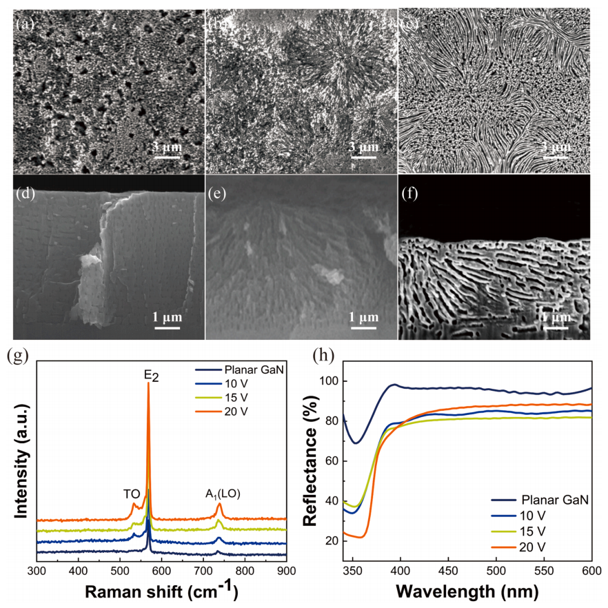
Fig. 1. Top-view and cross-sectional SEM images of GaN samples photoelectrochemically etched at different voltages: (a)-(c) surface morphologies at 10, 15, and 20 V; (d)-(f) corresponding cross-sectional morphologies at 10, 15, and 20 V. (g) Raman spectra of porous GaN etched at different voltages. (h) Reflectance spectra of porous GaN etched at different voltages.
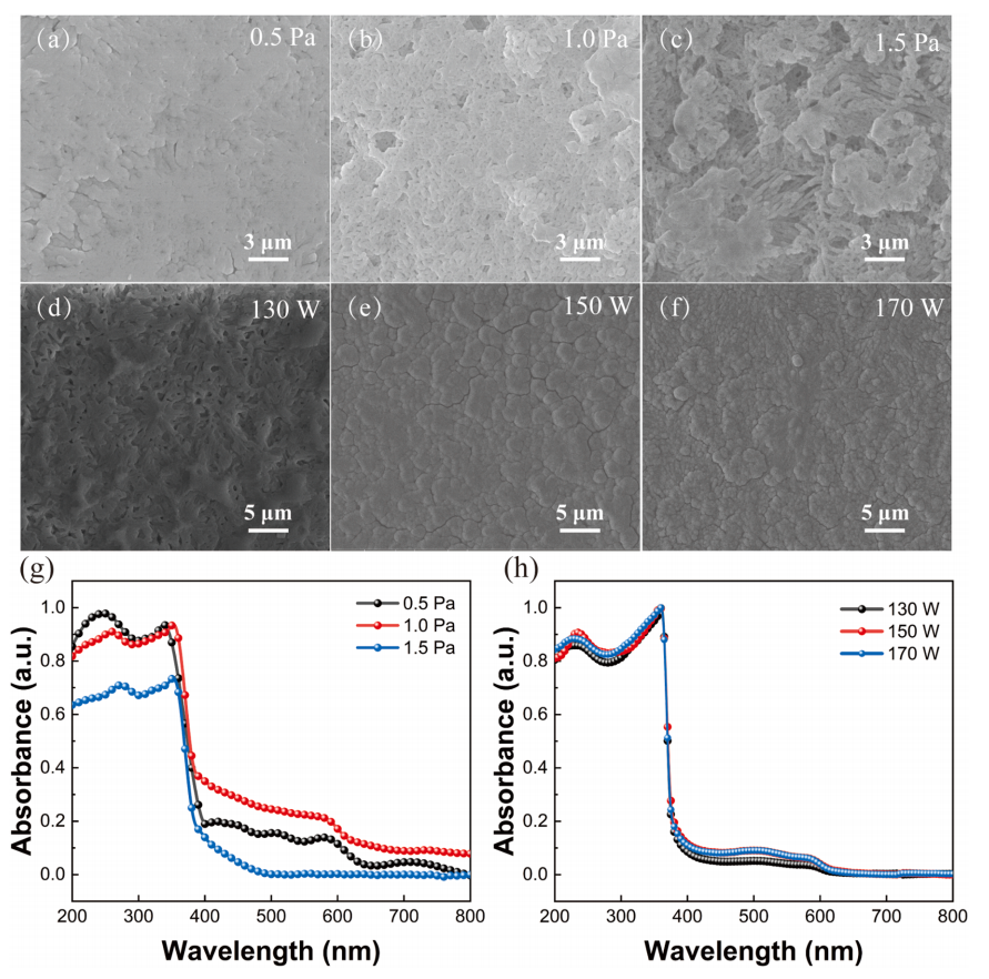
Fig. 2. Top-view SEM images of β‑Ga₂O₃ deposited under different sputtering pressures and RF powers: (a) 0.5 Pa, 150 W; (b) 1.0 Pa, 150 W; (c) 1.5 Pa, 150 W; (d) 0.5 Pa, 130 W; (e) 0.5 Pa, 150 W; (f) 0.5 Pa, 170 W. (g) Absorbance of porous GaN/β‑Ga₂O₃ heterojunctions prepared under different sputtering pressures. (h) Absorbance of porous GaN/β‑Ga₂O₃ heterojunctions prepared under different RF powers.
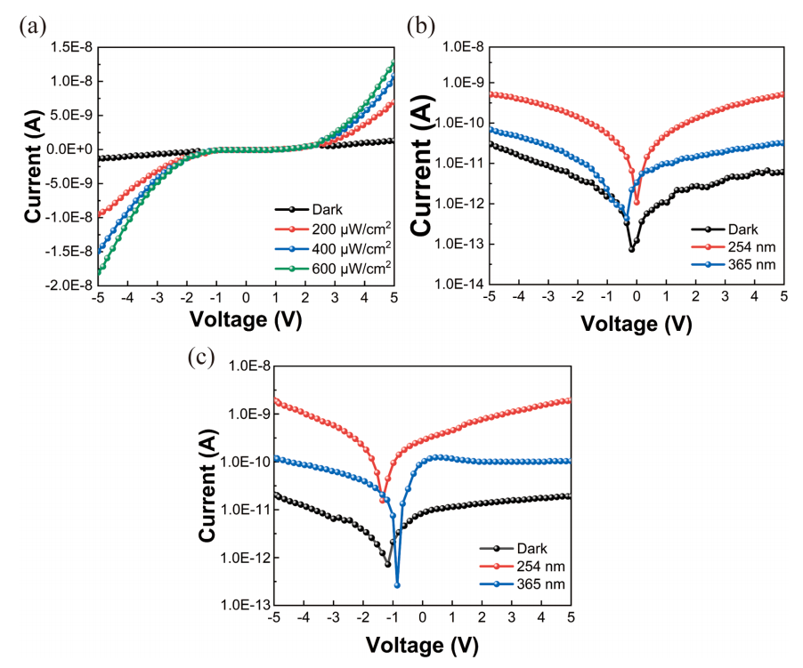
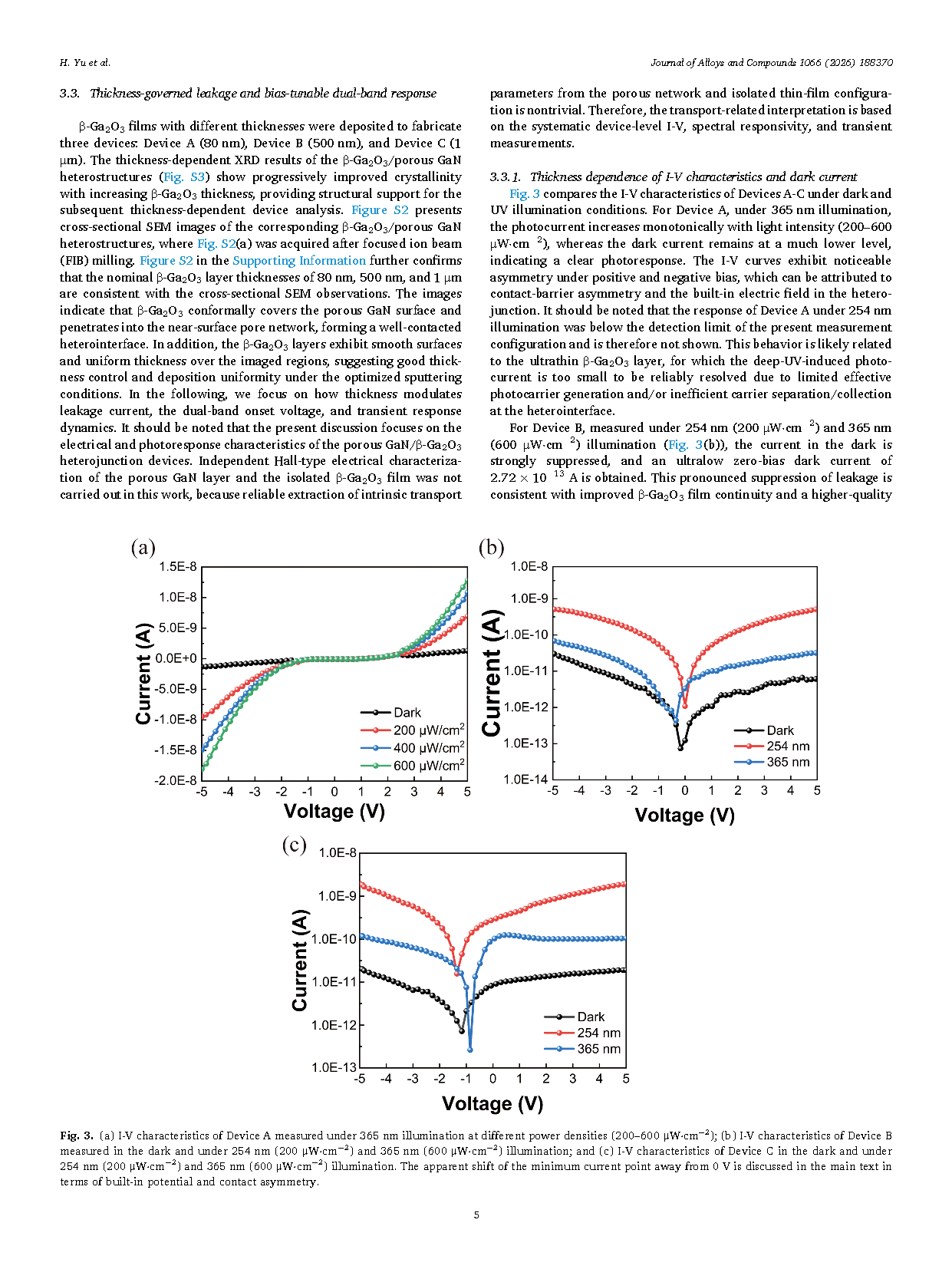
Fig. 3. (a) I-V characteristics of Device A measured under 365 nm illumination at different power densities (200–600 μW・cm⁻²); (b) I-V characteristics of Device B measured in the dark and under 254 nm (200 μW・cm⁻²) and 365 nm (600 μW・cm⁻²) illumination; and (c) I-V characteristics of Device C in the dark and under 254 nm (200 μW・cm⁻²) and 365 nm (600 μW・cm⁻²) illumination.
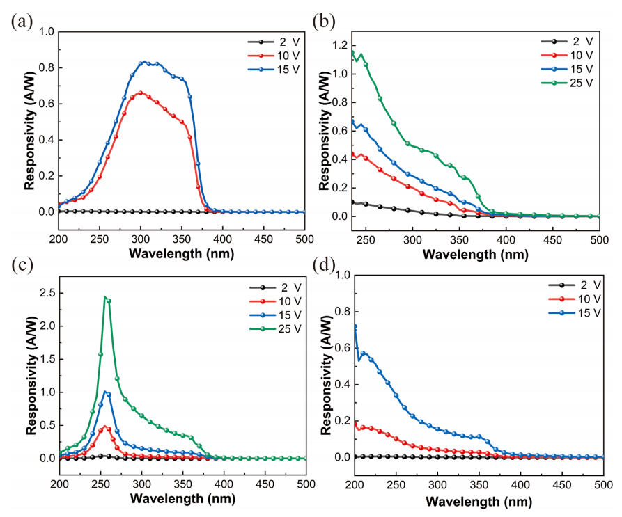
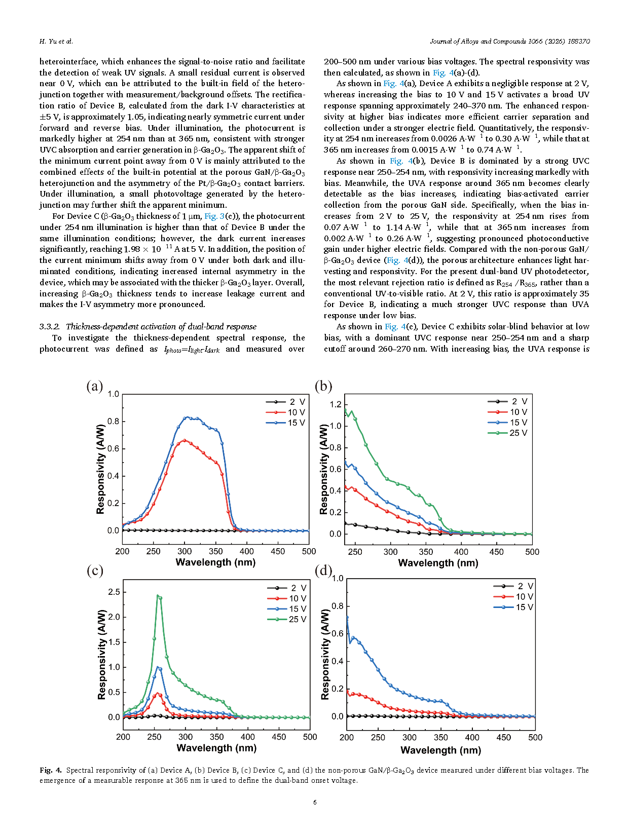
Fig. 4. Spectral responsivity of (a) Device A, (b) Device B, (c) Device C, and (d) the non-porous GaN/β‑Ga₂O₃ device measured under different bias voltages. The emergence of a measurable response at 365 nm is used to define the dual-band onset voltage.
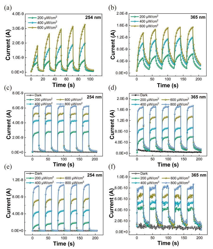
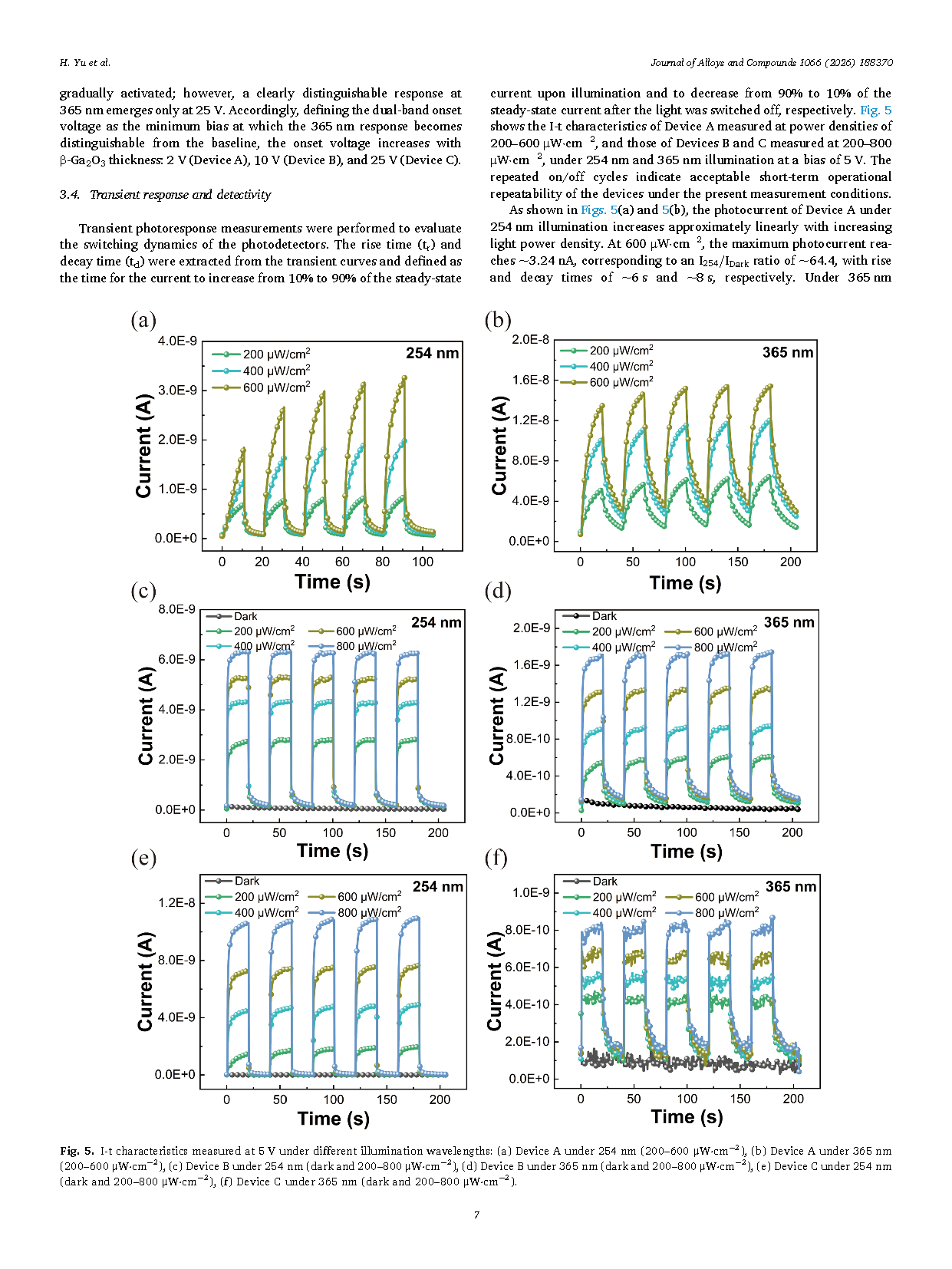
Fig. 5. I-t characteristics measured at 5 V under different illumination wavelengths: (a) Device A under 254 nm (200–600 μW・cm⁻²), (b) Device A under 365 nm (200–600 μW・cm⁻²), (c) Device B under 254 nm (dark and 200–800 μW・cm⁻²), (d) Device B under 365 nm (dark and 200–800 μW・cm⁻²), (e) Device C under 254 nm (dark and 200–800 μW・cm⁻²), (f) Device C under 365 nm (dark and 200–800 μW・cm⁻²).
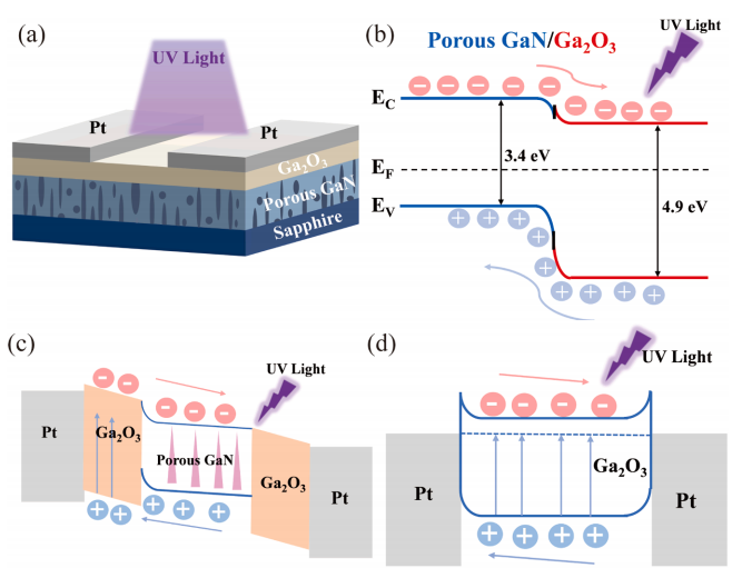
Fig. 6. (a) Schematic structure of the porous GaN/β‑Ga₂O₃ heterojunction UV photodetector with Pt electrodes under top illumination. (b) Schematic energy-band diagram illustrating interfacial band bending and carrier separation in the porous GaN/β‑Ga₂O₃ heterojunction. (c) Bias-dependent energy-band schematics for Devices A-C, showing depletion-region modulation and activation of the 365 nm (UVA) response at higher bias. (d) Simplified low-bias band configuration of Device C, highlighting that the effective depletion region is mainly confined within the thick β‑Ga₂O₃ layer and therefore yields a UVC-dominant response.
DOI:
doi.org/10.1016/j.jallcom.2026.188370