Paper Sharing
【Domestic Papers】Lattice-Rotating SrTiO₃ Buffer Enables Self-Powered DUV/NIR Dual-Band Ga₂O₃/GaAs Photodetectors with Wavelength-Polarity Locking for Optical Encryption
日期:2026-05-11阅读:51
Researchers from the Beijing University of Posts and Telecommunications have published a dissertation titled "Lattice-Rotating SrTiO₃ Buffer Enables Self-Powered DUV/NIR Dual-Band Ga₂O₃/GaAs Photodetectors with Wavelength-Polarity Locking for Optical Encryption" in Laser & Photonics Reviews.
Background
With the rapid development of the Internet of Things (IoT), secure tactical communications, and multimodal sensing technologies, there is an increasing demand for photodetectors capable of simultaneously detecting different spectral bands, such as deep ultraviolet (DUV, 200–280 nm) and near-infrared (NIR, 700–1100 nm). Due to the strong absorption of stratospheric ozone, background noise at the Earth’s surface in the DUV region is extremely low. In addition, atmospheric attenuation limits transmission distance, giving DUV signals an inherent anti-eavesdropping capability and making them highly suitable for short-range non-line-of-sight (NLOS) communication. Meanwhile, NIR technologies offer mature device platforms, high data transmission rates, and excellent penetration capability.
Heterogeneous integration of wide-bandgap oxides such as gallium oxide (Ga₂O₃) with mature III–V semiconductors like GaAs represents an effective route toward next-generation multimodal optoelectronic devices. However, the large lattice mismatch between these two material systems poses a major challenge. Developing effective interface engineering strategies to eliminate interfacial stress and achieve high-quality epitaxial growth remains a key bottleneck in the field. Furthermore, to meet the demands of edge computing and portable electronics, the development of self-powered optoelectronic devices with hardware-level security features has become an important research direction.
Abstract
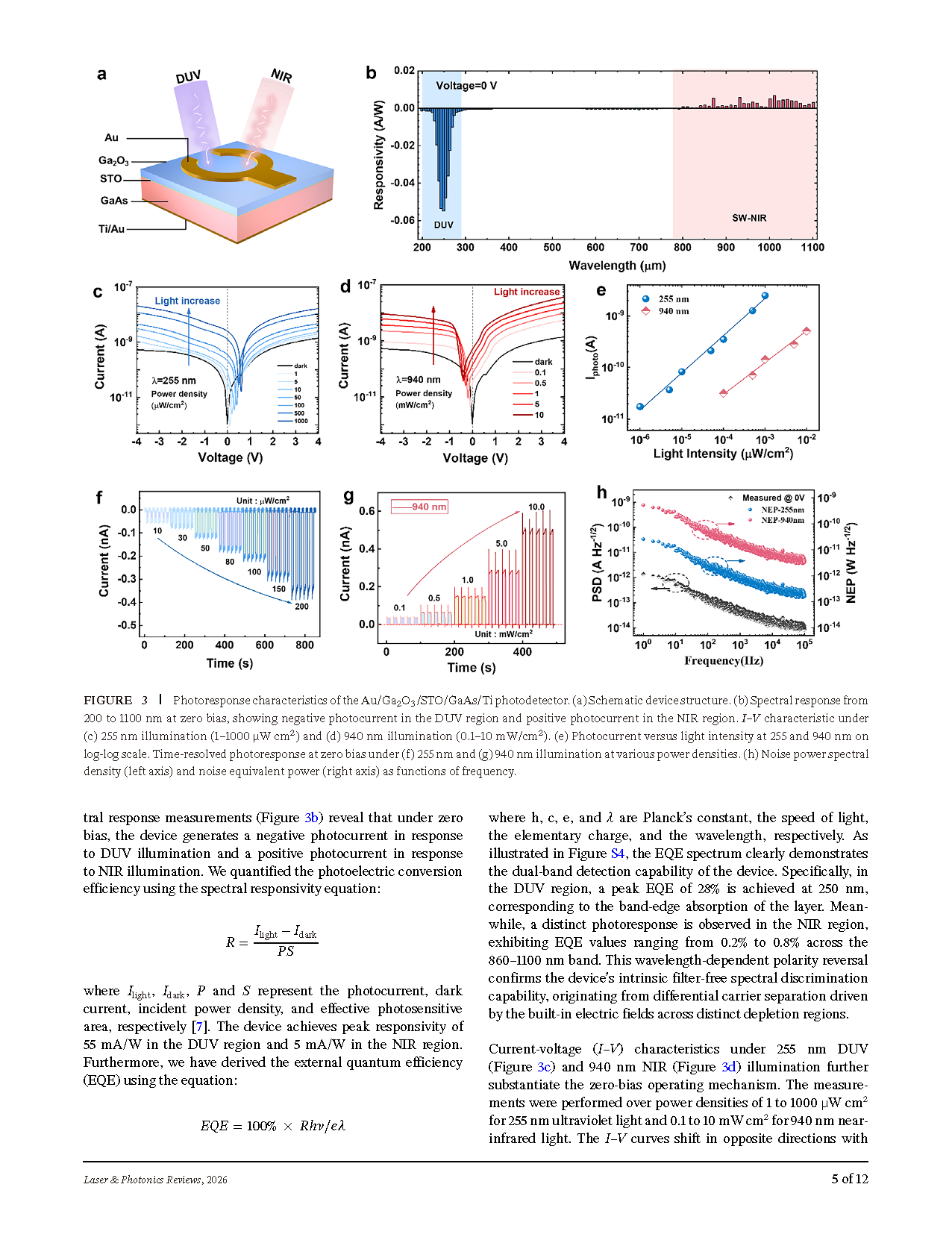
Heterogeneous integration of wide-bandgap oxides with mature III-V semiconductors off promising opportunities for next-generation multimodal optoelectronics, but remains challenging due to the substantial lattice mismatch between these dissimilar material systems. Here, it is overcome this limitation by introducing a SrTiO3 (STO) buffer layer that accommodates interfacial strain through a lattice-rotation mechanism, enabling high-quality epitaxial growth of Ga2O3 on GaAs substrates. Leveraging this heterostructure, a vertical Au/Ga2O3/STO/GaAs/Ti photodetector that achieves self-powered, polarity-switchable dual-band detection is fabricated. The device exhibits a responsivity of 55 mA/W with negative polarity photocurrent for 255 nm solar-blind ultraviolet light and 5 mA/W with positive photoconductor for 940 nm near-infrared light, accompanied by rapid response times of 1.56 and 1.04 ms, respectively. It is attributed this bidirectional photoresponse to opposing built-in electric fields established at the top Au/Ga2O3 Schottky junction and the bottom Ga2O3/STO/GaAs heterojunction, which selectively drive photogenerated carriers in opposite directions depending on the incident wavelength. Exploiting this wavelength-polarity locking effect, filter-free wavelength-division multiplexing (WDM) communication and hardware-level optical image encryption is demonstrated. This work provides an effective interface engineering strategy for large-mismatch heteroepitaxy and opens a pathway toward secure, zero-power optoelectronic systems.
Highlight
By introducing an STO buffer layer and utilizing a lattice-rotation mechanism to regulate interfacial stress, the large lattice mismatch between Ga₂O₃ and GaAs was successfully overcome, enabling high-quality epitaxial integration.
A vertical Au/Ga₂O₃/STO/GaAs/Ti device structure was constructed, achieving sensitive responses to both 255 nm ultraviolet light and 940 nm near-infrared light under zero-bias conditions.
Taking advantage of the polarity-switching characteristics, the research team successfully demonstrated filter-free wavelength division multiplexing (WDM) communication as well as highly secure hardware-level optical image encryption technology.
Conclusions
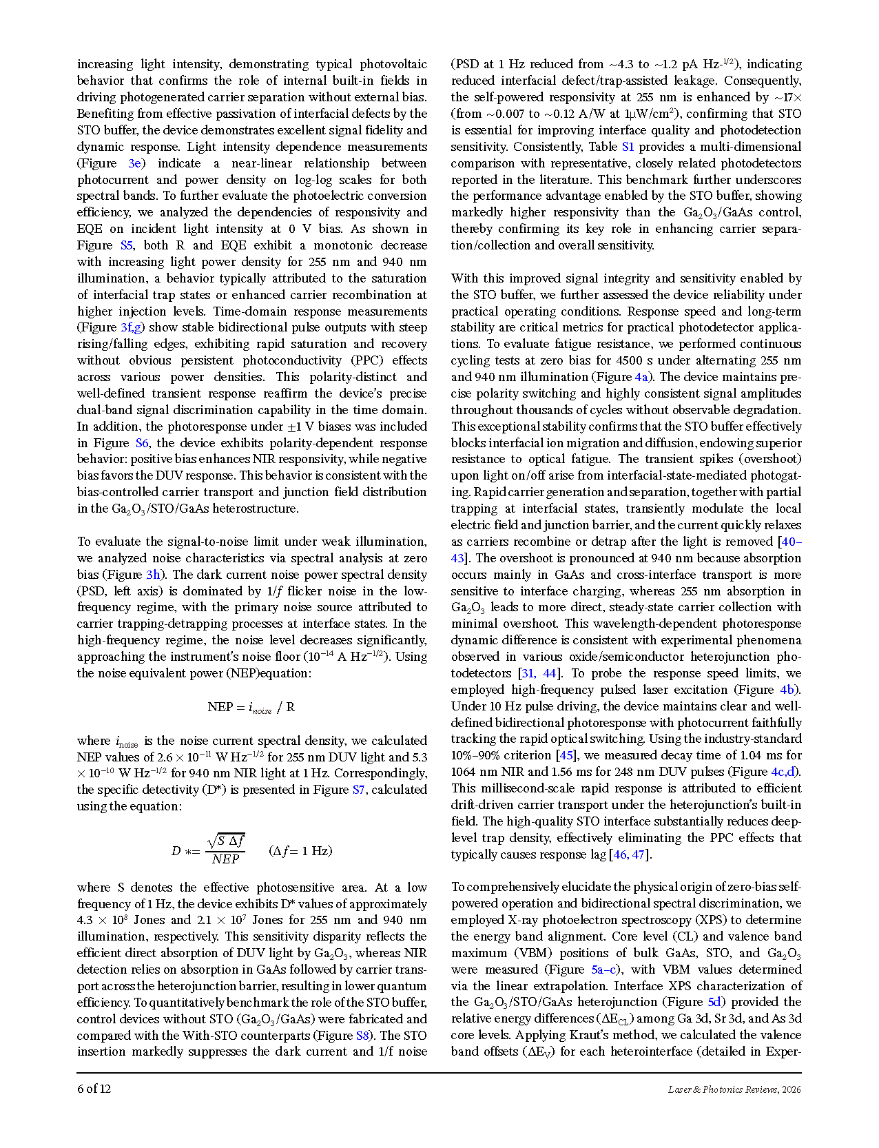
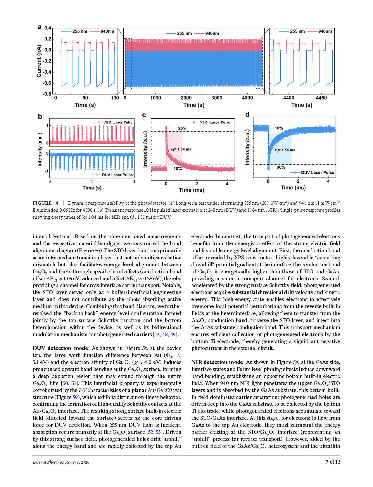
In summary, we have overcome the substantial lattice mismatch between the β-Ga₂O₃ and GaAs substrates by introducing a STO buffer layer that accommodates interfacial strain through a 45° lattice-rotation mechanism. This strategy reduces the anisotropic mismatch from 6.32% to ∼4% in both orthogonal directions, enabling high-quality heteroepitaxial growth with RMS surface roughness reduced by over 50%. Leveraging this platform, we demonstrated a vertical Au/Ga₂O₃/STO/GaAs/Ti photodetector that achieves simultaneous DUV (255 nm) and NIR (940 nm) detection with zero crosstalk. The device exhibits responsivities of 55 mA/W (DUV) and 5 mA/W (NIR), rapid response times (1.56 ms for DUV, 1.04 ms for NIR), and ultra-low noise equivalent power (NEP = 2.6 × 10⁻¹¹ W Hz−1/2 for DUV). This bidirectional response originates from the back-to-back built-in electric fields, which selectively drive photogenerated carrier in opposite directions depending on incident wavelength. This work not only establishes an effective interface engineering strategy for large-mismatch heteroepitaxy but also paves the way for next-generation compact, secure, and low-power dual-band optoelectronic systems.
By realizing crosstalk-free DUV/NIR simultaneous detection in a compact, self-powered device, we overcome the trade-off between integration density and detection fidelity that plagues conventional dual-band systems. The self-powered operation, enabled by the built-in electric fields, aligns with the low-power requirements of IoT and portable sensing devices. Furthermore, the wavelength-polarity locking effect provides a hardware-level solution for WDM communication and optical encryption — critical for applications where data security and real-time processing are paramount. Unlike software-based encryption, hardware-level spectral discrimination is resistant to hacking and reduces latency, making it suitable for high-security tactical communication and classified data transfer.
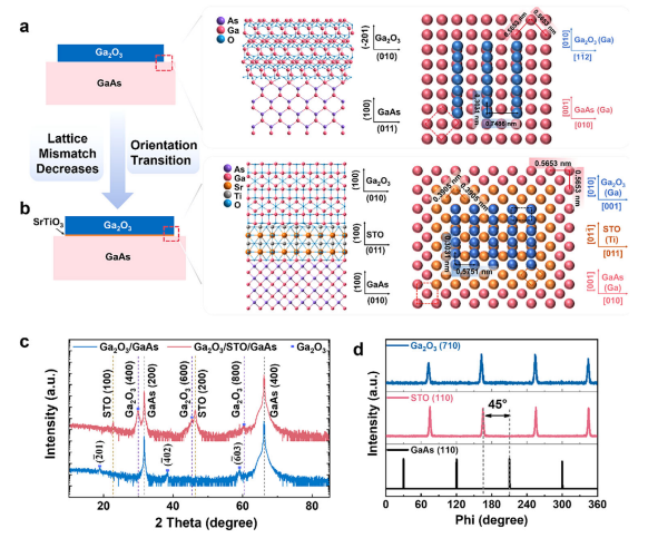
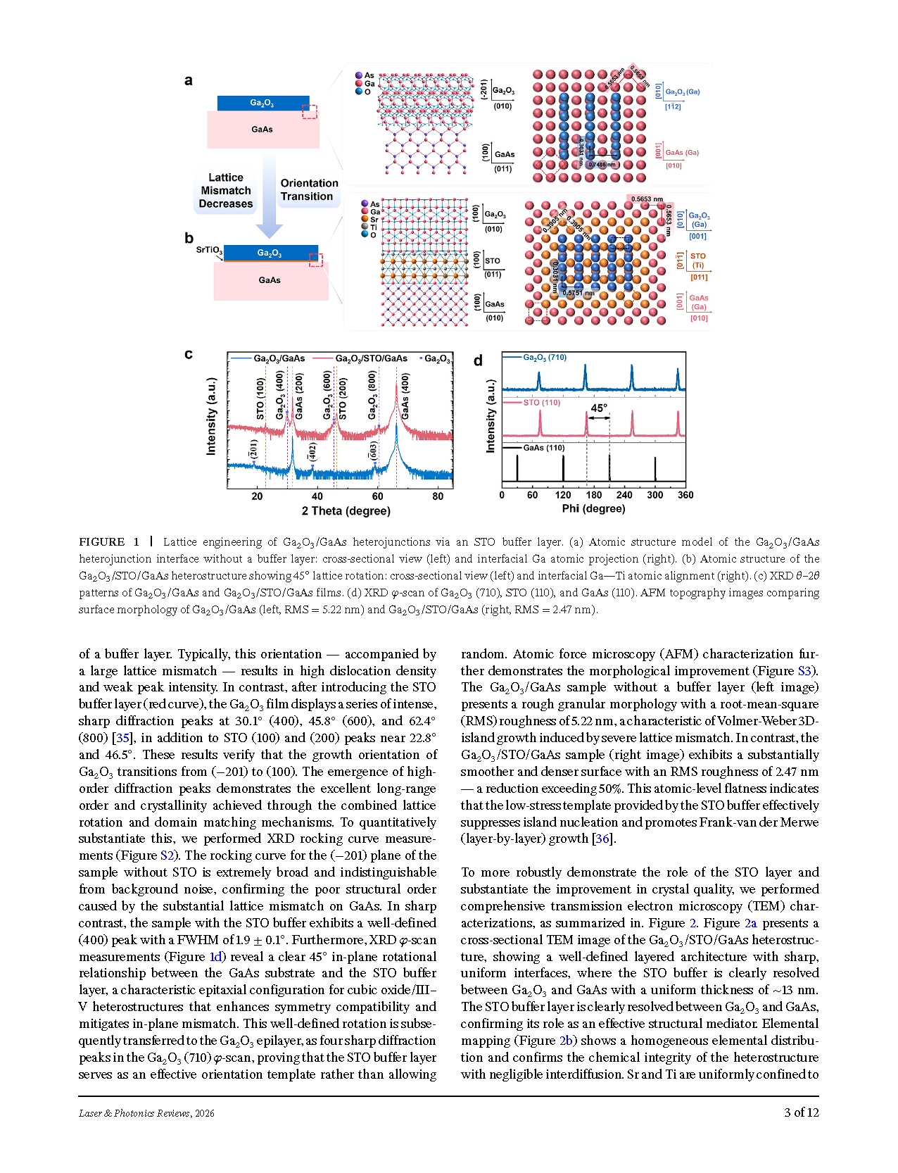
FIGURE 1. Lattice engineering of Ga₂O₃/GaAs heterojunctions via an STO buffer layer. (a) Atomic structure model of the Ga₂O₃/GaAs heterojunction interface without a buffer layer: cross-sectional view (left) and interfacial Ga atomic projection (right). (b) Atomic structure of the Ga₂O₃/STO/GaAs heterostructure showing 45◦ lattice rotation: cross-sectional view (left) and interfacial Ga—Ti atomic alignment (right). (c) XRD θ–2θ patterns of Ga₂O₃/GaAs and Ga₂O₃/STO/GaAs films. (d) XRD φ-scan of Ga₂O₃ (710), STO (110), and GaAs (110). AFM topography images comparing surface morphology of Ga₂O₃/GaAs (left, RMS = 5.22 nm) and Ga₂O₃/STO/GaAs (right, RMS = 2.47 nm).
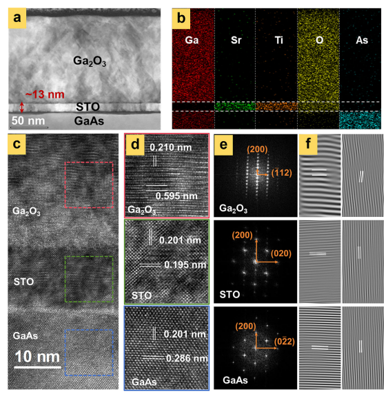
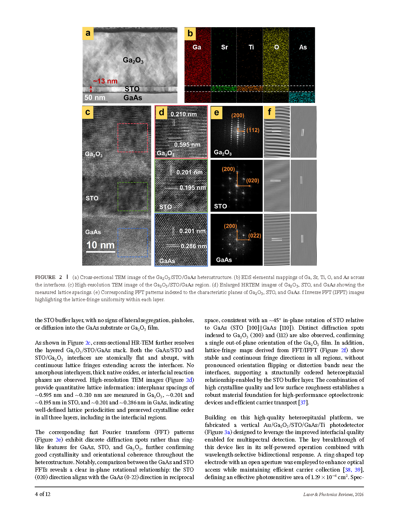
FIGURE 2. (a) Cross-sectional TEM image of the Ga₂O₃/STO/GaAs heterostructure. (b) EDS elemental mappings of Ga, Sr, Ti, O, and As across the interfaces. (c) High-resolution TEM image of the Ga₂O₃/STO/GaAs region. (d) Enlarged HRTEM images of Ga₂O₃, STO, and GaAs showing the measured lattice spacings. (e) Corresponding FFT patterns indexed to the characteristic planes of Ga₂O₃, STO, and GaAs. f Inverse FFT (IFFT) images highlighting the lattice-fringe uniformity within each layer.
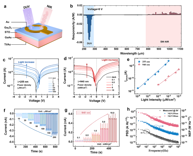
FIGURE 3. Photoresponse characteristics of the Au/Ga₂O₃/STO/GaAs/Ti photodetector. (a) Schematic device structure. (b) Spectral response from 200 to 1100 nm at zero bias, showing negative photocurrent in the DUV region and positive photocurrent in the NIR region. I–V characteristic under (c) 255 nm illumination (1–1000 µW cm²) and (d) 940 nm illumination (0.1–10 mW/cm2). (e) Photocurrent versus light intensity at 255 and 940 nm on log-log scale. Time-resolved photoresponse at zero bias under (f) 255 nm and (g) 940 nm illumination at various power densities. (h) Noise power spectral density (left axis) and noise equivalent power (right axis) as functions of frequency.
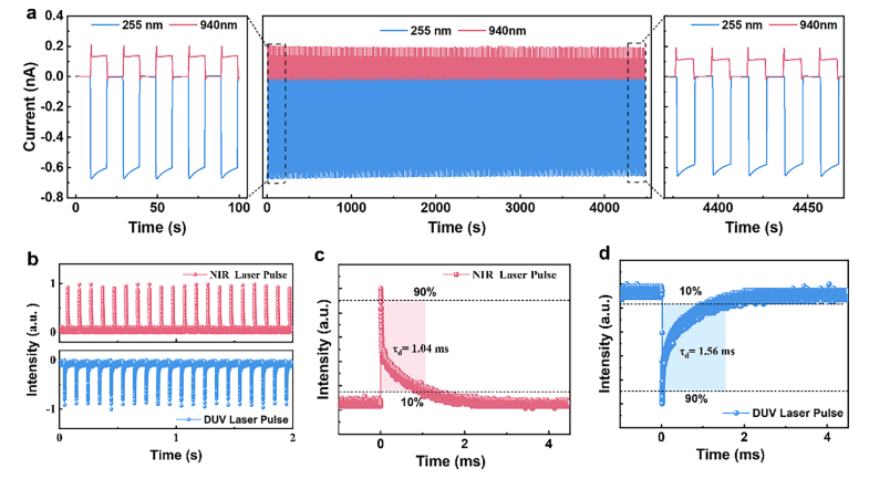
FIGURE 4. Dynamic response stability of the photodetector. (a) Long-term test under alternating 255 nm (200 µW cm²) and 940 nm (1 mW cm²) illumination 0.05 Hz for 4500 s. (b) Transient response 10 Hz pulsed laser excitation at 248 nm (DUV) and 1064 nm (NIR). Single-pulse response profiles showing decay times of (c) 1.04 ms for NIR and (d) 1.56 ms for DUV.
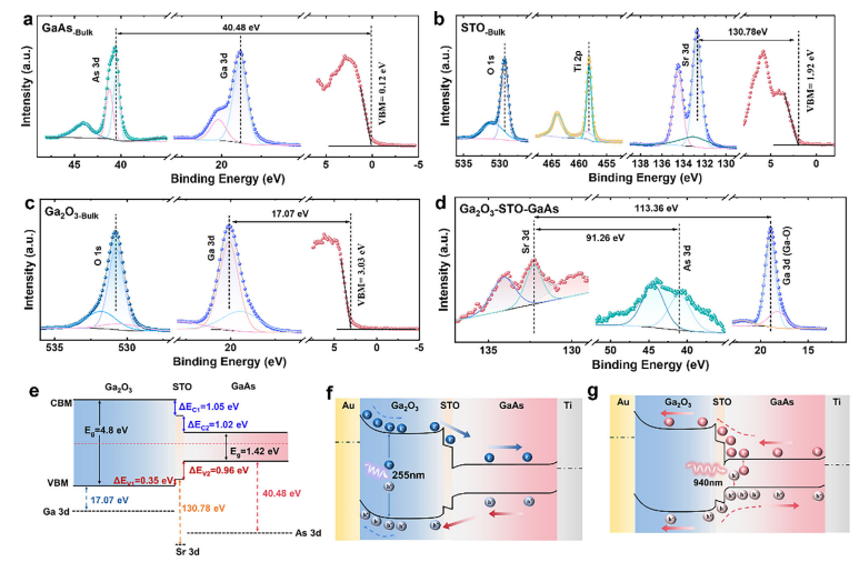
FIGURE 5. Band alignment analysis via XPS. (a–c) Core-level and valence band spectra of bulk (a) GaAs, (b) STO, and (c) Ga₂O₃. (d) Core-level spectra at the Ga₂O₃/STO/GaAs interface. (e) Schematic illustration of the energy band alignment for the Ga₂O₃/STO/GaAs heterojunction derived from XPS measurements. Band diagrams illustrating carrier transport mechanisms under (f) DUV and (g) NIR illumination.
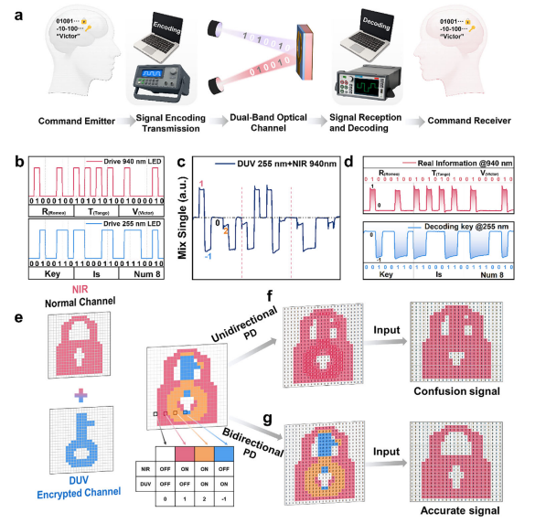
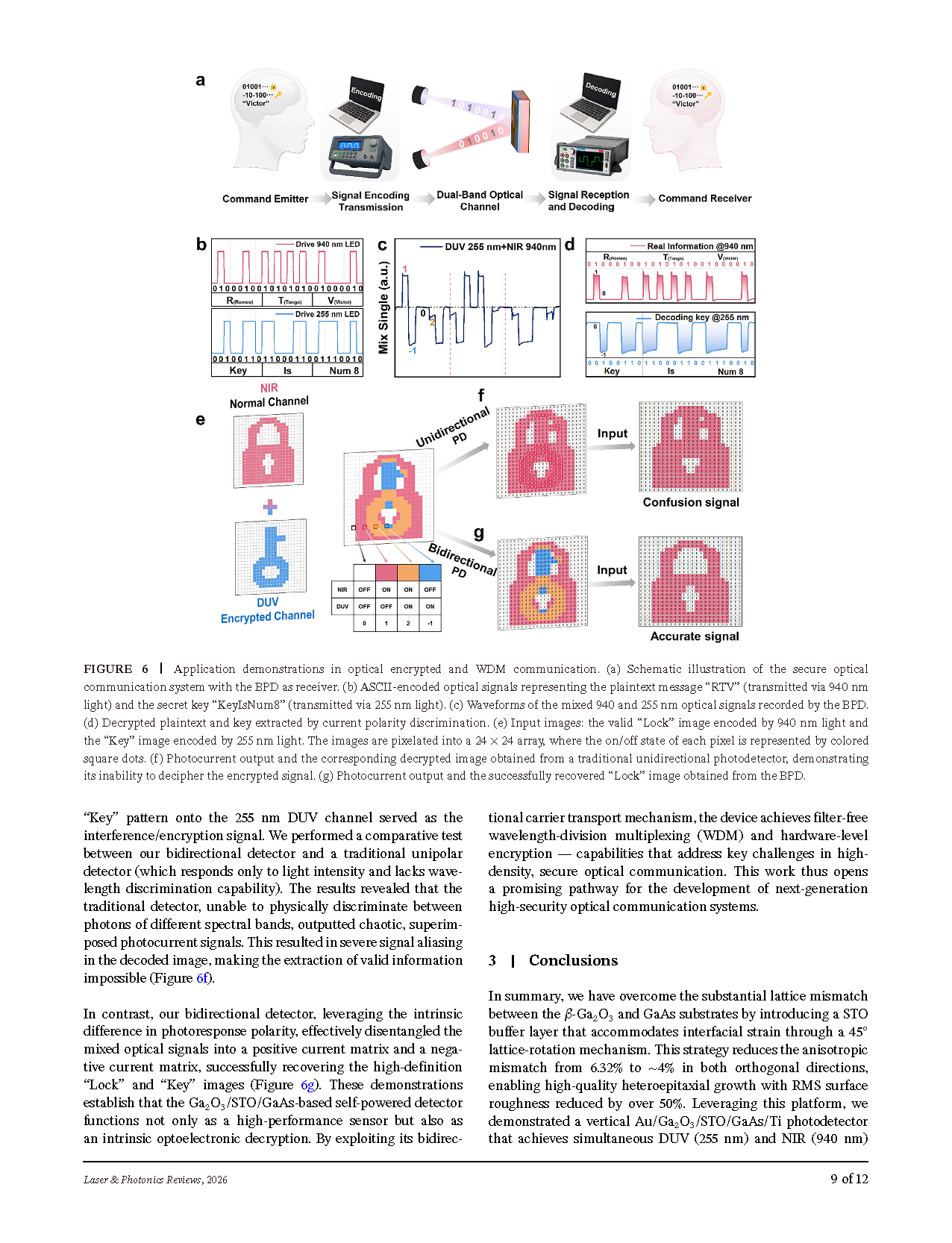
FIGURE 6. Application demonstrations in optical encrypted and WDM communication. (a) Schematic illustration of the secure optical communication system with the BPD as receiver. (b) ASCII-encoded optical signals representing the plaintext message “RTV” (transmitted via 940 nm light) and the secret key “KeyIsNum8” (transmitted via 255 nm light). (c) Waveforms of the mixed 940 and 255 nm optical signals recorded by the BPD. (d) Decrypted plaintext and key extracted by current polarity discrimination. (e) Input images: the valid “Lock” image encoded by 940 nm light and the “Key” image encoded by 255 nm light. The images are pixelated into a 24 × 24 array, where the on/off state of each pixel is represented by colored square dots. (f) Photocurrent output and the corresponding decrypted image obtained from a traditional unidirectional photodetector, demonstrating its inability to decipher the encrypted signal. (g) Photocurrent output and the successfully recovered “Lock” image obtained from the BPD.
DOI:
doi.org/10.1002/lpor.71239