Paper Sharing
【Member Papers】Microscopic origin of dopant-dependent defect states and carrier compensation in Si- and Sn-doped β-Ga₂O₃
日期:2026-05-11阅读:59
A research team led by Zhang Hongliang from Xiamen University, in collaboration with Zhang Zhaofu from Wuhan University, Qi Hongji from Shanghai Institute of Optics and Fine Mechanics, Chinese Academy of Sciences, the Shanghai Key Laboratory of Wide and Ultra-Wide Bandgap Semiconductor Materials, and Diamond Light Source, published a paper titled Microscopic origin of dopant-dependent defect states and carrier compensation in Si- and Sn-doped β-Ga2O3 in the journal Applied Physics Letters.
β-Ga2O3 is regarded as one of the most representative ultrawide-bandgap semiconductors due to its exceptionally high critical breakdown field and the capability for large-area bulk crystal growth via melt-based methods. These advantages make it highly promising for next-generation high-voltage power electronics with potential cost benefits over existing wide-bandgap materials. With the rapid development of industries such as electric vehicles, smart grids, rail transit, and 5G RF technologies, the demand for highly efficient and high-voltage power devices continues to increase, further enhancing the strategic importance of gallium oxide materials. As a fourth-generation ultrawide-bandgap semiconductor following SiC and GaN, gallium oxide has also been included in China’s “15th Five-Year Plan” strategic materials roadmap and is considered a key material platform for future power electronics and advanced semiconductor technologies.
As gallium oxide moves toward large-scale industrial applications, its industrial chain spans substrate growth, epitaxy, device fabrication, and system integration. Among these, epitaxial thin films serve as the critical bridge between upstream materials and downstream device realization. Their crystal quality, electrical controllability, and defect management capability directly determine the performance, stability, and reliability of Ga2O3 devices. However, the practical performance of current gallium oxide power devices still falls short of theoretical expectations, mainly due to two key bottlenecks: the high density of intrinsic defects and the extreme difficulty of achieving effective p-type doping. Since epitaxial layers act as the drift region in power devices, their crystalline quality and electrical properties strongly influence leakage current, breakdown strength, and long-term reliability. Doping remains the most direct and effective method for tuning carrier concentration in β-Ga2O3, while dopant activation efficiency and compensation behavior critically determine carrier transport properties. At the same time, doping-induced defect states can lead to carrier compensation, mobility degradation, and enhanced leakage current, becoming major limiting factors for device reliability.
To clarify the doping mechanisms and defect evolution behaviors in Ga2O3 epitaxial films, the research team combined high-resolution synchrotron radiation photoelectron spectroscopy with hybrid-functional first-principles calculations to systematically investigate how Si and Sn dopants modify the electronic structure of β-Ga2O3 and induce defect-state formation. This work provides important insight into the intrinsic relationship among doping, defects, and electronic structure, while also offering theoretical guidance for the precise control of Ga2O3 epitaxial films and the fabrication of high-performance devices.
The study revealed the formation behavior and electronic structure characteristics of substitutional donors, gallium vacancies, and donor–vacancy complex defects in Si- and Sn-doped β-Ga2O3. The results indicate that Si introduces shallower donor levels, making it more favorable for achieving higher dopant activation efficiency. In contrast, Sn forms deeper donor levels because the hybridization between Sn 4d and O 2p orbitals stabilizes neutral SnGa states. As the doping concentration increases, gallium vacancies (VGa) gradually become the dominant acceptor-type compensation defects. Under oxygen-rich conditions, Sn is more likely than Si to form stable SnGa–VGa complex defects, indicating that Sn-doped systems are more susceptible to self-compensation effects. Electronic structure analysis further shows that Sn doping more readily introduces localized in-gap defect states, whereas Si doping preserves more delocalized bonding characteristics. These findings demonstrate that donor–vacancy coupling and orbital hybridization behaviors are the key mechanisms governing doping compensation effects and defect-state evolution in β-Ga2O3.
This work provides important theoretical support for efficient doping strategies and the understanding of defect-related electronic states in gallium oxide thin films.
The paper was jointly authored by teams from Xiamen University, Wuhan University, Shanghai Institute of Optics and Fine Mechanics, Chinese Academy of Sciences, the Shanghai Key Laboratory of Wide and Ultra-Wide Bandgap Semiconductor Materials, and Diamond Light Source. The co-first authors are Sheng Ziqian, a 2021 PhD student at Xiamen University, and Liu Taiqiao, a 2023 PhD student at Wuhan University, whose research focuses on the electronic structure, defects, and doping-related theoretical calculations of gallium oxide epitaxial films. The research was supported by China’s National Key R&D Program and the National Natural Science Foundation of China.
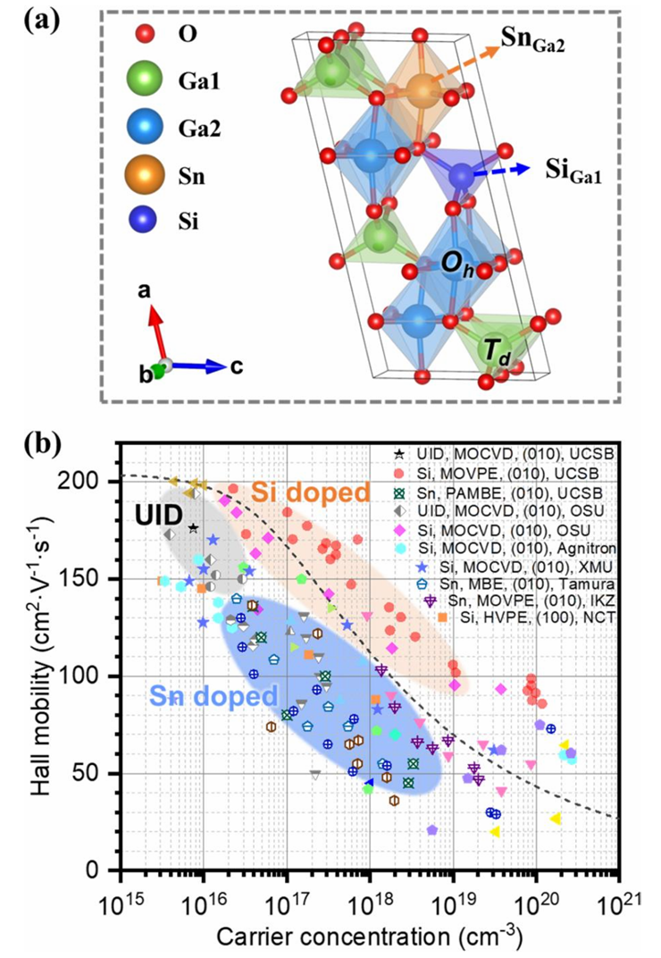
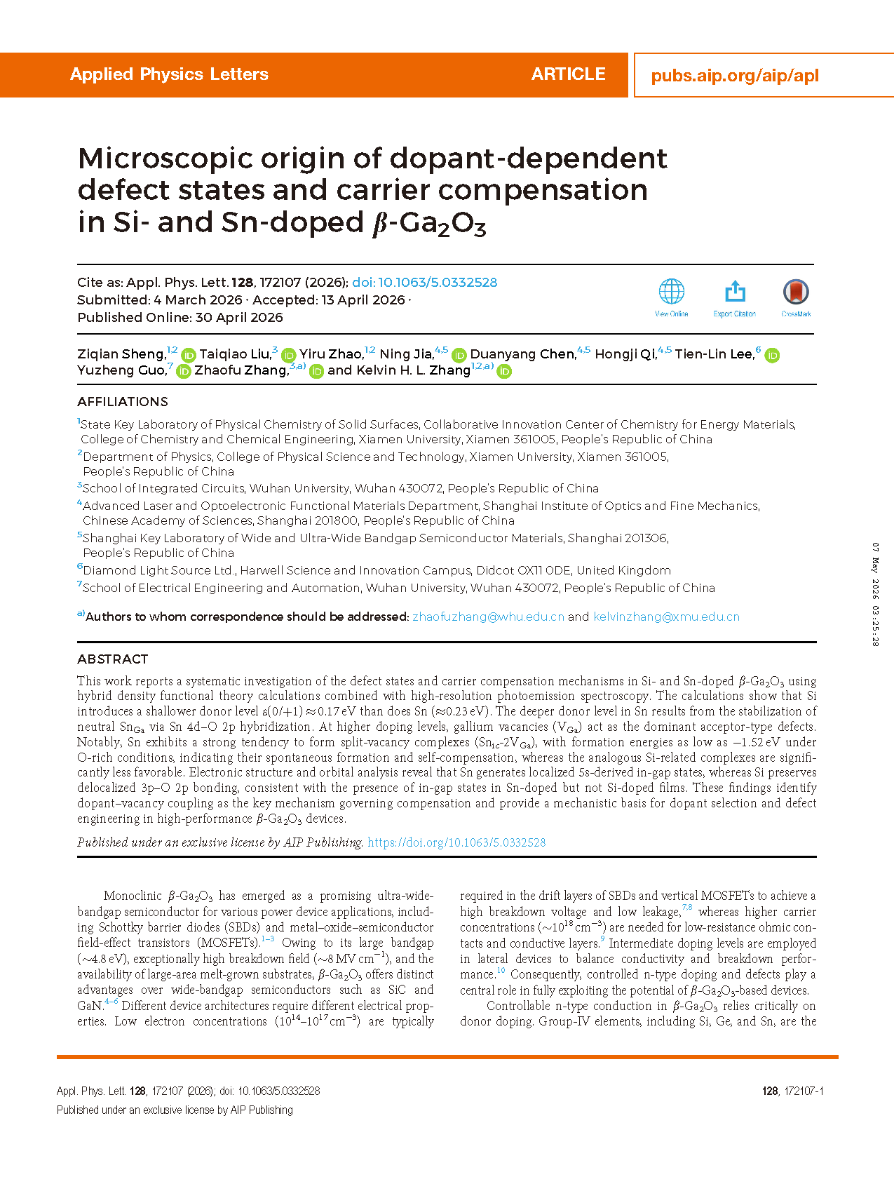
Fig. 1 (a) Crystal structure of β-Ga2O3, where Si occupies the tetrahedral Ga1 site and Sn occupies the octahedral Ga2 site; and (b) the reported Hall mobilities of UID (gray), Si-doped (orange), and Sn-doped (blue) Ga2O3 thin films as a function of carrier concentrations reported in Refs. S1–S33 in the supplementary material.
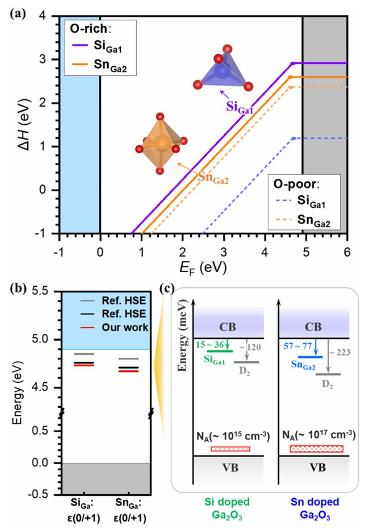
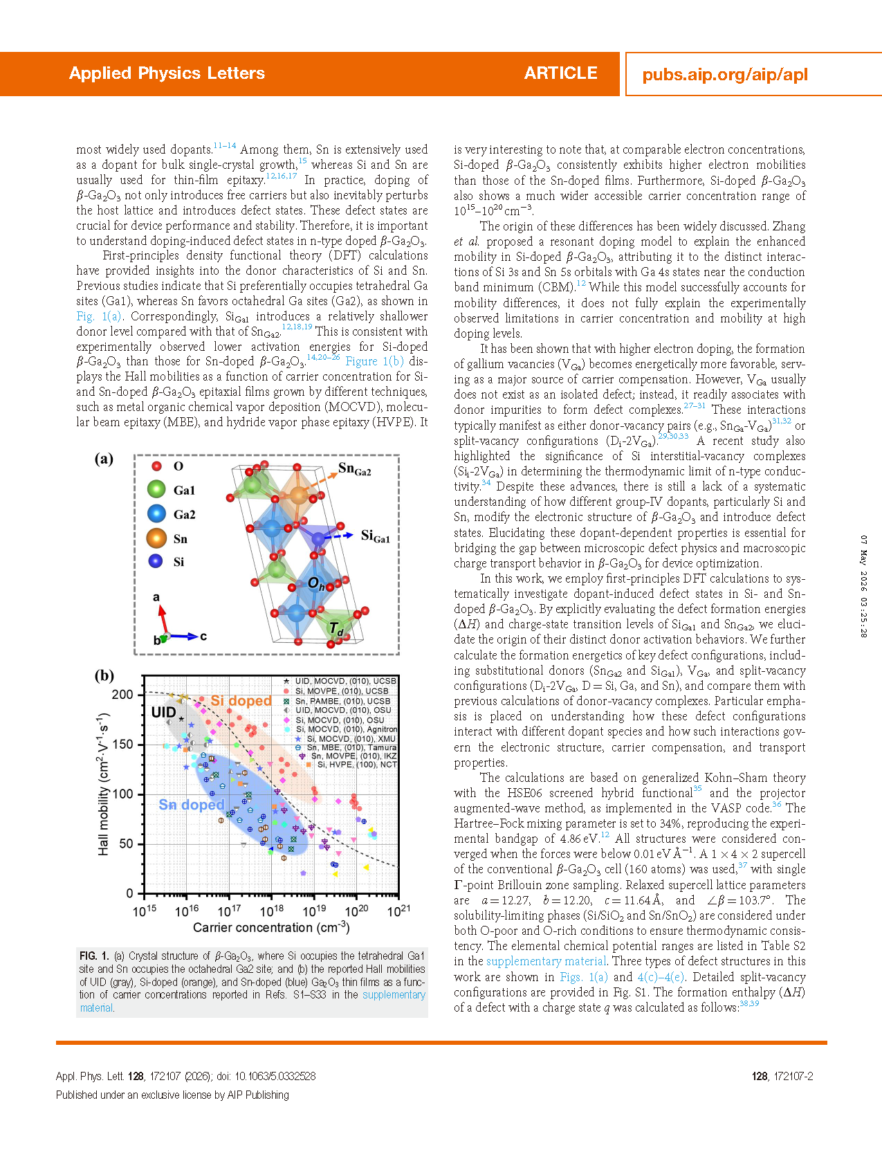
Figure 2. (a) Formation enthalpies (ΔH) of SnGa2 and SiGa1 under O-rich and O-poor conditions; (b) comparison of the transition levels ε(0/+1) of SnGa2 and SiGa1 between this work and the reported values; and (c) schematic illustration of reported donor activation energies for Si and Sn in β-Ga2O3. A secondary donor level D2 for the Si-doped and Sn-doped Ga2O3 thin films is included.
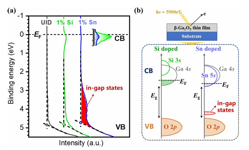
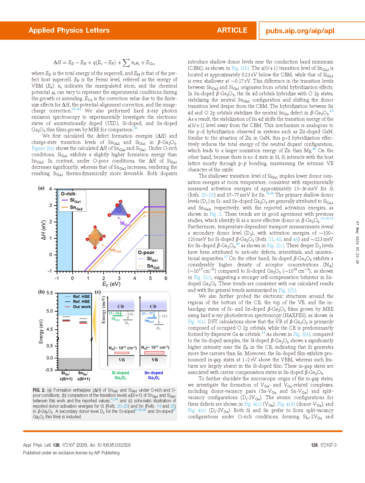
Figure 3. (a) The CB and VB spectra of UID β-Ga2O3, Si-doped, and Sn-doped Ga2O3 thin films measured by HAXPES excited with photon energy of 5900 eV; and (b) schematic illustration of the CB and VB electronic structures.
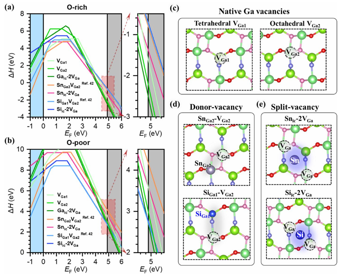
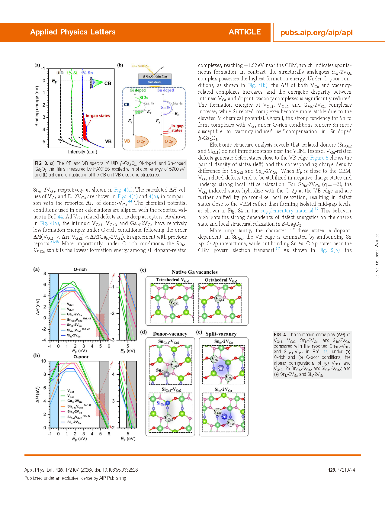
Figure 4. The formation enthalpies (ΔH) of VGa1, VGa2, Snic-2VGa and Siic-2VGa compared with the reported SnGa2-VGa2 and SiGa1-VGa2 in Ref. 44, under (a) O-rich and (b) O-poor conditions; the atomic configurations of (c) VGa1 and VGa2 (d) SnGa2-VGa2 and SiGa1-VGa2; and (e) Snic-2VGa and Siic-2VGa.
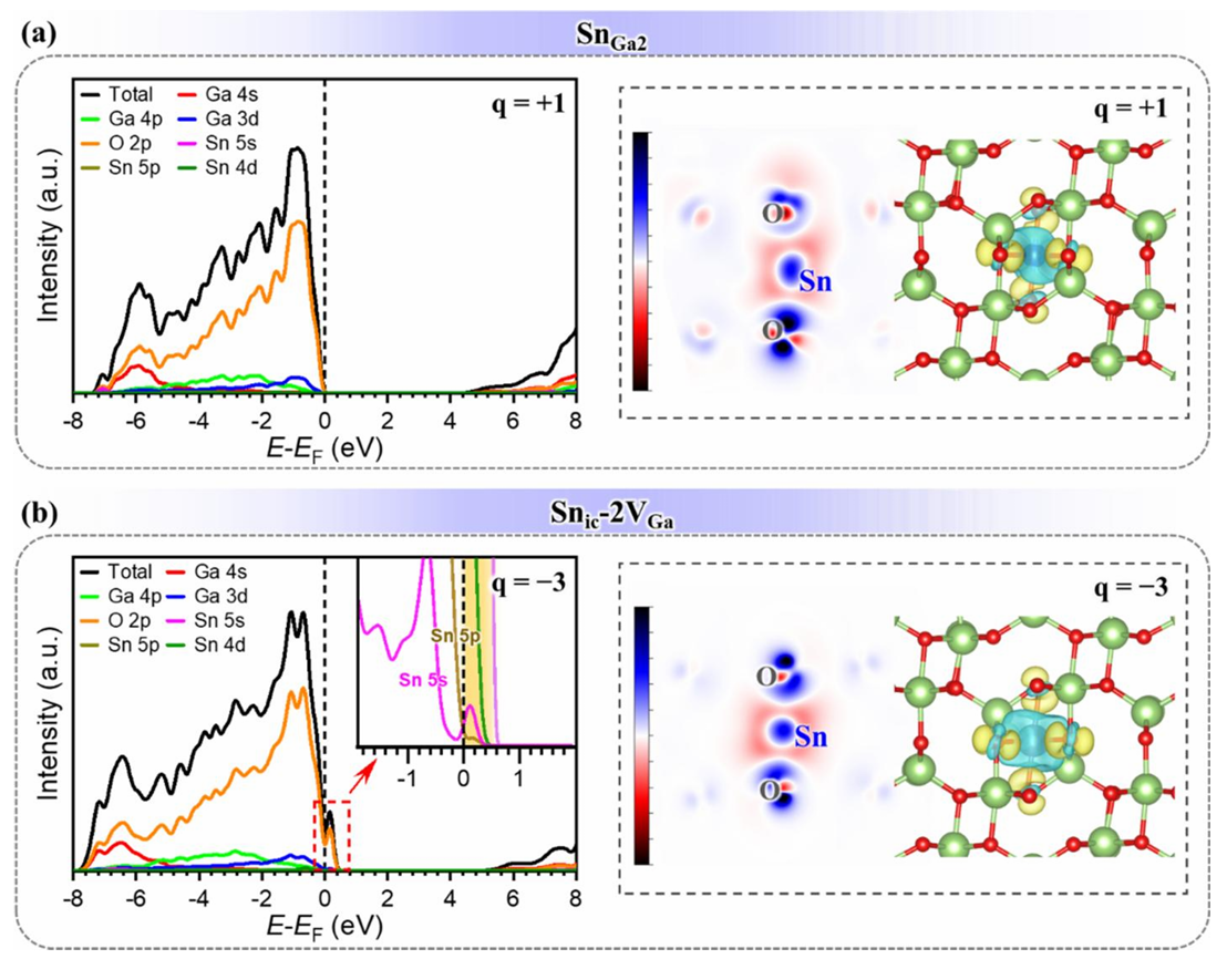
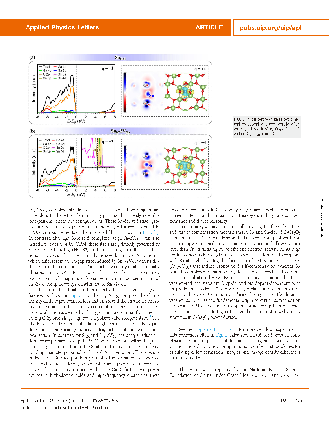
Figure 5. Partial density of states (left panel) and corresponding charge density differences (right panel) of (a) SnGa2 (q=+1) and (b) Snic-2VGa (q=-3).
DOI:
doi.org/10.1063/5.0332528