Paper Sharing
【Domestic Papers】Deformation and material removal mechanisms of single-crystal β-Ga₂O₃ via deep-ultraviolet-assisted surface corrosion
日期:2026-05-11阅读:43
Researchers from the Sun Yat-Sen University have published a dissertation titled " Deformation and material removal mechanisms of single-crystal β‑Ga₂O₃ via deep-ultraviolet-assisted surface corrosion" in Applied Surface Science.
Background
Ultra-wide bandgap semiconductor gallium oxide (Ga2O3) has emerged as a highly promising material for next-generation electronic and optoelectronic applications owing to its exceptional intrinsic properties, including a large bandgap, high breakdown electric field, excellent thermal and chemical stability, and comparatively low crystal growth cost. These advantages position Ga2O3 as a strong candidate for high-power electronics, radio-frequency devices, and deep-ultraviolet optoelectronics, with substantial potential to support future developments in information technology, energy systems, and defense-related applications. Because device performance is critically dependent on substrate surface quality, achieving ultra-smooth and damage-free Ga2O3 wafers is a prerequisite for reliable device fabrication and integration.
Abstract
Efficient, low-damage machining of single-crystal β‑Ga₂O₃ is severely constrained by its high hardness and intrinsic brittleness. In this work, deep ultraviolet (DUV) irradiation–assisted corrosion is proposed as a surface modification strategy to regulate deformation and material removal behavior under contact loading. DUV irradiation at 185 nm significantly enhances alkaline corrosion, promoting surface hydroxylation and inducing pronounced softening of the near-surface region. Nanoindentation and nanoscratch tests reveal that DUV-assisted corroded surfaces exhibit reduced hardness and elastic modulus, lower and more stable lateral forces, reduced friction coefficients, and increased material removal depth and volume under identical normal loads, indicating a transition toward ductile-dominated removal. Cross-sectional transmission electron microscopy confirms a continuous amorphous surface layer of ~ 18 nm formed beneath scratch grooves, which accommodates plastic deformation and suppresses subsurface cracking. In contrast, DUV-free and pristine surfaces exhibit limited amorphization and pronounced brittle damage. Quantitative agreement between experimentally measured and modeled volumetric removal further validates that the enhanced removal efficiency originates from controlled surface softening rather than brittle fracture. These results demonstrate that DUV irradiation–assisted corrosion fundamentally alters the deformation and material removal behaviour of β‑Ga₂O₃ , providing an effective pathway for stable, low-load, and low-damage ultra-precision machining.
Highlights
A 185 nm DUV-assisted alkaline corrosion strategy is proposed, which significantly enhances surface hydroxylation and near-surface softening of β‑Ga₂O₃.
DUV-assisted corrosion transforms the material removal of β‑Ga₂O₃ from brittle fracture-dominated to stable plastic deformation-dominated and suppresses subsurface damage.
It is revealed that the ~18 nm continuous amorphous surface layer regulated by DUV is the core mechanism for low-damage ultra-precision machining of β‑Ga₂O₃.
Conclusion
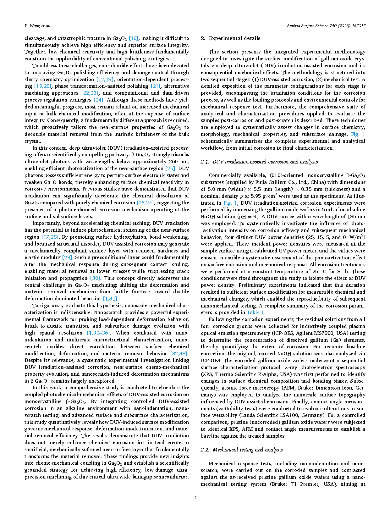
Overall, this work demonstrates that DUV irradiation-assisted corrosion is not merely a chemical etching process but an effective surface engineering strategy that tailors the near-surface mechanical response of β‑Ga₂O₃. By introducing a controlled, sacrificial softened layer, this approach raises brittle-to-ductile transition threshold and expands the machining window. These findings provide fundamental insight into photo-chemo-mechanical coupling in gallium oxide and offer a practical approach toward efficient, stable, and low-damage ultra-precision machining of this technologically important wide-bandgap oxide material.
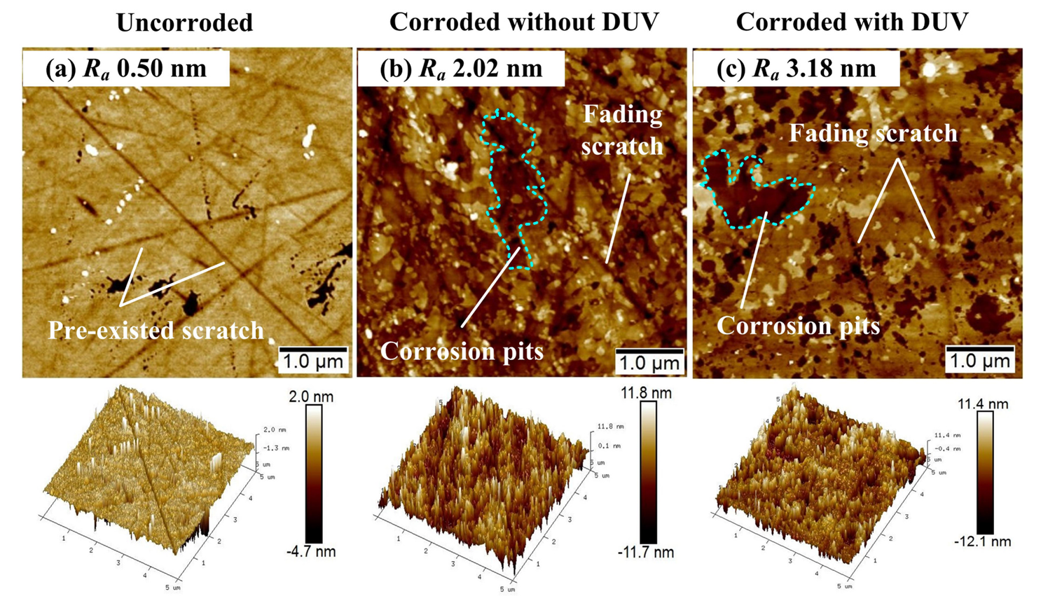
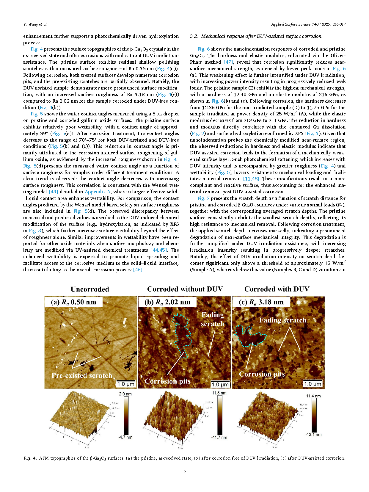
Fig. 1 AFM topographies of the β‑Ga₂O₃ surfaces: (a) the pristine, as-received state, (b) after corrosion free of DUV irradiation, (c) after DUV-assisted corrosion.
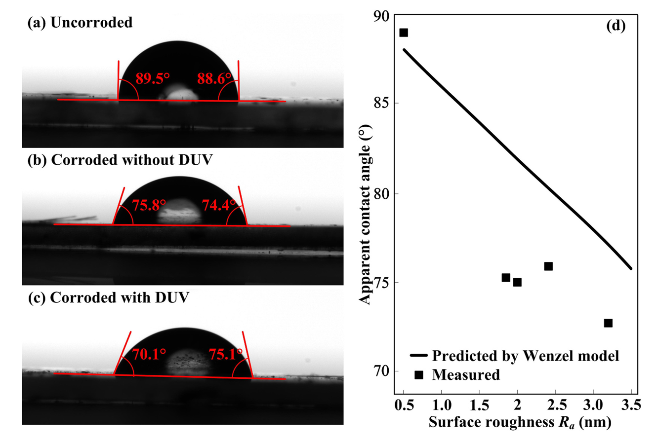
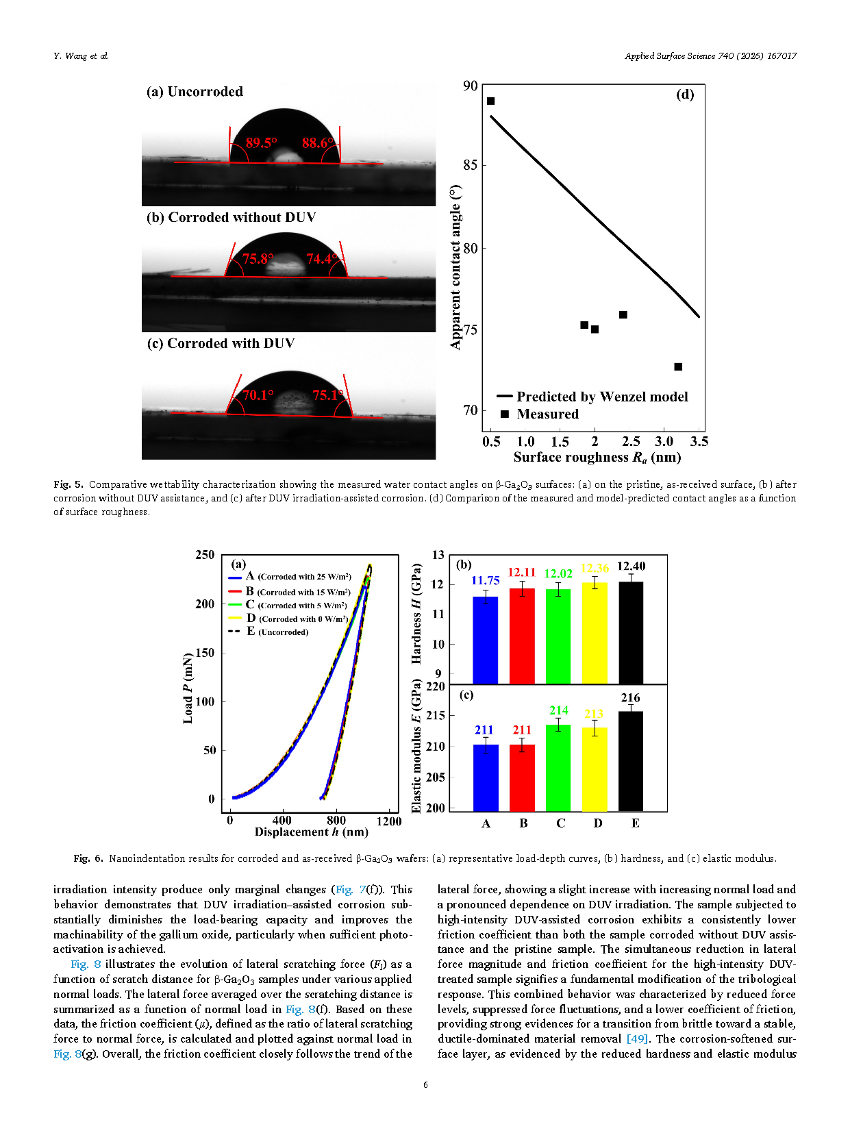
Figure 2. Comparative wettability characterization showing the measured water contact angles on β‑Ga₂O₃ surfaces: (a) on the pristine, as-received surface, (b) after corrosion without DUV assistance, and (c) after DUV irradiation-assisted corrosion. (d) Comparison of the measured and model-predicted contact angles as a function of surface roughness.
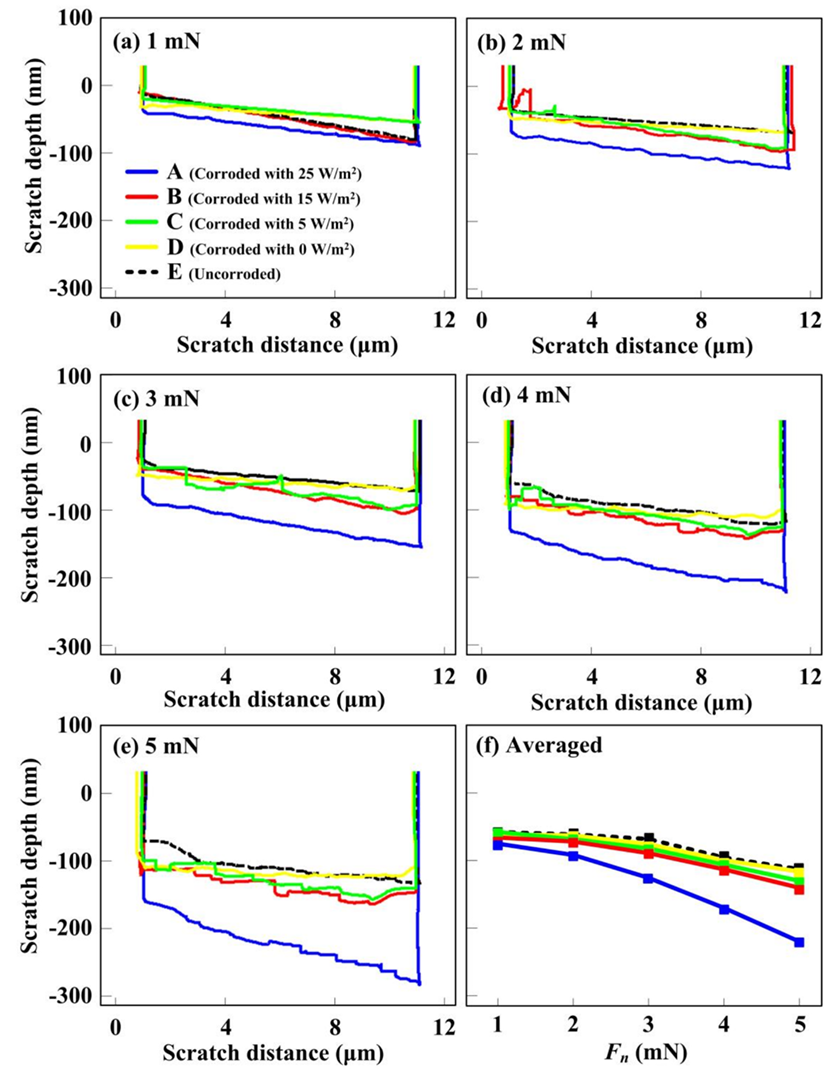
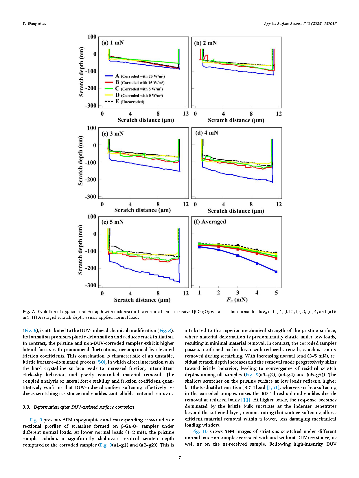
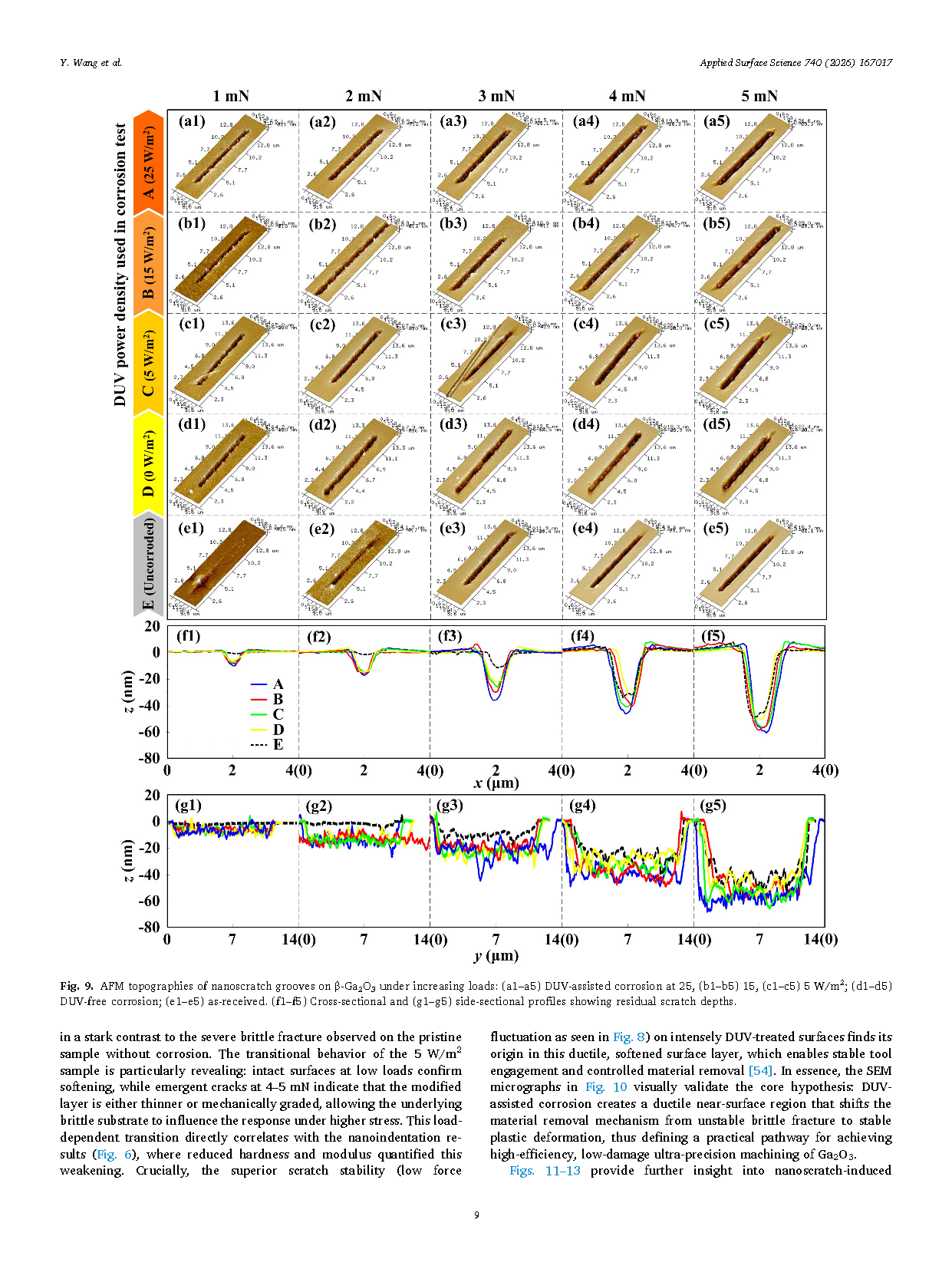
Figure 3. Evolution of applied scratch depth with distance for the corroded and as-received β‑Ga₂O₃ wafers under normal loads Fₙ of (a) 1, (b) 2, (c) 3, (d) 4, and (e) 5 mN. (f) Averaged scratch depth versus applied normal load.
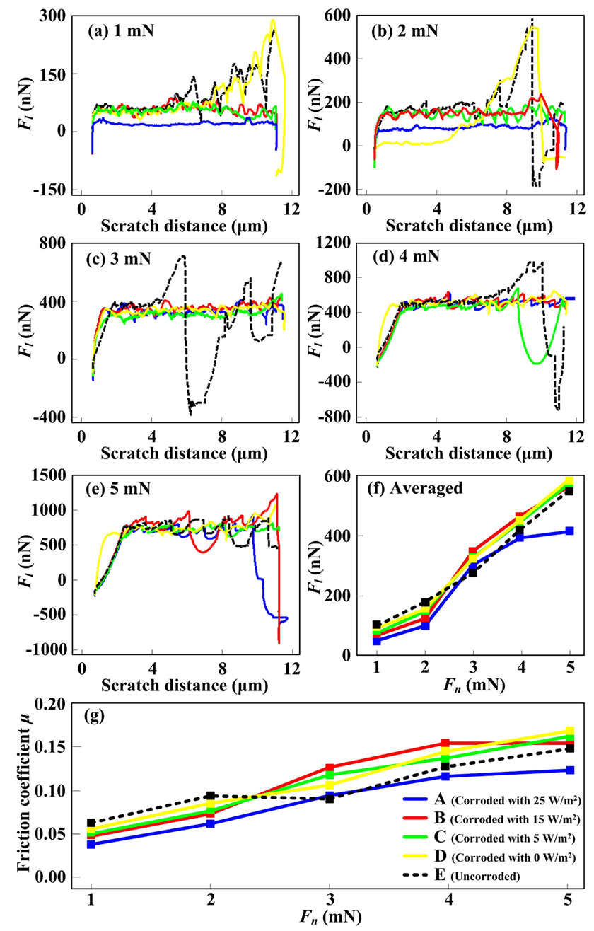
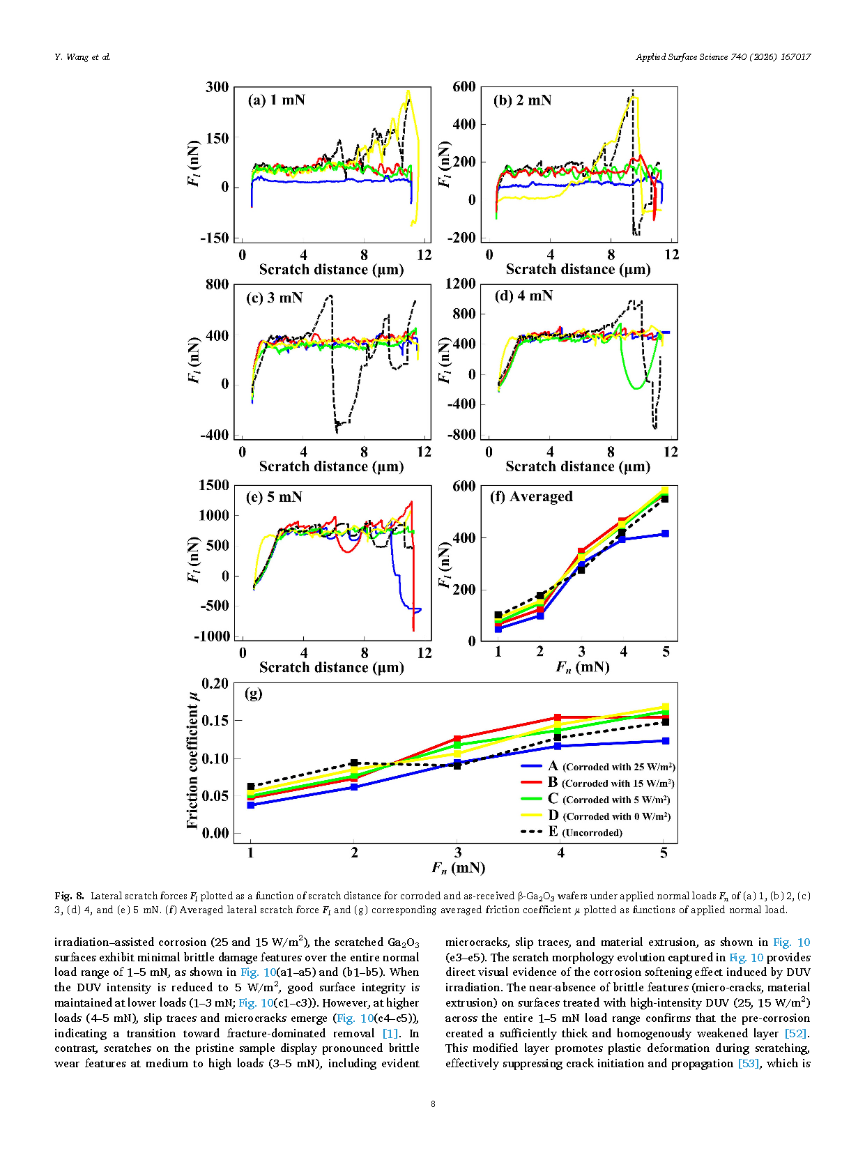
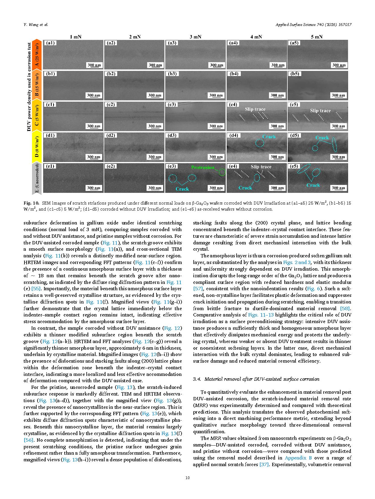
Figure 4. Lateral scratch forces Fₗ plotted as a function of scratch distance for corroded and as-received β‑Ga₂O₃ wafers under applied normal loads Fn of (a) 1, (b) 2, (c) 3,(d) 4, and (e) 5 mN. (f) Averaged lateral scratch force F1 and (g) corresponding averaged friction coefficient μ plotted as functions of applied normal load.
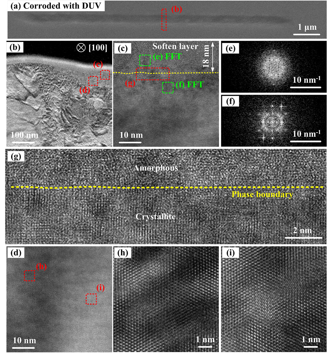
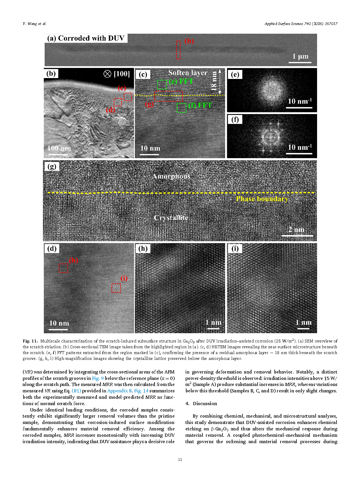
Figure 5. Multiscale characterization of the scratch-induced subsurface structure in Ga2O3 after DUV irradiation-assisted corrosion (25 W/m²). (a) SEM overview of the scratch striation. (b) Cross-sectional TEM image taken from the highlighted region in (a). (c, d) HRTEM images revealing the near-surface microstructure beneath the scratch. (e, f) FFT patterns extracted from the region marked in (c), confirming the presence of a residual amorphous layer ~ 18 nm thick beneath the scratch groove. (g, h, i) High-magnification images showing the crystalline lattice preserved below the amorphous layer.
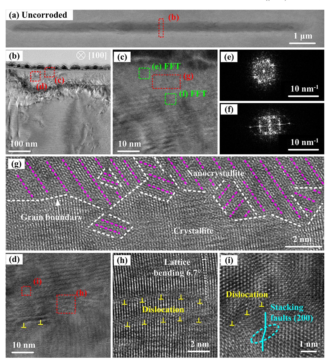
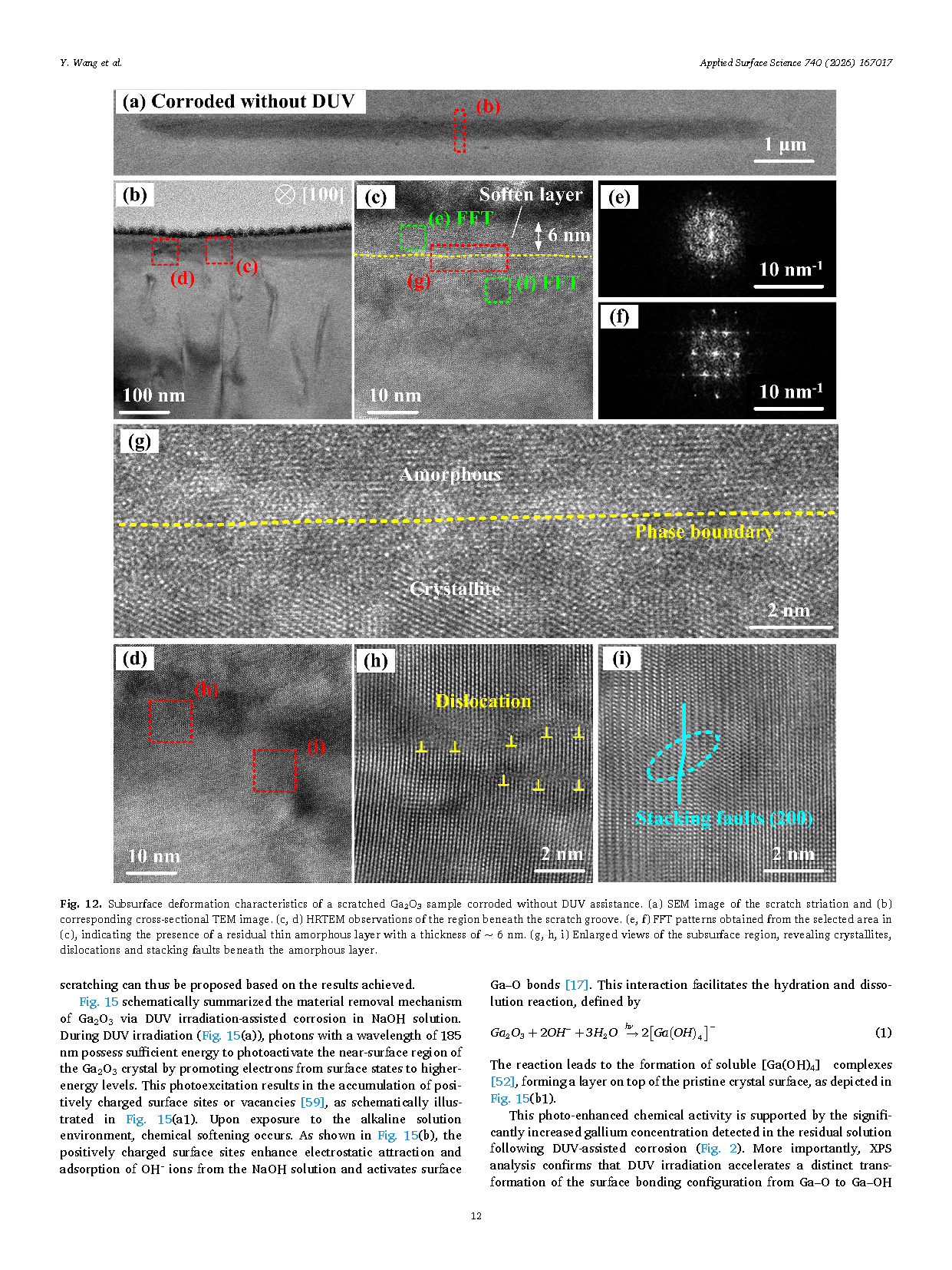
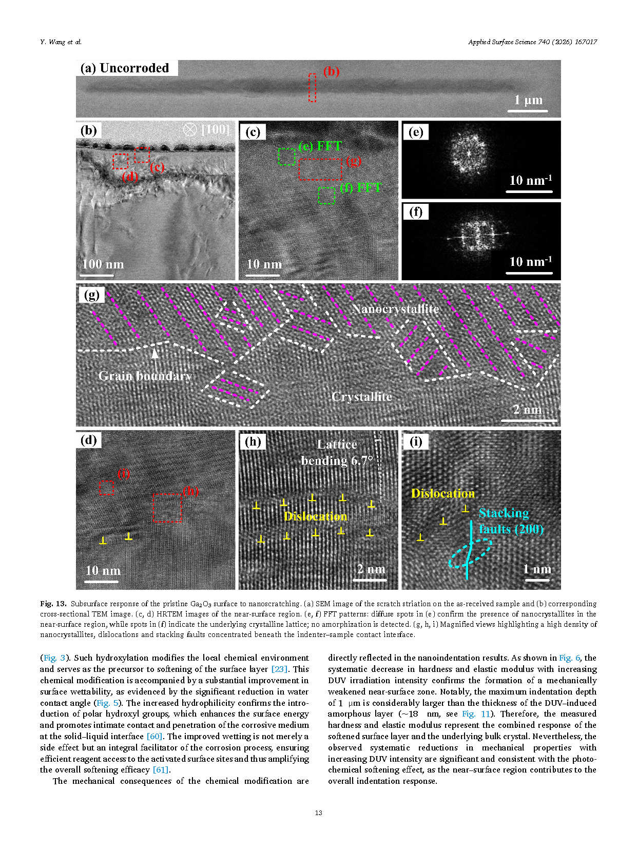
Figure 6. Subsurface response of the pristine Ga2O3 surface to nanoscratching. (a) SEM image of the scratch striation on the as-received sample and (b) corresponding cross-sectional TEM image. (c, d) HRTEM images of the near-surface region. (e, f) FFT patterns: diffuse spots in (e) confirm the presence of nanocrystallites in the near-surface region, while spots in (f) indicate the underlying crystalline lattice; no amorphization is detected. (g, h, i) Magnified views highlighting a high density of nanocrystallites, dislocations and stacking faults concentrated beneath the indenter–sample contact interface.
DOI:
doi.org/10.1016/j.apsusc.2026.167017