Paper Sharing
【Member Papers】Interface-engineered Ga₂O₃ photodetectors with quantum-dot-assisted band modulation for spectrum-selective UVC detection
日期:2026-05-08阅读:47
Researchers from the Xidian University, Fudan University and Northwestern Polytechnical University have published a dissertation titled " Interface-engineered Ga2O3 photodetectors with quantum-dot-assisted band modulation for spectrum-selective UVC detection" in Materials Today Electronics.
Background
Ultraviolet-C (UVC, 200–280 nm) photodetectors are widely used in flame detection, environmental monitoring, secure optical communication, solar-blind imaging, quantum photonics and autonomous sensing. With the development of related fields, UVC detectors are required to achieve high responsivity and millisecond-level temporal response under ultra-weak illumination. However, traditional wide-bandgap semiconductors such as ZnO, AlGaN and diamond have problems such as complex epitaxy, high defect density and limited carrier transport, which restrict the simultaneous optimization of sensitivity and response speed. As an emerging wide-bandgap semiconductor material, Ga₂O₃ has a band gap of 4.9–5.2 eV, good thermal and chemical stability, and intrinsic solar-blind response characteristics, making it an ideal material for UVC photodetectors. Nevertheless, the intrinsic n-type conductivity and doping asymmetry of Ga₂O₃ hinder the fabrication of high-efficiency p-n junctions, resulting in low carrier extraction efficiency in Schottky and MSM photodetectors. Constructing heterojunctions with p-type semiconductors can introduce built-in electric fields and adjustable band offsets, which is an effective way to solve the above problems. However, the existing Ga₂O₃-based heterojunction photodetectors still have high dark current and slow photoresponse due to interface recombination and trap-assisted carrier dynamics.
Abstract
Achieving fast and highly sensitive ultraviolet-C (UVC) detection under ultra-weak illumination remains challenging due to inefficient carrier separation and severe interfacial recombination in wide-bandgap semiconductors. Here, the team reports an interface-engineered Ga₂O₃-based photodetector by integrating p-type NiO quantum dots (p-NQDs) onto an n-type Ga₂O₃ channel to form a surface-type heterojunction. The introduction of the p-NQDs modifies the interfacial energy landscape, leading to enhanced built-in electric fields and suppressed recombination at the Ga₂O₃ surface. Benefiting from the type-II band alignment and interfacial modulation, the heterojunction device achieves an ultralow dark current of ~10⁻¹⁴ A, a high responsivity of 4.66 A/W, and a detectivity of 5.56 × 10¹⁴ Jones under 254 nm illumination. Time-resolved measurements reveal a significantly accelerated photoresponse with rise and decay times down to tens of milliseconds, indicating improved carrier transport dynamics compared with pristine Ga₂O₃ devices. Furthermore, a proof-of-concept single-pixel UVC imaging demonstration confirms high-contrast spatial mapping capability under weak illumination. These results suggest that quantum-dot-assisted interfacial engineering provides an effective strategy for modulating carrier dynamics in oxide semiconductors, offering insights for the development of high-sensitivity solar-blind UVC photodetectors.
Highlights
Propose a quantum-dot-mediated surface heterojunction strategy for Ga₂O₃-based UVC photodetectors by selectively integrating p-type NiO quantum dots onto n-type Ga₂O₃ channel.
Realize type-II band alignment at p-NQDs/n-Ga₂O₃ interface, which enhances built-in electric field, suppresses interfacial recombination and improves carrier separation efficiency.
Obtain ultra-low dark current (~10⁻¹⁴ A), high responsivity (4.66 A/W), high detectivity (5.56 × 10¹⁴ Jones) and millisecond-level response speed (rise time 24 ms, decay time 8 ms) under 254 nm illumination.
Complete proof-of-concept single-pixel UVC spatial mapping with high contrast under weak illumination, verifying the imaging application potential.
Conclusion
The team reports an interface-engineered p-NQDs/n-Ga₂O₃ photodetector that achieves enhanced performance in the solar-blind UVC region through interface modulation enabled by type-II band alignment. The incorporation of p-NQDs modifies the interfacial electronic structure and provides defect passivation, facilitating carrier separation and suppressing recombination losses. As a result, the device exhibits a high responsivity of 4.66 A/W, a specific detectivity of 5.56 × 10¹⁴ Jones, and a fast response with rise and decay times of 24 ms and 8 ms, respectively, under 254 nm illumination. Furthermore, a proof-of-concept single-point UVC spatial mapping demonstration reveals clear pattern recognition with high contrast under low-intensity illumination, highlighting the potential of the device for spatial light discrimination. These results underscore the effectiveness of interface engineering using quantum dots as an approach for tuning carrier dynamics in Ga₂O₃-based heterostructures. This work provides insights into the design of low-dark-current, high-sensitivity solar-blind UVC photodetectors and suggests a promising pathway toward advanced deep-UV sensing and imaging applications.
Project Support
National Natural Science Foundation of China (Grant No. 62404176, 62293522, 12175298), National Key R&D Program of China (No. 2024YFF1504400), Zhejiang Provincial Natural Science Foundation of China (LDT23F0402, LDT23F04024F04), Leading innovation and entrepreneurship Project of Zhejiang Province (2023R01014), the key program of Shannxi Provincial Department of science and technology support (2024CY2-GJHX-81).
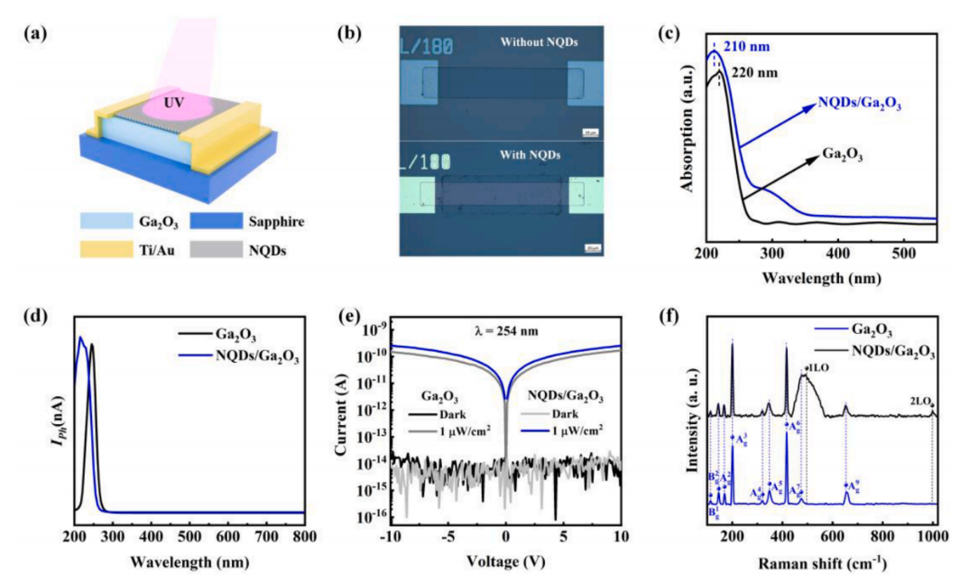
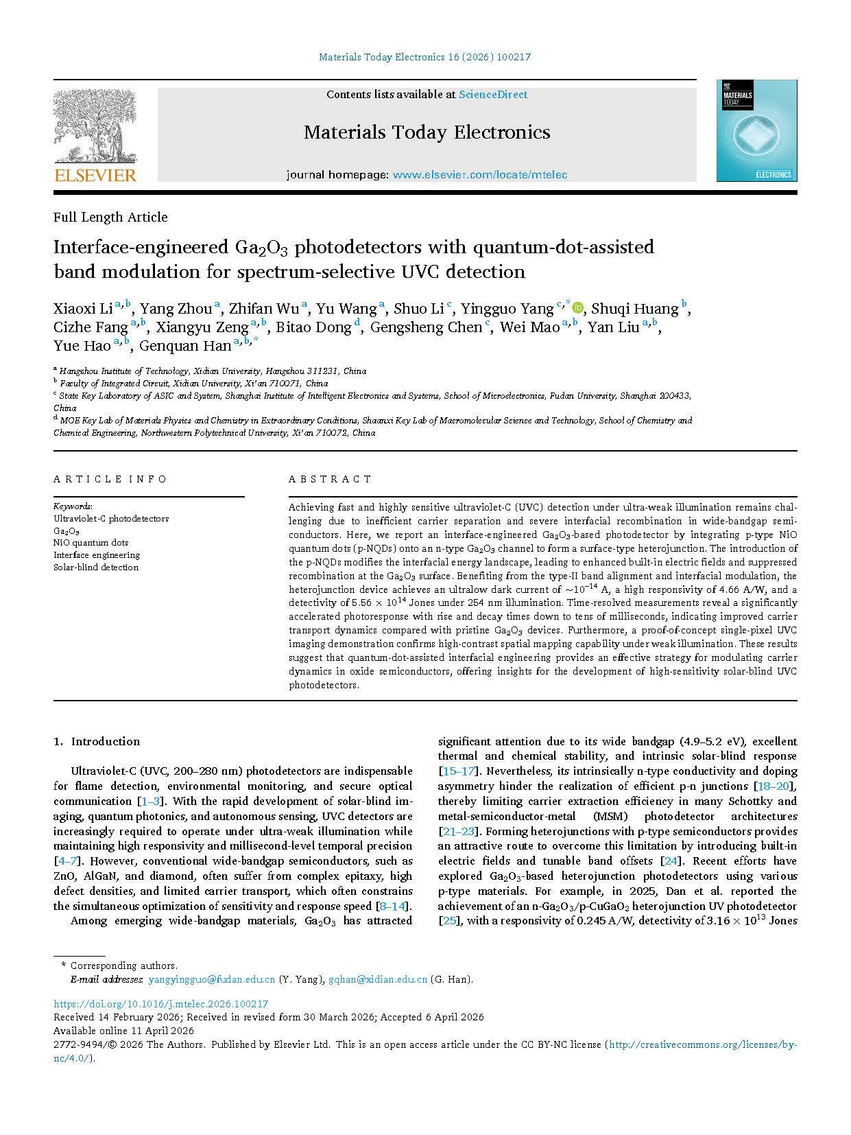
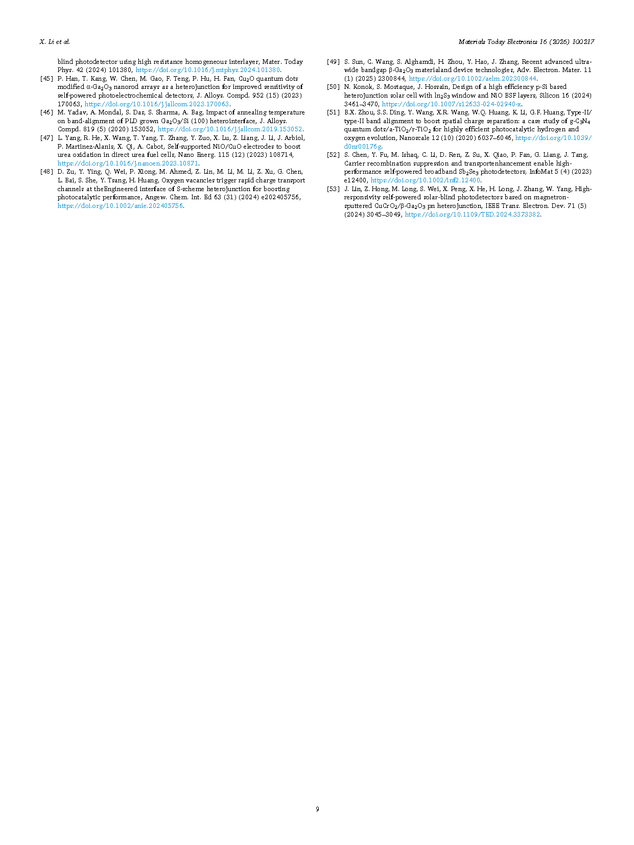
Fig. 1 (a) Schematic illustration of the p-NQDs/n-Ga₂O₃ photodetector under UV light illumination. (b) Optical microscope images of the fabricated Ga₂O₃ photodetector without (top) and with (bottom) p-NQDs coating. (c) UV-Vis absorption spectra of bare Ga₂O₃ and p-NQDs/n-Ga₂O₃ heterostructures. (d) Spectral photocurrent responses of the two devices, showing enhanced responsivity in the UVC region for the heterojunction. (e) Semi-log I-V characteristics under dark and 254 nm UV illumination at 1 μW/cm², comparing Ga₂O₃ and p-NQDs/n-Ga₂O₃ devices. (f) Raman spectra of Ga₂O₃ and p-NQDs/n-Ga₂O₃ revealing additional peaks attributed to the phonon modes of p-NQDs.
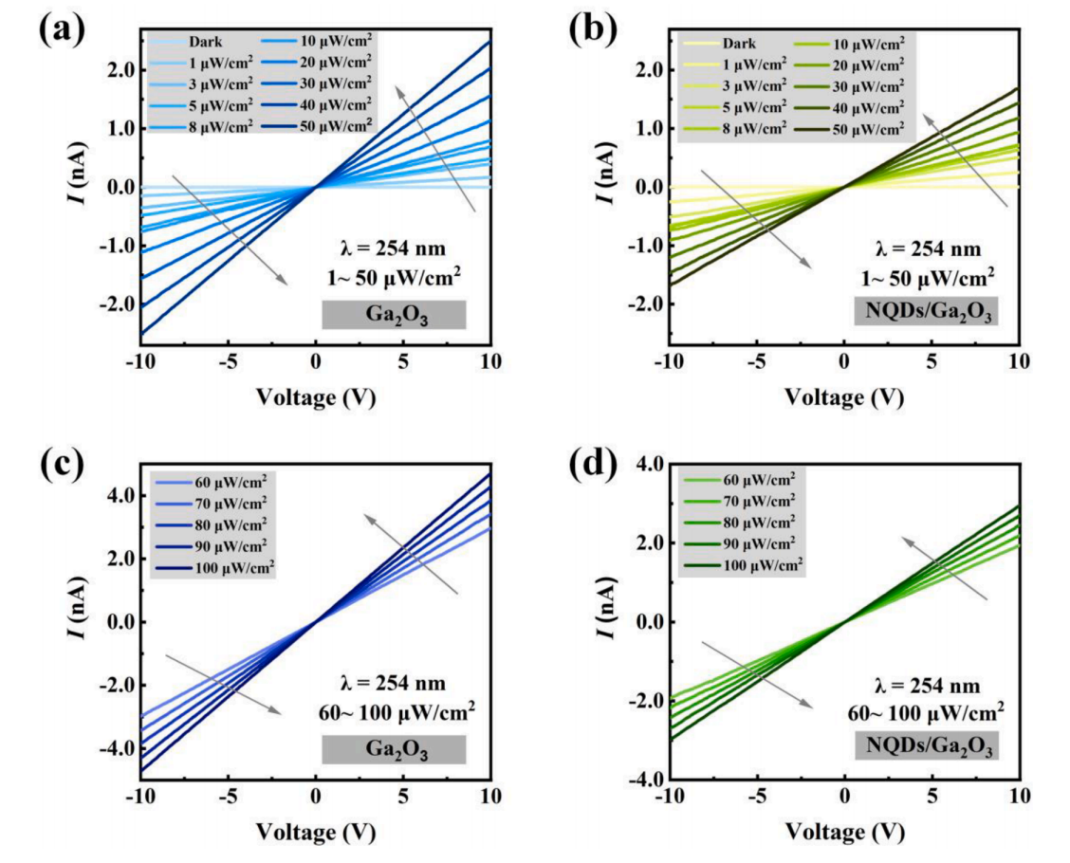
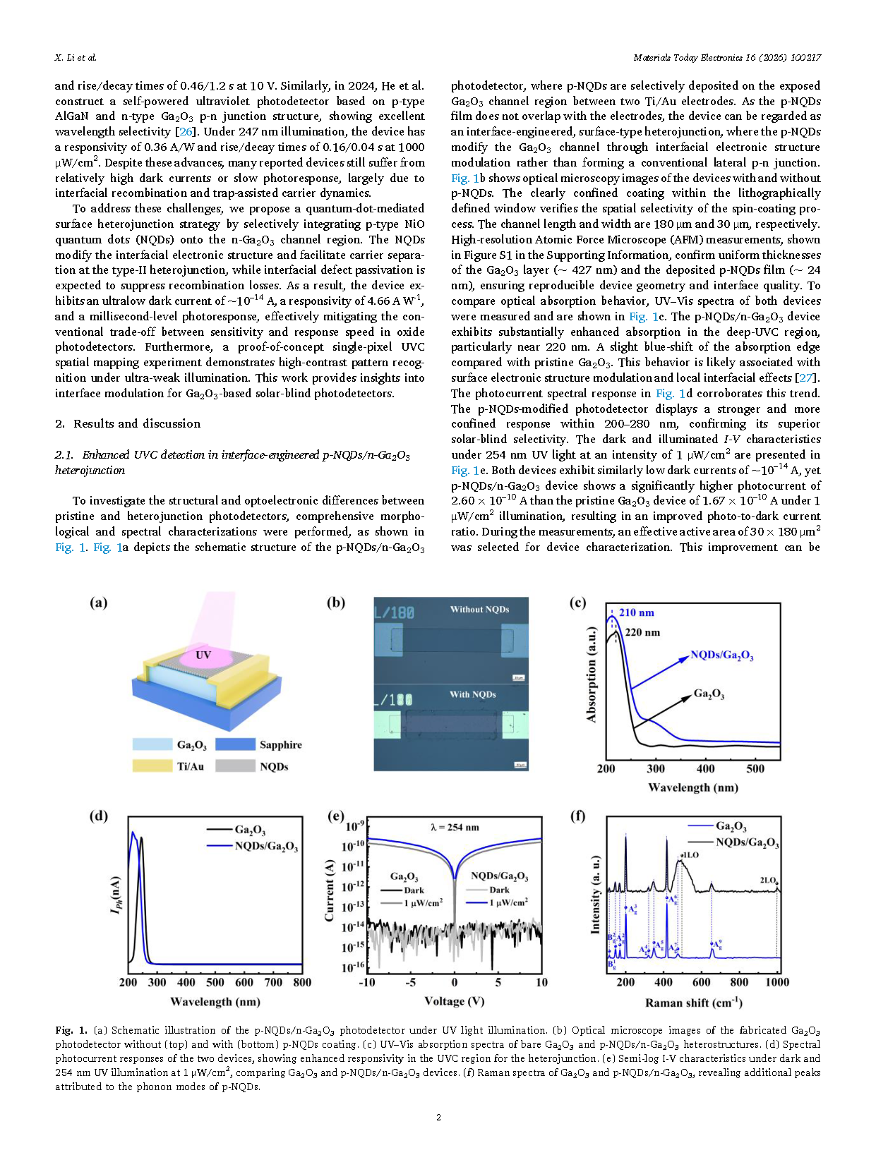
Fig. 2 (a-b) I-V curves of the Ga₂O₃ photodetector without/with p-NQDs in the dark and under 254 nm illumination with intensities from 1 to 50 µW/cm². (c-d) I-V curves of the Ga₂O₃ photodetector without/with p-NQDs under 254 nm illumination with intensities from 60 to 100 µW/cm².
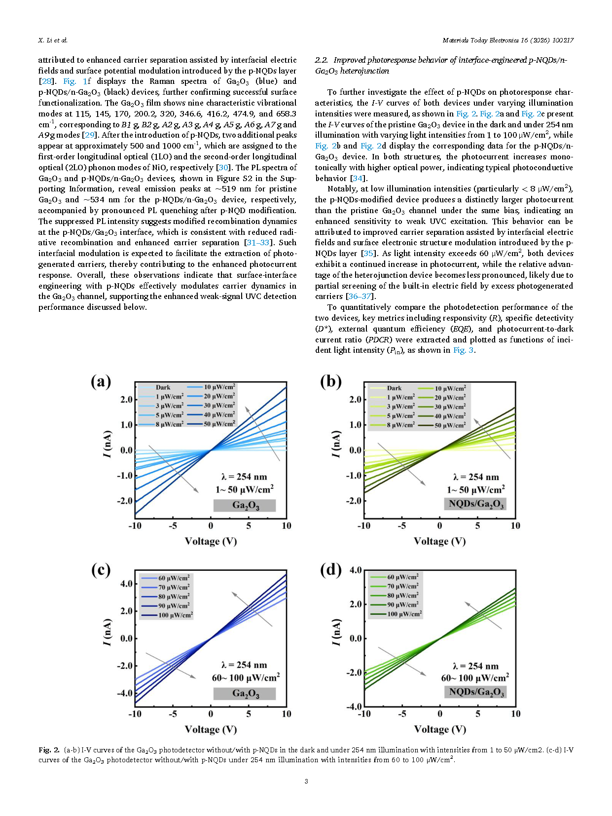
Fig. 3 (a) R, (b) D*, (c) EQE, (d) PDCR of the Ga₂O₃ and the p-NQDs/n-Ga₂O₃ photodetectors as a function of Pin. Insets highlight differences in the low-intensity regime.
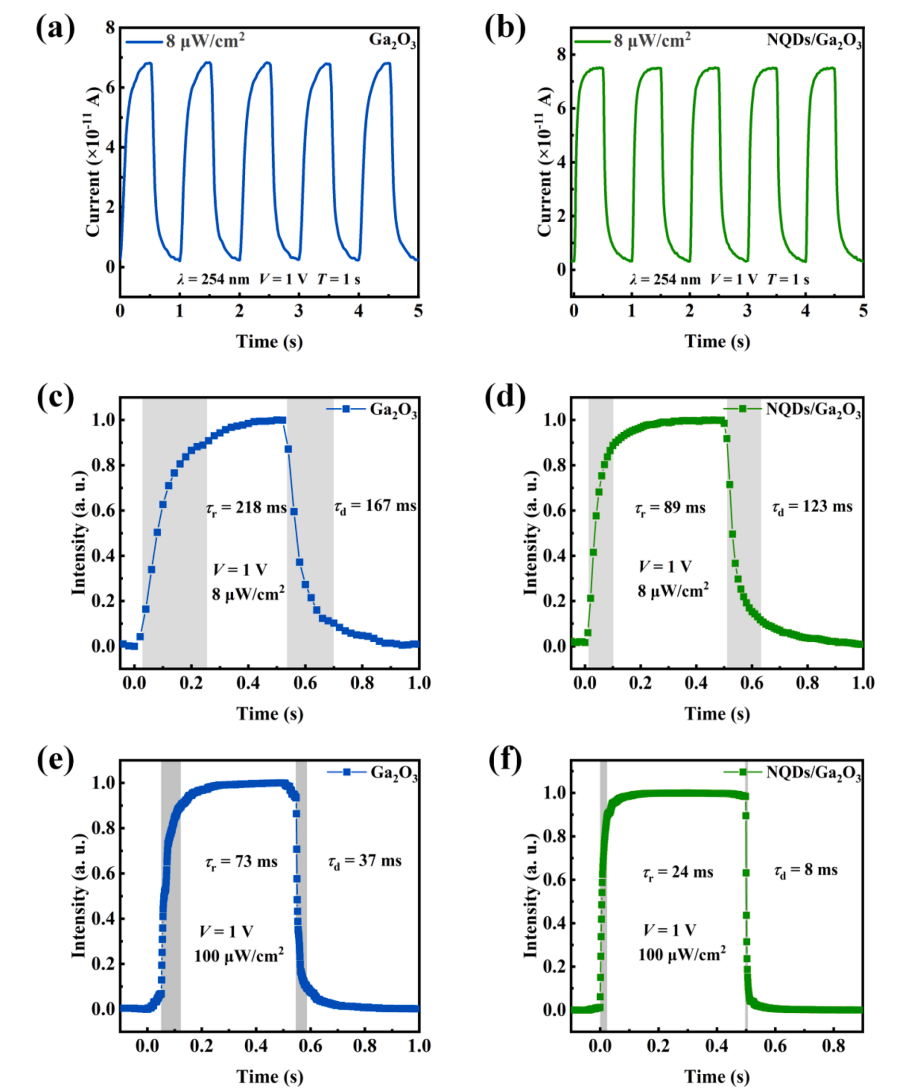
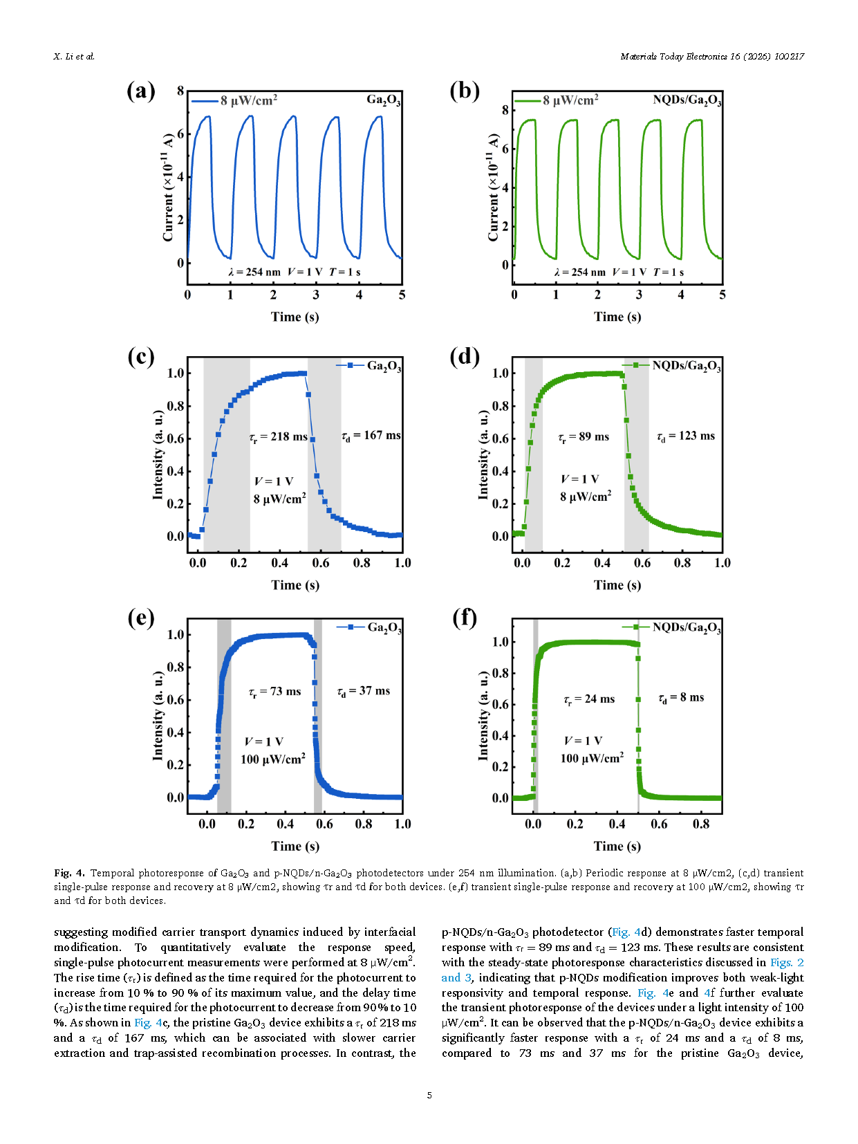
Fig. 4 Temporal photoresponse of Ga₂O₃ and p-NQDs/n-Ga₂O₃ photodetectors under 254 nm illumination. (a,b) Periodic response at 8 µW/cm², (c,d) transient single-pulse response and recovery at 8 µW/cm², showing tr and td for both devices. (e,f) transient single-pulse response and recovery at 100 µW/cm², showing tr and td for both devices.
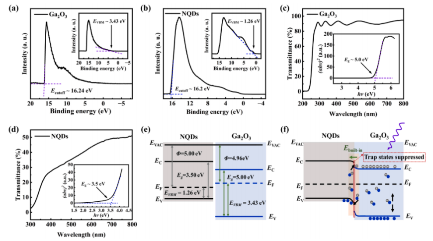
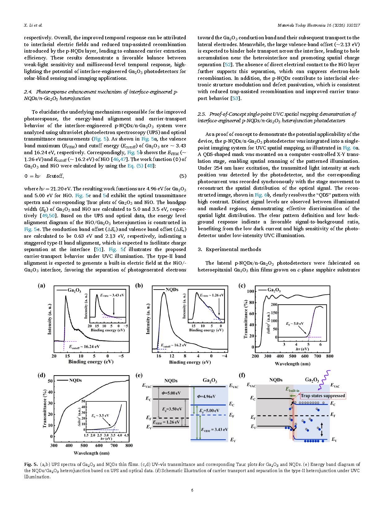
Fig. 5 (a,b) UPS spectra of Ga₂O₃ and NQDs thin films. (c,d) UV-vis transmittance and corresponding Tauc plots for Ga₂O₃ and NQDs. (e) Energy band diagram of the NQDs/Ga₂O₃ heterojunction based on UPS and optical data. (f) Schematic illustration of carrier transport and separation in the type-II heterojunction under UVC illumination.
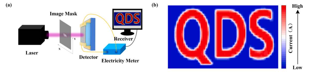
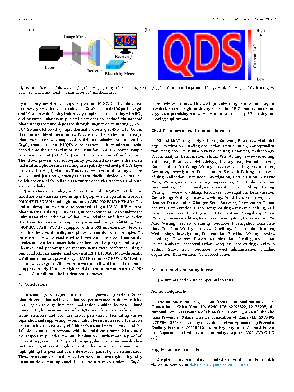
Fig. 6 (a) Schematic of the UVC single-point imaging setup using the p-NQDs/n-Ga₂O₃ photodetector and a patterned image mask. (b) Images of the letter “QDS” obtained with single-point imaging under 254 nm illumination
DOI :
10.1016/j.mtelec.2026.100217.