Paper Sharing
【Member Papers】Insight Into the Performance Degradation of p-NiO/n-Ga₂O₃ Heterojunction Barrier Schottky Diode Under Forward Bias Stress
日期:2026-04-03阅读:28
Researchers from the College of Integrated Circuit Science and Engineering, Nanjing University of Posts and Telecommunications, School of Integrated Circuits and State Key Laboratory of Information Photonics and Optical Communications, Beijing University of Posts and Telecommunications, School of Electronic Information Engineering, Inner Mongolia University have published a dissertation titled "Insight Into the Performance Degradation of p-NiO/n-Ga₂O₃ Heterojunction Barrier Schottky Diode Under Forward Bias Stress" in IEEE TRANSACTIONS ON ELECTRON DEVICES.
Background
β-Ga₂O₃ shows great application potential in high-voltage and high-power electronic devices due to its ~4.9 eV ultrawide bandgap, 8 MV/cm ultrahigh electric field strength and BFOM far exceeding silicon. The melt-based technology for its substrate fabrication is low-cost, with commercial large-size conductive substrates and mature n-type doped epitaxy technology, making it a promising candidate for next-generation power semiconductors. However, the lack of p-type Ga₂O₃ severely restricts the development of bipolar devices, so unipolar Ga₂O₃ SBD is expected to be the first Ga₂O₃-based device applied in power electronic systems. As a p-type semiconductor, NiO has a bandgap of 3.4–4 eV and a critical electric field of 2–5 MV/cm. The p-NiO/n-Ga₂O₃ HJBS constructed by NiO achieves kilovolt-level performance, performs excellently in high-current applications, and its static performance is comparable to commercial power devices. Existing studies mostly focus on the accumulation of interface states of SBD under forward bias stress, while HJBS needs to consider both Schottky contact and NiO/Ga₂O₃ heterointerface states, and the understanding of its interface properties and degradation mechanisms is insufficient. Therefore, the team carried out research on the degradation and recovery behaviors of HJBS under forward bias stress at different temperatures.
Abstract
In this work, we systematically investigated the degradation and recovery behaviors of p-NiO/n-Ga₂O₃ heterojunction barrier Schottky diodes (HJBS) under high-temperature forward bias (HTFB) stress. Furthermore, based on the observed degradation trends in the device’s DC characteristics, a comprehensive analysis was conducted to elucidate the underlying degradation mechanisms. The as-fabricated HJBS structure, based on a p-NiO/n-Ga₂O₃ heterojunction, exhibited excellent electrical performance with a breakdown voltage exceeding 1 kV and an on-resistance of 9.23 mΩ·cm². However, during actual circuit operation, devices are inevitably subjected to high-temperature and high-current stress conditions, leading to significant degradation in turn-on voltage and on-resistance. These challenges impose stricter requirements on the reliability of HJBS devices. The device underwent forward bias stress followed by recovery evaluation. After the forward bias stress (2.5 V at 25 ◦C) for 15 ks, only a 5.2% degradation in the turn-on voltage increase (ΔVₒₙ) was observed. This degradation is attributed to the electron capture associated with donor traps. During the subsequent recovery phase, a nonrecoverable degradation of 2.7% in ΔVₒₙ was recorded, which is believed to be caused by the presence of defects compensation or passivation within the bulk material that impeded the release of trapped electrons. These findings provide important insights for improving the reliability of Ga₂O₃ power devices.
Highlights
Innovative testing method:For the first time, the MSM (Measurement-Stress-Measurement) method was adopted to study the degradation and recovery behaviors of key electrical parameters of β-Ga₂O₃-based HJBS devices under forward bias stress at different temperatures.
Device performance characterization:The fabricated p-NiO/n-Ga₂O₃ HJBS device has a breakdown voltage of 1035 V, which is 2.65 times that of the traditional Ga₂O₃ SBD device, with a low on-resistance of 9.23 mΩ·cm², smaller leakage current and better switching performance.
Revelation of degradation rules:The influence laws of temperature and stress voltage on the turn-on voltage degradation of HJBS and SBD devices were clarified. High temperature and high stress voltage will aggravate the non-recoverable degradation of devices, and the degradation degree of HJBS is lower than that of SBD as a whole.
Combination of characterization methods:Combined with J-V (current-voltage), C-f (capacitance-frequency) and C-V (capacitance-voltage) tests and characterizations, the microscopic processes of device degradation and recovery were analyzed from the perspective of changes in electrical characteristics.
In-depth mechanism explanation:It is clarified that the degradation of HJBS devices under forward bias stress is caused by internal thermal load and electron trapping at defects, and the non-recoverable degradation is caused by stable defect compensation/passivation mechanisms in the bulk material.
Clear application value:The reliability mechanism of Ga₂O₃ heterojunction is revealed, which provides theoretical guidance for material optimization, defect control and long-term stability improvement of ultra-wide bandgap power electronic devices.
Conclusion
In conclusion, this work systematically investigates the performance degradation and recovery mechanisms of p-NiO/n-Ga₂O₃ HJBS under forward stress through the application of the MSM technique. The observed increase in Vₒₙ under forward bias stress is primarily attributed to internal thermal load and electron trapping at defect sites. Notably, the identification of a nonrecoverable degradation component indicates the involvement of stable defect compensation or passivation mechanisms within the bulk material, which permanently hinder the complete release of trapped charge carriers. Current and capacitance characterization (C-f, J-V) indicate that the degradation and recovery under forward bias stress are caused by the dynamic equilibrium of acceptor-like interface traps capture and emission processes, which are further involved in TAT processes and subsequently captured by bulk traps. These insights elucidate the reliability mechanisms of Ga₂O₃ heterojunctions, thereby guiding material and defect optimization to enhance the long-term stability of ultra-wide bandgap power electronics.
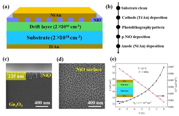
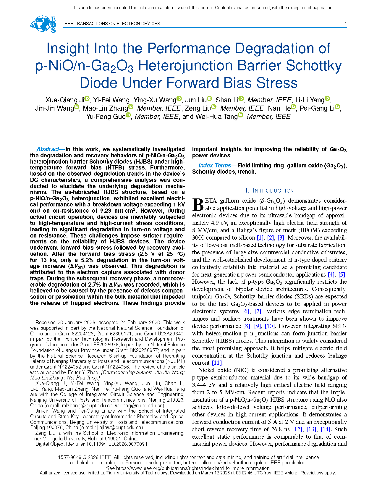
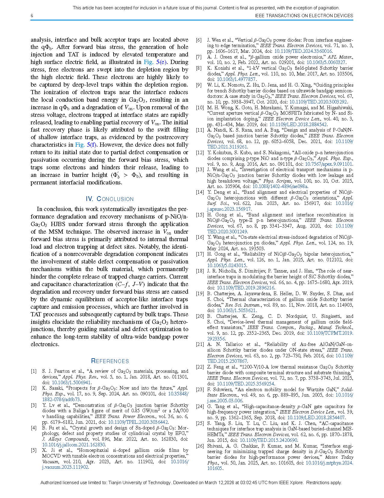
Fig. 1. (a) Schematic diagram of the HJBS structure. (b) Key process flows involved in the fabrication of the HJBS. (c) Corresponding cross-sectional SEM images of the Ga₂O₃/NiO heterojunction. (d) SEM images of the NiO surface. (e) C–V and C⁻²-V plots for the Ga₂O₃ SBD devices.
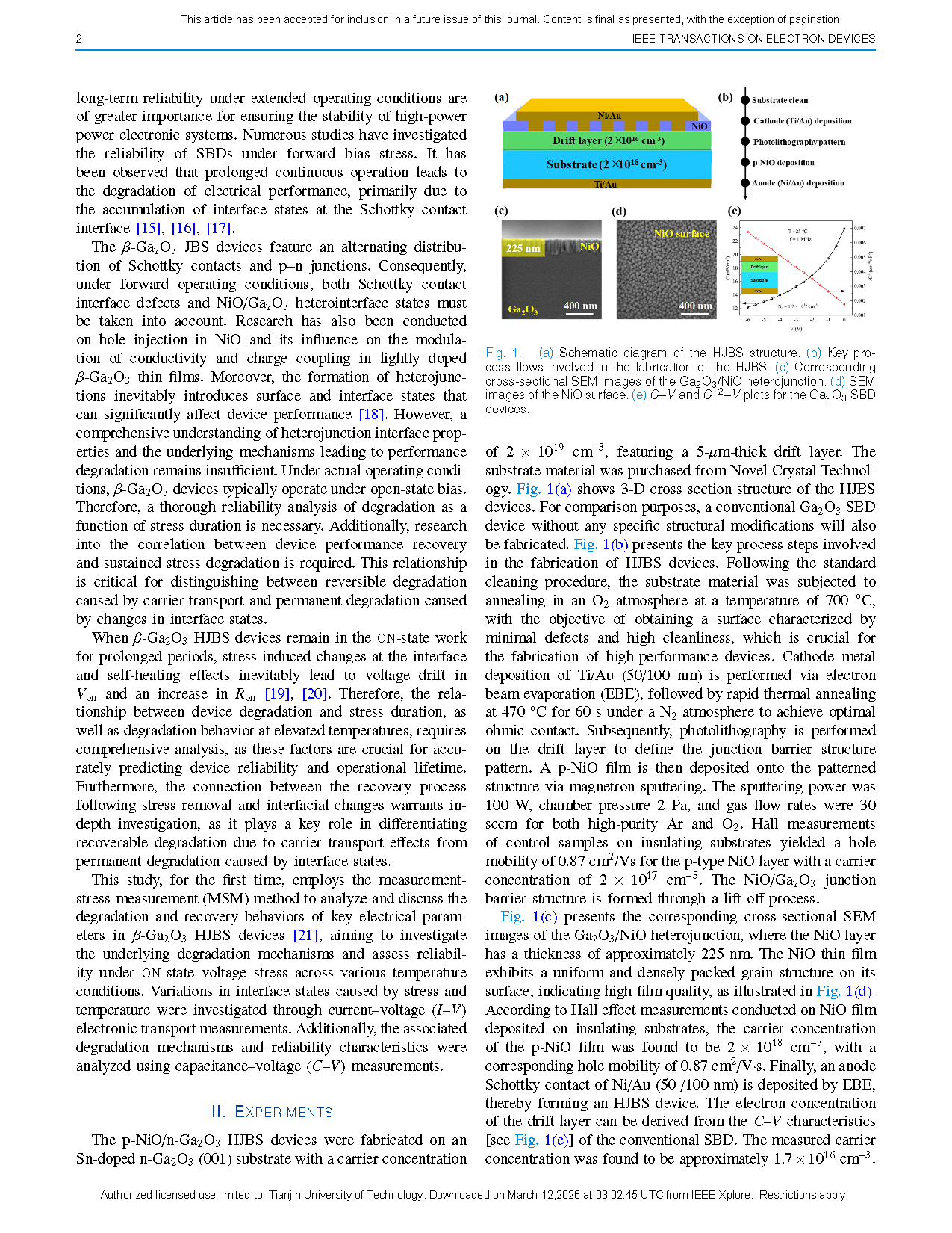
Fig. 2. (a) The forward current density–voltage characteristics and Rₒₙ versus forward bias, (b) semi-logarithmic plot illustrating the forward current–voltage, and (c) breakdown characteristics of the two different structures with simulation diagram of electric field distribution.
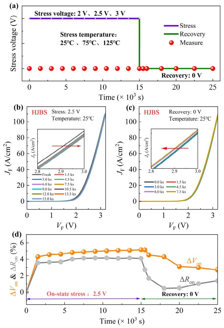
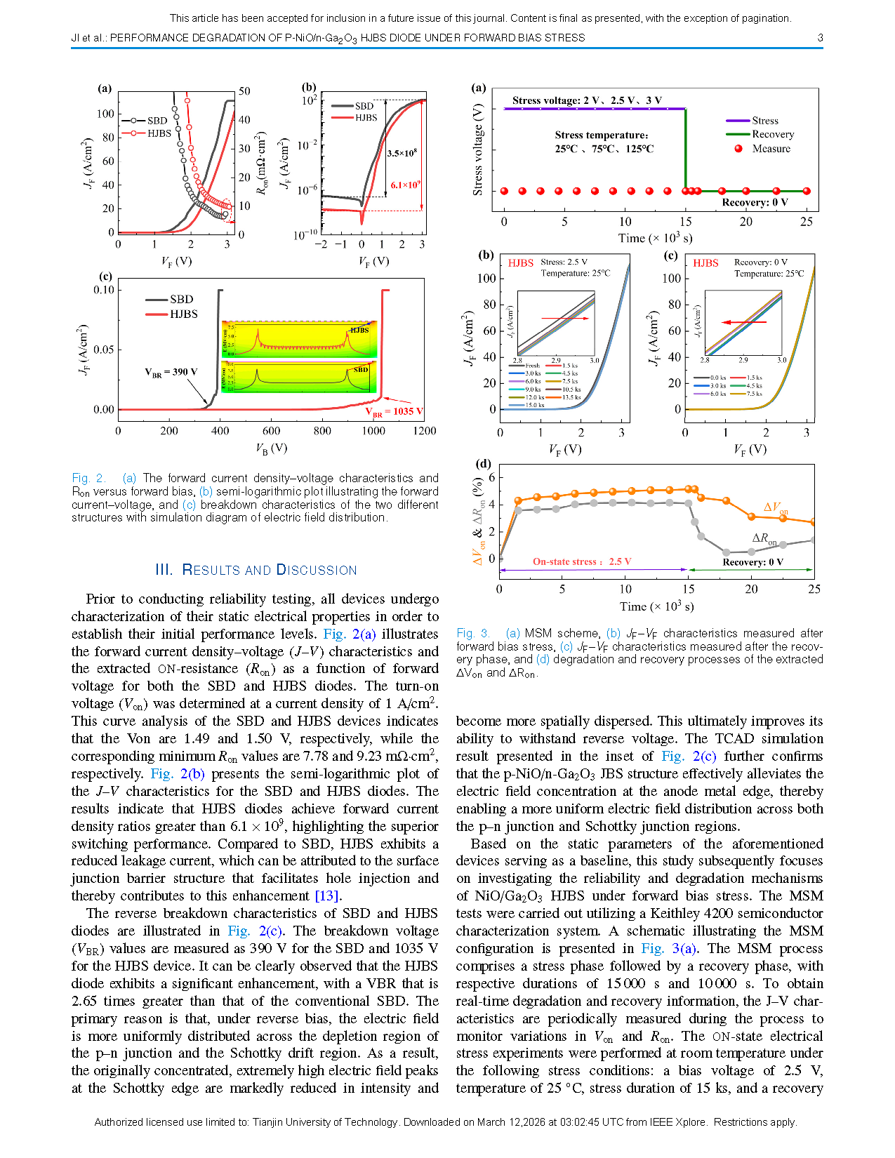
Fig. 3. (a) MSM scheme, (b) JF-VF characteristics measured after forward bias stress, (c) JF-VF characteristics measured after the recovery phase, and (d) degradation and recovery processes of the extracted ΔVₒₙ and ΔRₒₙ.
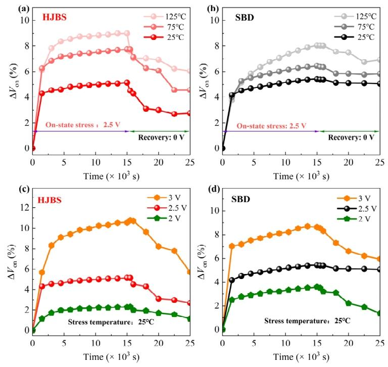
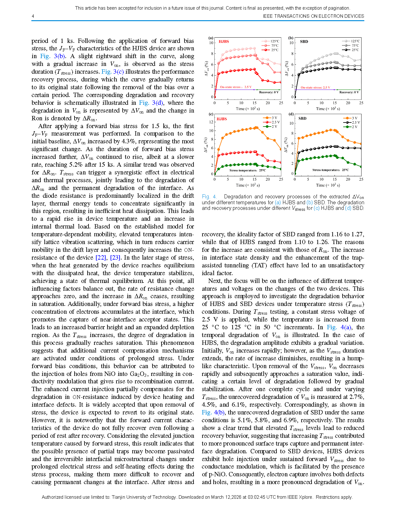
Fig. 4. Degradation and recovery processes of the extracted ΔVₒₙ under different temperatures for (a) HJBS and (b) SBD. The degradation and recovery processes under different Vₛₜᵣₑₛₛ for (c) HJBS and (d) SBD.
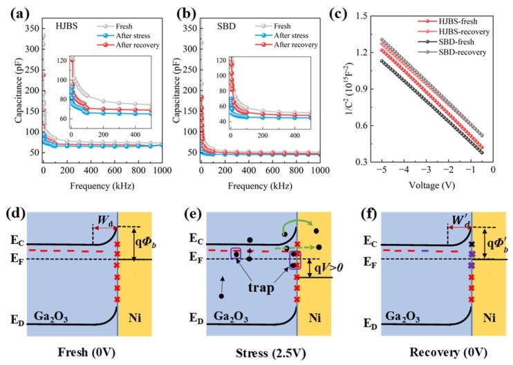
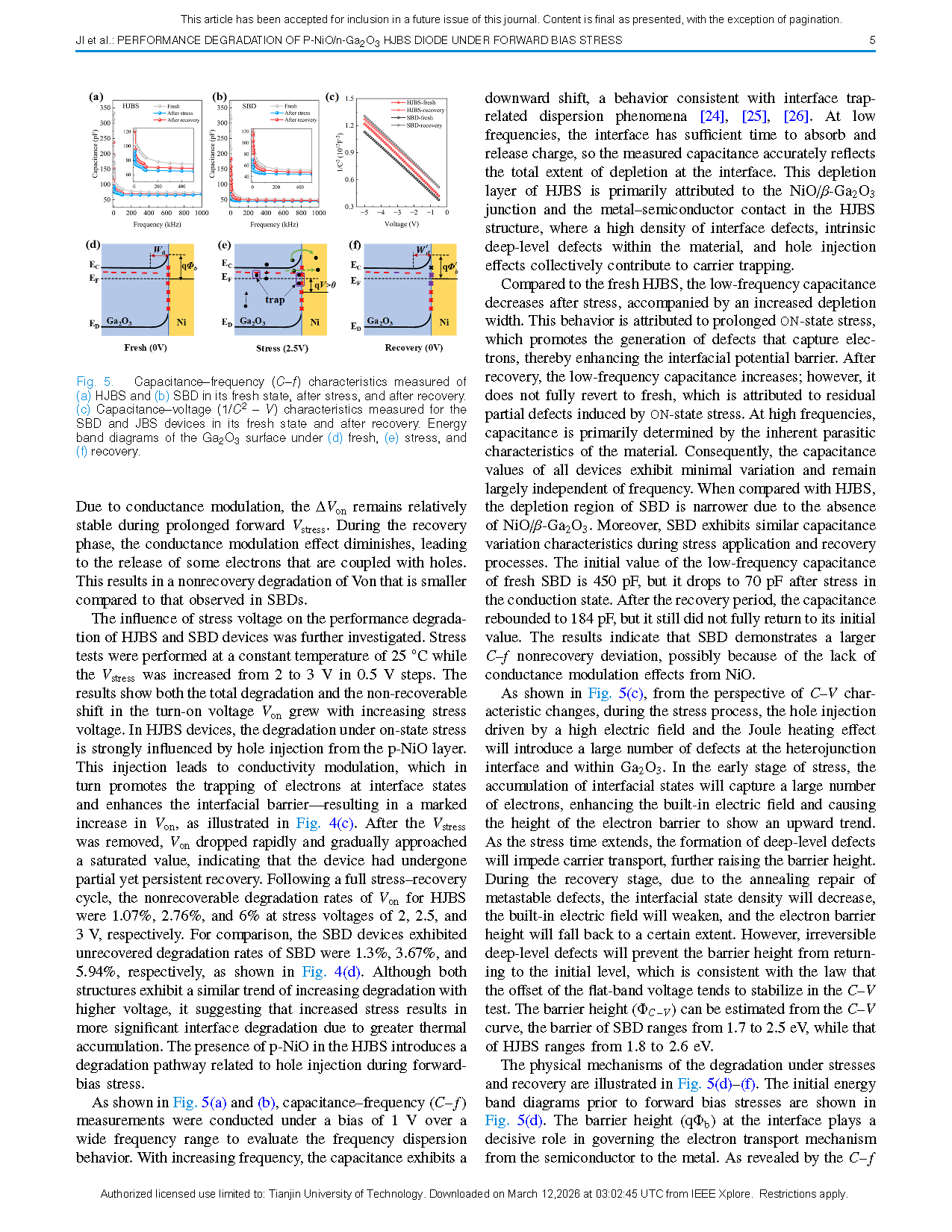
Fig. 5. Capacitance–frequency(C–f ) characteristics measured of (a) HJBS and (b) SBD in its fresh state, after stress, and after recovery. (c) Capacitance–voltage (1 / C²-V) characteristics measured for the SBD and JBS devices in its fresh state and after recovery. Energy band diagrams of the Ga₂O₃ surface under (d) fresh, (e) stress, and (f) recovery.
DOI:
10.1109/TED.2026.3670091