Paper Sharing
【Member Papers】Electro-thermal crosstalk revealed by Raman thermography in multi-fin β-Ga₂O₃ FinFETs
日期:2026-04-02阅读:195
Researchers from the Xi’an Jiaotong University and Xidian University have published a dissertation titled " Electro-thermal crosstalk revealed by Raman thermography in multi-fin β-Ga2O3 FinFETs" in Applied Physics Letters.
Background
β-Ga2O3 has emerged as a highly promising material for next generation high-power electronic applications owing to its superior intrinsic properties. These include a wide direct bandgap of 4.8 eV (Eg), an exceptionally high critical electric field of 8 MV/cm, a moderate carrier mobility of 250−300 cm2/Vs , a high electron saturation velocity of 1.8−2×107 cm/s , and a high theoretical Baliga’s figure of merit (BFOM). While absolute values vary depending on critical electric field estimates,3 it is widely projected to be approximately 3444 times that of Si. Furthermore, the growth technology of β-Ga2O3 is relatively well developed, allowing for controllable n-type doping across a wide concentration range (1016-1019 cm-3). The availability of high-quality, low-cost bulk substrates produced via melt growth methods also provides unique opportunities for the fabrication of cost-effective, high-performance transistors. This advantage directly addresses the high manufacturing costs associated with SiC and GaN, thereby paving the way for the advancement of device technologies 8–10 and their potential large-scale commercialization.
Abstract
β-Ga2O3 FinFETs are promising for high-power electronic applications owing to their ultra-wide bandgap and high breakdown field. To overcome the inherently limited current capability of single-fin devices, multi-fin architectures were introduced to enhance the total on-state current. However, transfer characteristics reveal that when the fin number is increased by a factor of 16, the saturation current at VD =10 V rises only from 0.112 to 1.22 mA—significantly below the expected linear scaling—and premature current degradation emerges at high VG Such deviation indicates pronounced self-heating and electro-thermal coupling within densely packed fin arrays. Furthermore, under high power operation, evident nonlinearities appear in both temperature rise and current response, further supporting the thermally driven origin of performance degradation. Raman thermography under identical per-fin current conditions reveals a much higher peak temperature (70.77 °C) in the multi-fin device compared to the single-fin counterpart (28.8 °C), confirming severe thermal crosstalk. These findings elucidate the thermal origin of the non-ideal current scalability and provide essential insights for thermally aware three-dimensional design of β-Ga2O3 FinFETs.
Highlights
Combining submicron-resolution Raman thermography with electrical measurements, the study achieves accurate spatial temperature characterization of β-Ga2O3 multi-fin/single-fin FinFETs under the condition of equal power per fin, and also calibrates and selects a highly sensitive Raman temperature measurement mode while considering the influence of stress on temperature measurement, thus improving the accuracy of thermal characterization.
An electro-thermal compact model adapted to β-Ga2O3 is constructed, the current scaling efficiency φ(N) is defined for the first time and the effective mobility-temperature exponent meff≈14 is extracted, realizing the quantitative evaluation of thermally induced current degradation and non-ideal current scaling of such devices.
The study systematically reveals that thermal crosstalk caused by the low and anisotropic thermal conductivity and the geometric constraints of high-density fin arrays is the core thermal cause of non-ideal current scaling in β-Ga2O3 multi-fin FinFETs, and proposes the device design optimization directions of moderately reducing the number of fins and optimizing the three-dimensional layout.
Conclusion
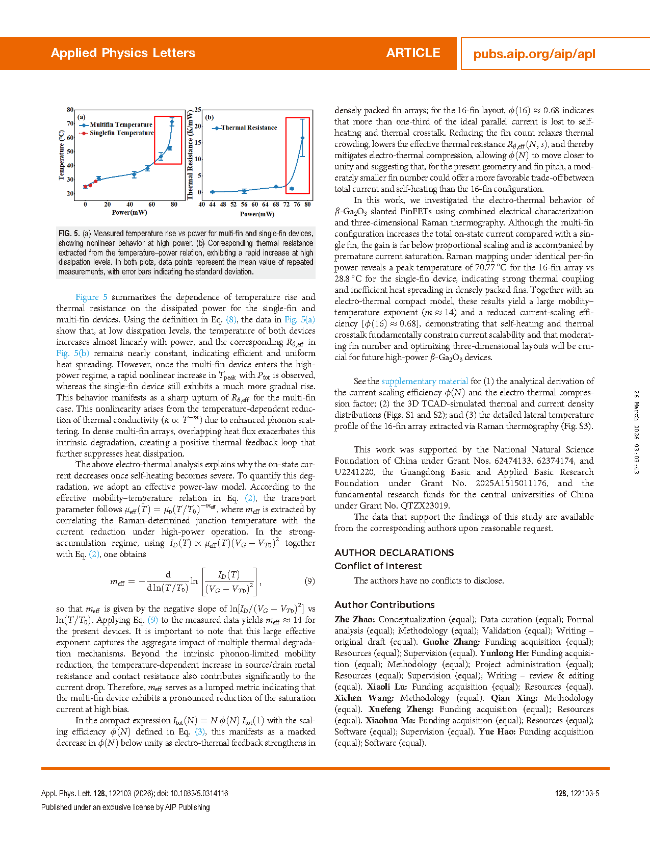
In this work, we investigated the electro-thermal behavior of β-Ga2O3 slanted FinFETs using combined electrical characterization and three-dimensional Raman thermography. Although the multi-fin configuration increases the total on-state current compared with a single fin, the gain is far below proportional scaling and is accompanied by premature current saturation. Raman mapping under identical per-fin power reveals a peak temperature of 70.77 °C for the 16-fin array vs 28.8 °C for the single-fin device, indicating strong thermal coupling and inefficient heat spreading in densely packed fins. Together with an electro-thermal compact model, these results yield a large mobility– temperature exponent ( m≈14 ) and a reduced current-scaling efficiency [φ(16)≈0.68] , demonstrating that self-heating and thermal crosstalk fundamentally constrain current scalability and that moderating fin number and optimizing three-dimensional layouts will be crucial for future high-power β-Ga2O3 devices.
Project Support
This work was supported by the National Natural Science Foundation of China under Grant Nos. 62474133, 62374174, and U2241220, the Guangdong Basic and Applied Basic Research Foundation under Grant No. 2025A1515011176, and the fundamental research funds for the central universities of China under Grant No. QTZX23019.
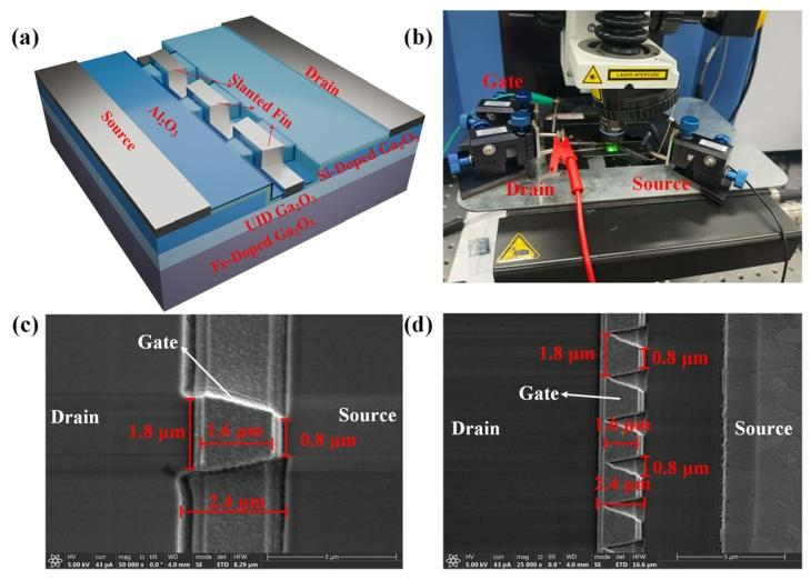
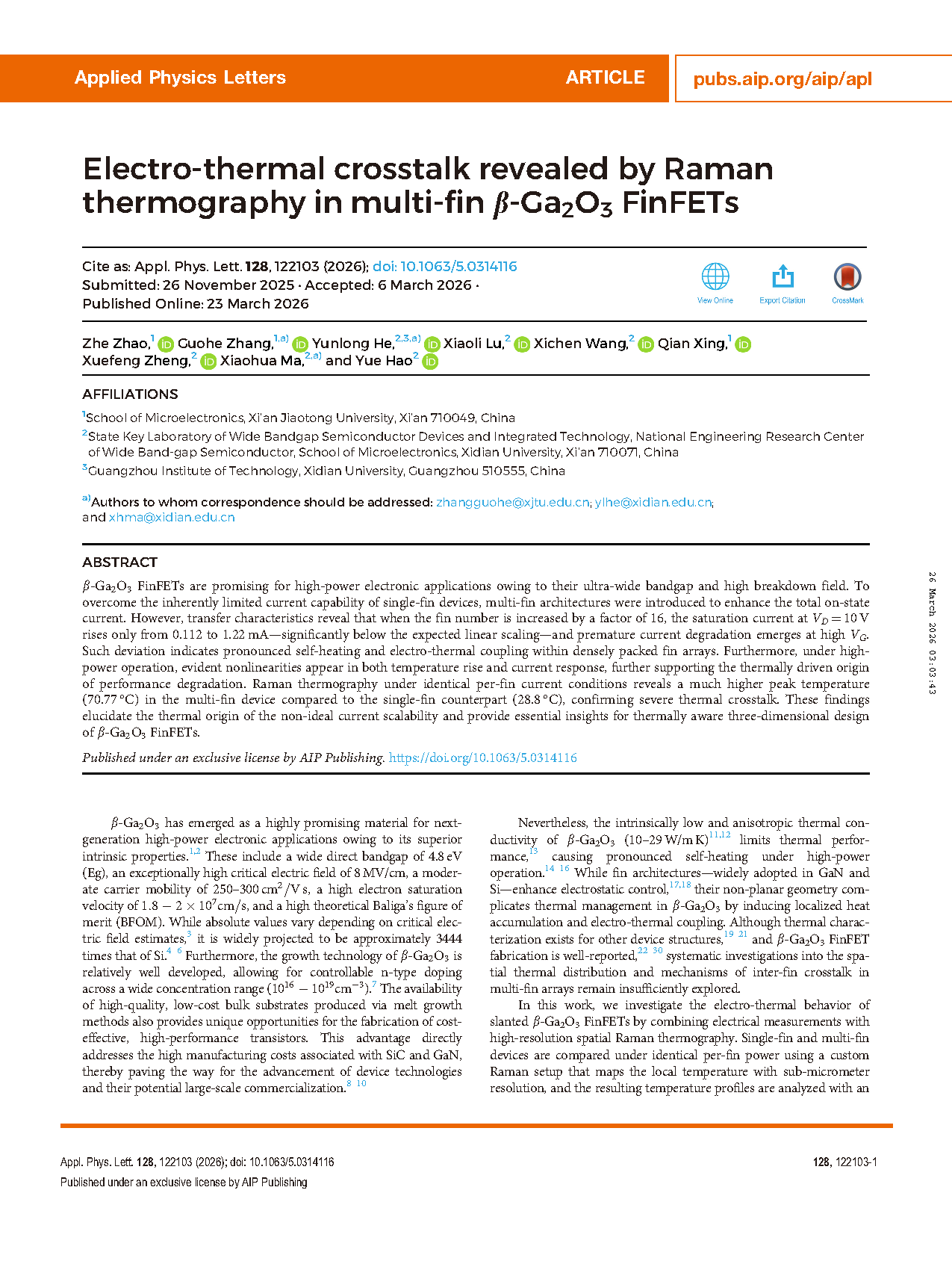
Fig. 1 (a) Three-dimensional schematic of the slanted-fin device. (b) Photograph of the experimental layout. (c) SEM image of a single-fin device. (d) SEM image of a multi-fin device with fin array configuration.
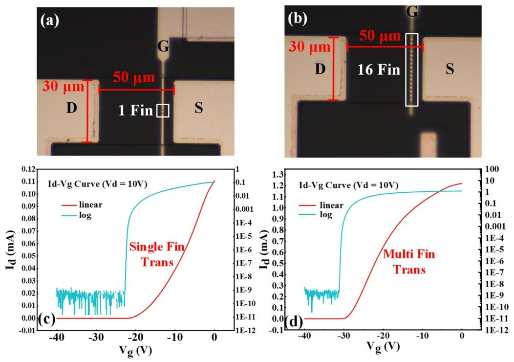
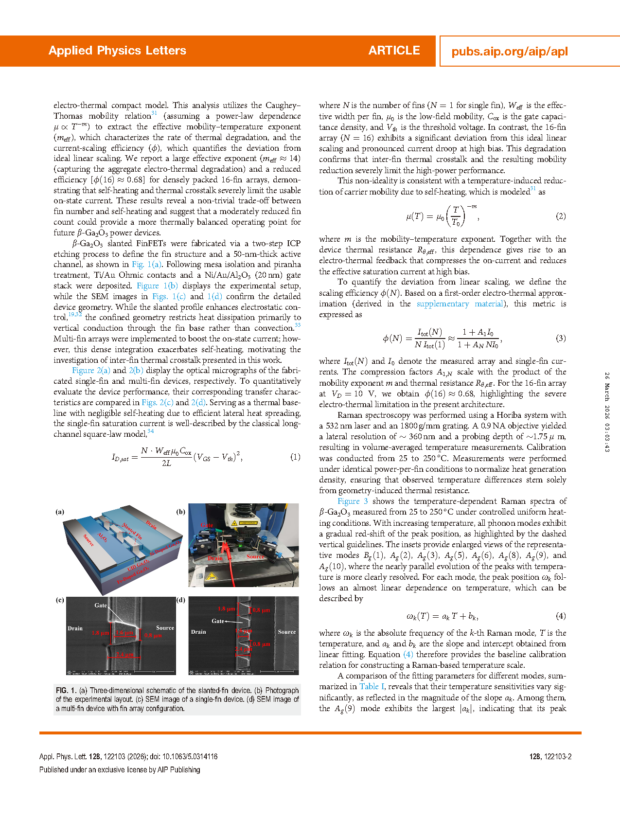
Figure 2. (a) Optical micrograph of the fabricated single-fin β-Ga2O3 FinFET.(b) Optical micrograph of the fabricated multi-fin β-Ga2O3 FinFET. (c) Transfer characteristics of the single-fin device. (d) Transfer characteristics of the multi-fin device.
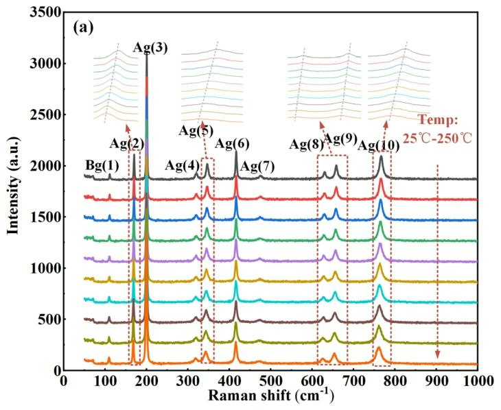
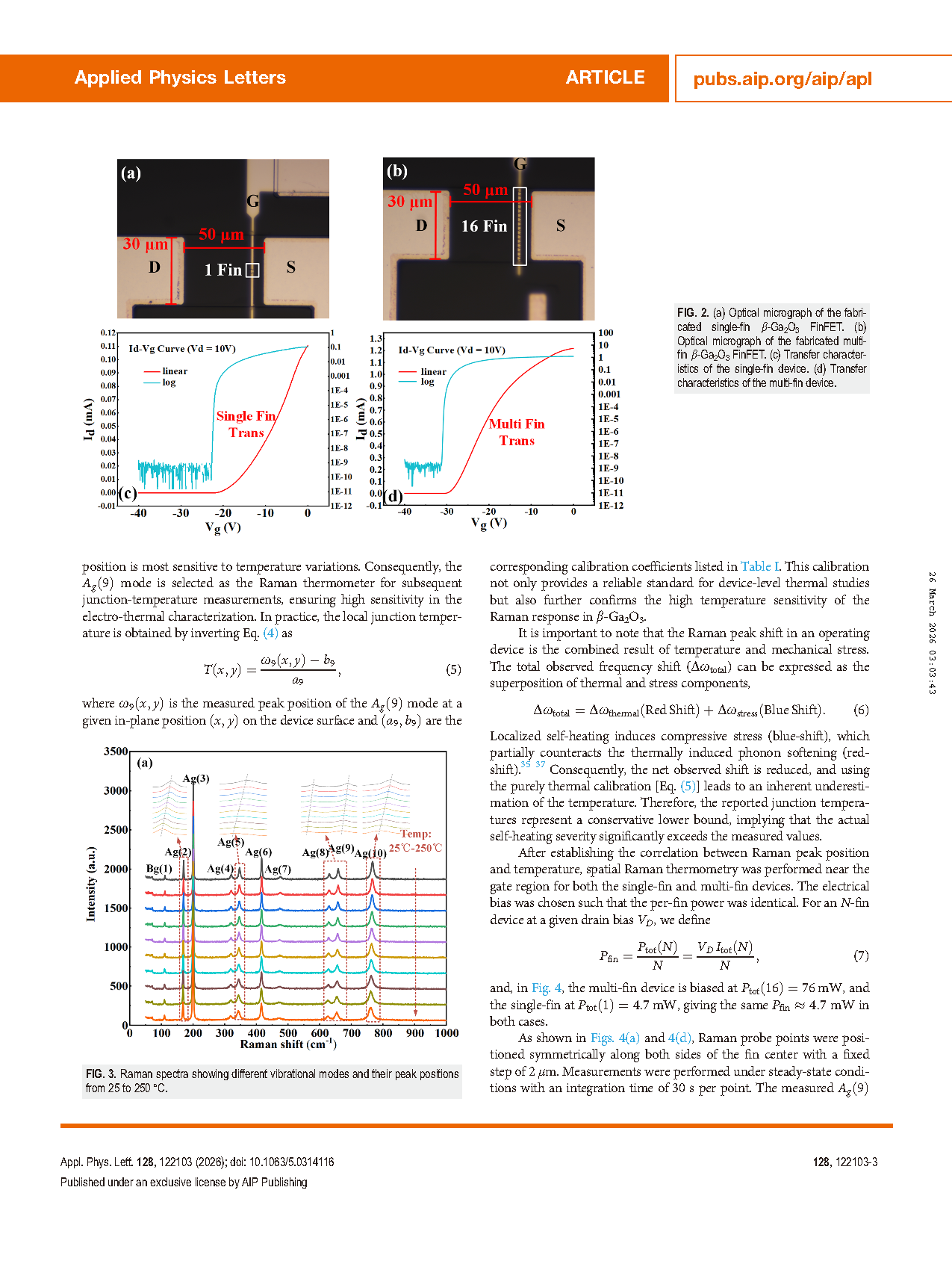
Figure 3. Raman spectra showing different vibrational modes and their peak positions from 25 to 250 °C.

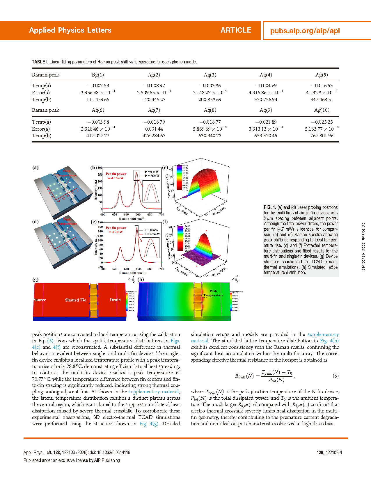
Figure 4. (a) and (d) Laser probing positions for the multi-fin and single-fin devices with 2 μm spacing between adjacent points. (b) and (e) Raman spectra showing peak shifts corresponding to local temperature rise. (c) and (f) Extracted temperature distributions and fitted results for the multi-fin and single-fin devices. (g) Device structure constructed for TCAD electro-thermal simulations. (h) Simulated lattice temperature distribution.
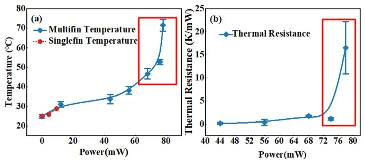
Figure 5. (a) Measured temperature rise vs power for multi-fin and single-fin devices, showing nonlinear behavior at high power. (b) Corresponding thermal resistance extracted from the temperature–power relation, exhibiting a rapid increase at high dissipation levels. In both plots, data points represent the mean value of repeated measurements, with error bars indicating the standard deviation.
DOI:
doi.org/10.1063/5.0314116