Paper Sharing
【Member Papers】Synergistic work function modulation and interface traps suppression in CuCrO₂/β-Ga₂O₃ p-n heterojunction diodes through oxygen vacancy passivation
日期:2026-03-30阅读:169
A research team led by Prof. Weifeng Yang from Xiamen University has published a paper in the international journal Journal of Alloys and Compounds, entitled:Synergistic work function modulation and interface traps suppression in CuCrO₂/β-Ga₂O₃ p-n heterojunction diodes through oxygen vacancy passivation.
Background
Gallium oxide (Ga₂O₃), as an emerging ultra-wide bandgap semiconductor, features a wide bandgap of 4.9 eV and a high critical breakdown field of 8 MV/cm, showing great potential for next-generation high-power electronic devices. In addition, it supports melt growth of large-size wafers, offering advantages for low-cost industrial-scale production. However, due to the strong localization of holes, achieving effective p-type doping remains a key bottleneck. To overcome this limitation, integrating p-type materials such as Cu₂O, SnO, and NiO with n-type β-Ga₂O₃ to form heterojunction diodes (HJDs) has become a mainstream strategy. Among them, delafossite-structured CuCrO₂ is considered a highly promising p-type transparent oxide due to its high transparency, excellent thermal stability, and tunable carrier concentration. However, CuCrO₂ films prepared by magnetron sputtering typically contain a high density of intrinsic defects, especially oxygen vacancies (VO). These oxygen vacancies act as donor states, compensating acceptors and suppressing p-type conductivity. In addition, VO-related traps in both the bulk and interface capture carriers, enhance recombination, and increase leakage current, thereby degrading device performance. Currently, the trap-limited transport mechanisms in CuCrO₂/β-Ga₂O₃ heterojunctions remain insufficiently understood. Therefore, developing effective interface and bulk optimization strategies is crucial for high-efficiency and high-reliability Ga₂O₃-based power devices.
Abstract
This work reports a vertical p–n heterojunction diode based on CuCrO₂/β-Ga₂O₃, with oxygen plasma treatment used to achieve synergistic control of both interface and bulk properties. Experimental results show that oxygen plasma effectively passivates oxygen vacancies in CuCrO₂ and promotes the oxidation of Cu⁺ to Cu²⁺. With reduced oxygen vacancies and increased hole concentration, the contact resistance of Ni/CuCrO₂ decreases, and the specific on-resistance is reduced from 6.4 mΩ·cm² to 5.2 mΩ·cm². In terms of reverse characteristics, the breakdown voltage increases from 1110 V to 1785 V. KPFM measurements show that the work function increases from 4.99 eV to 5.18 eV, and the built-in potential rises from 2.04 V to 2.16 V. The interface trap density decreases from 7.98×10¹² cm⁻²·eV⁻¹ to 6.02×10¹² cm⁻²·eV⁻¹. Leakage paths associated with SRH recombination and Poole–Frenkel emission are effectively suppressed.
Key Innovations
A synergistic oxygen vacancy passivation strategy enables simultaneous optimization of interface and bulk properties.
Device performance is significantly improved, with PFOM increased by 221%.
The work function and built-in potential are simultaneously enhanced, strengthening the rectification barrier.
Trap-related transport mechanisms are suppressed, reducing leakage current.
Conclusion
This study demonstrates that O₂ plasma-induced oxygen vacancy passivation provides a synergistic approach to simultaneously improve the interface and bulk electronic properties of CuCrO₂/β-Ga₂O₃ heterojunction diodes. The treatment enhances the p-type conductivity of CuCrO₂, increases the work function (Φ) and built-in potential , and improves Ni/CuCrO₂ ohmic contact by increasing hole concentration and reducing contact resistivity , thereby lowering the on-resistance. Band alignment analysis shows that the increased conduction band offset strengthens the barrier against electron injection, effectively suppressing reverse leakage. Meanwhile, trap-related mechanisms are mitigated through passivation, reducing dominant leakage paths associated with PF emission and SRH recombination. TCAD simulations further confirm that the O₂ plasma treatment alleviates electric field crowding near the anode by simultaneously increasing hole concentration and reducing interface trap density (Dit), resulting in a more uniform electric field distribution. These results highlight oxygen vacancy passivation as a practical and scalable strategy for simultaneous interface and bulk optimization, offering strong potential for next-generation wide bandgap oxide power electronic devices.
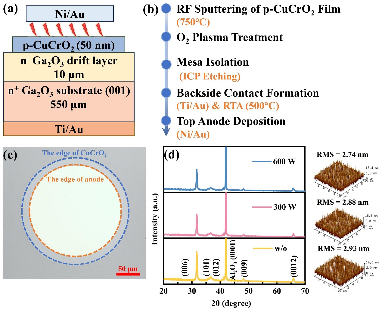
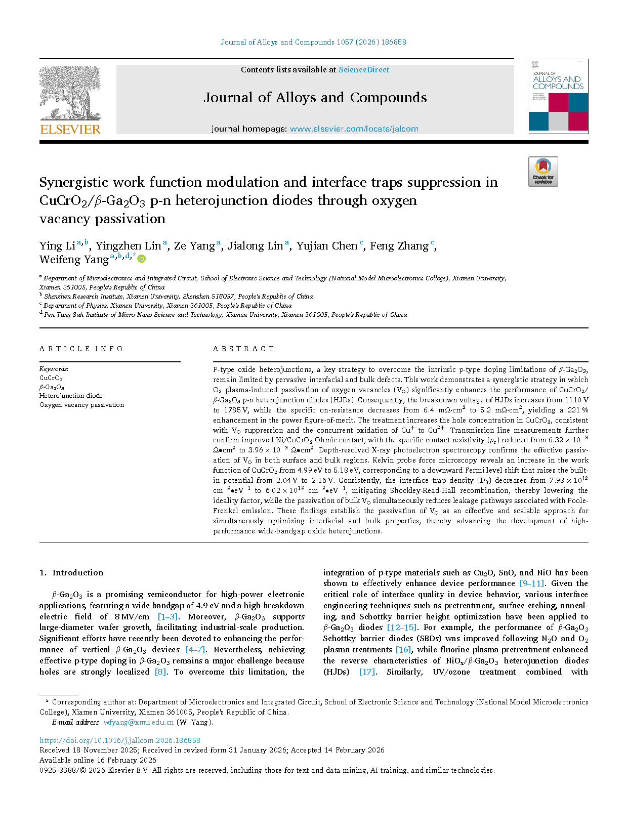
Figure 1.(a) Cross-sectional schematic of the CuCrO₂/β-Ga₂O₃ HJD.(b) Schematic illustration of the key fabrication process.(c) Top-view optical microscope image of the fabricated CuCrO₂/β-Ga₂O₃ HJD.(d) XRD patterns and corresponding AFM surface morphologies of sputtered CuCrO₂ films after O₂ plasma treatment at w/o (0 W), 300 W, and 600 W.
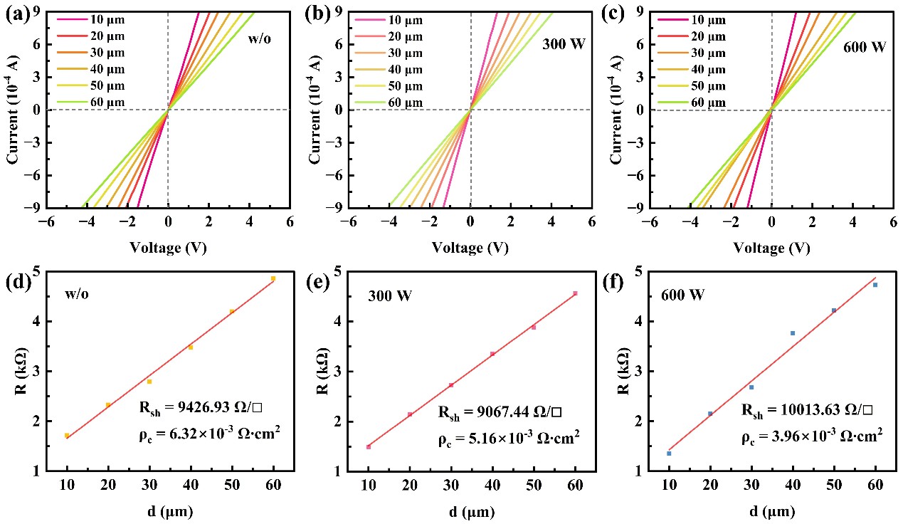
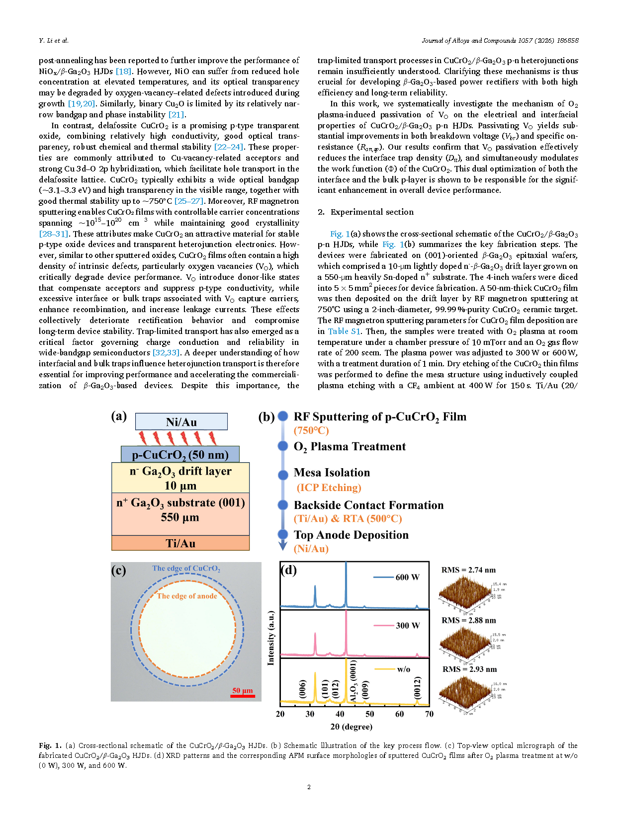
Figure 2. TLM characterization of Ni/CuCrO₂ contacts after O₂ plasma treatment at different powers.(a–c) I–V characteristics measured between adjacent TLM pads with different spacings (d = 10–60 μm) for samples treated at (a) w/o, (b) 300 W, and (c) 600 W.(d–f) Total resistance (R) extracted from the I–V slopes as a function of spacing (d), along with corresponding linear TLM fitting for (d) w/o, (e) 300 W, and (f) 600 W samples.
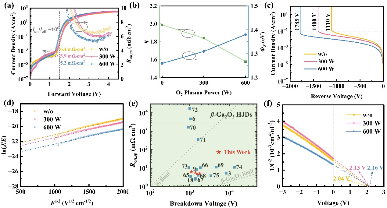
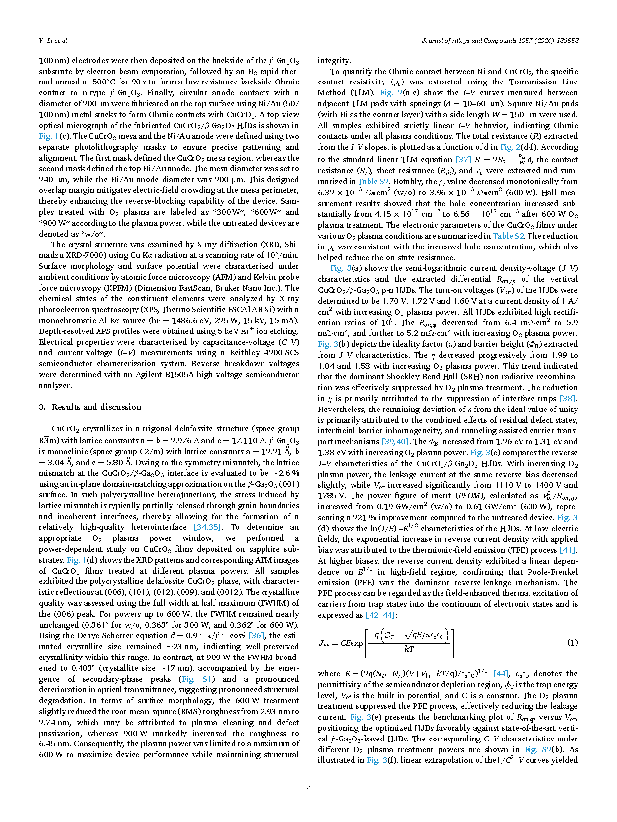
Figure 3.(a) Semi-log forward J–V characteristics and extracted relationship between Ron,sp and forward bias.(b) Variation of ideality factor (η) and barrier height (ΦB).(c) Semi-log reverse J–V characteristics.(d) ln(J/E) versus E¹ᐟ² plots under reverse bias.(e) Benchmark comparison of Ron,sp and breakdown voltage (V_br) for advanced vertical β-Ga₂O₃-based HJDs.(f) 1/C²–V characteristics of CuCrO₂/β-Ga₂O₃ HJDs measured at 1 MHz after O₂ plasma treatment at w/o, 300 W, and 600 W.
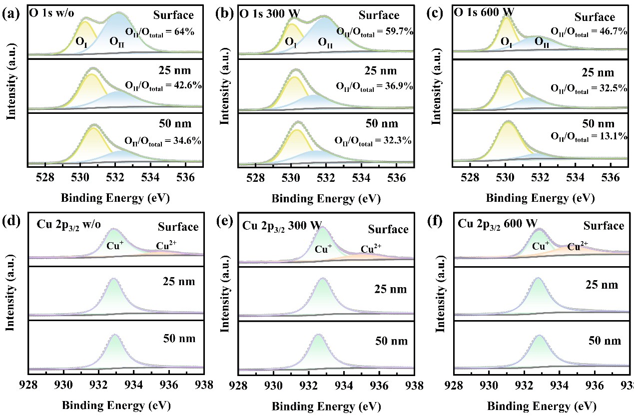
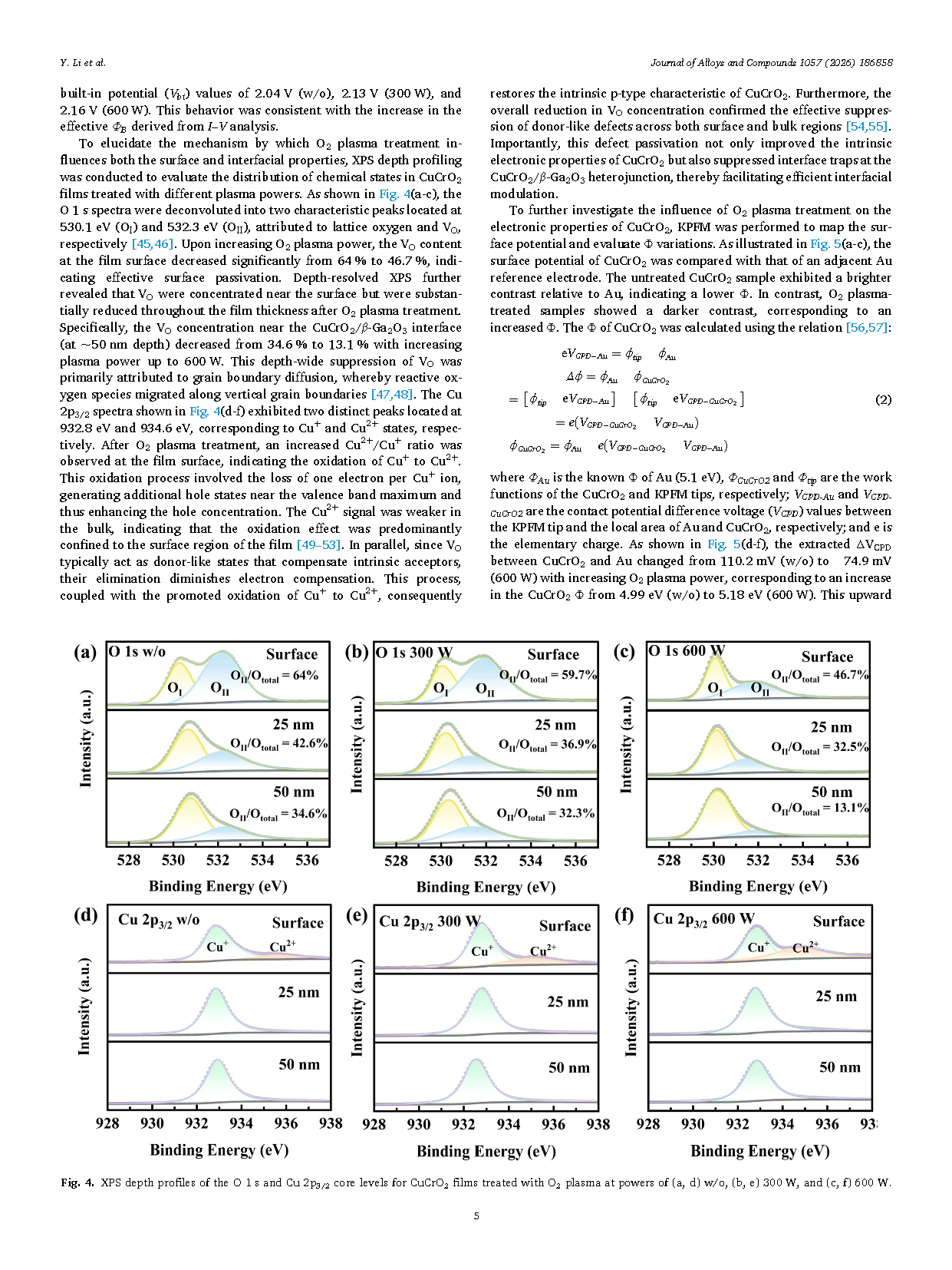
Figure 4. XPS depth profiles of O 1s and Cu 2p₃/₂ core levels in CuCrO₂ films after O₂ plasma treatment at (a, d) w/o, (b, e) 300 W, and (c, f) 600 W.
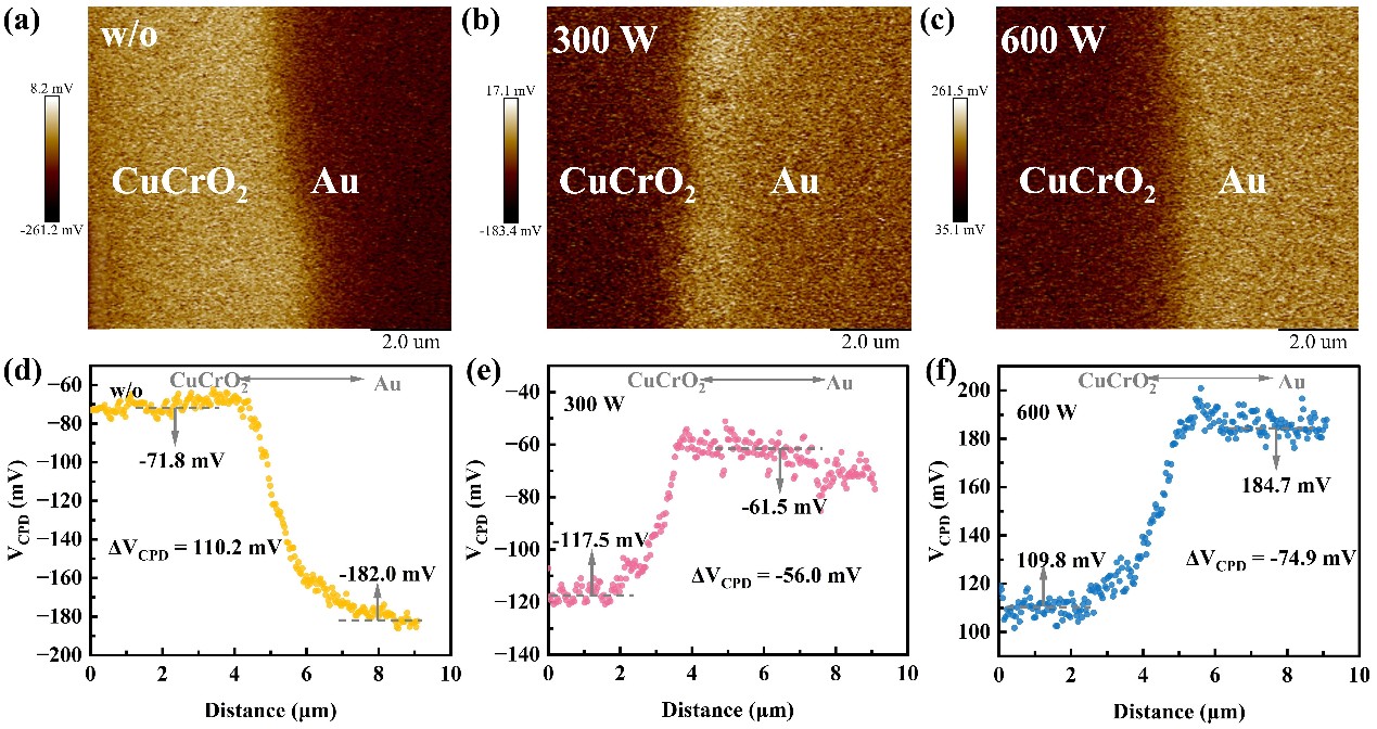
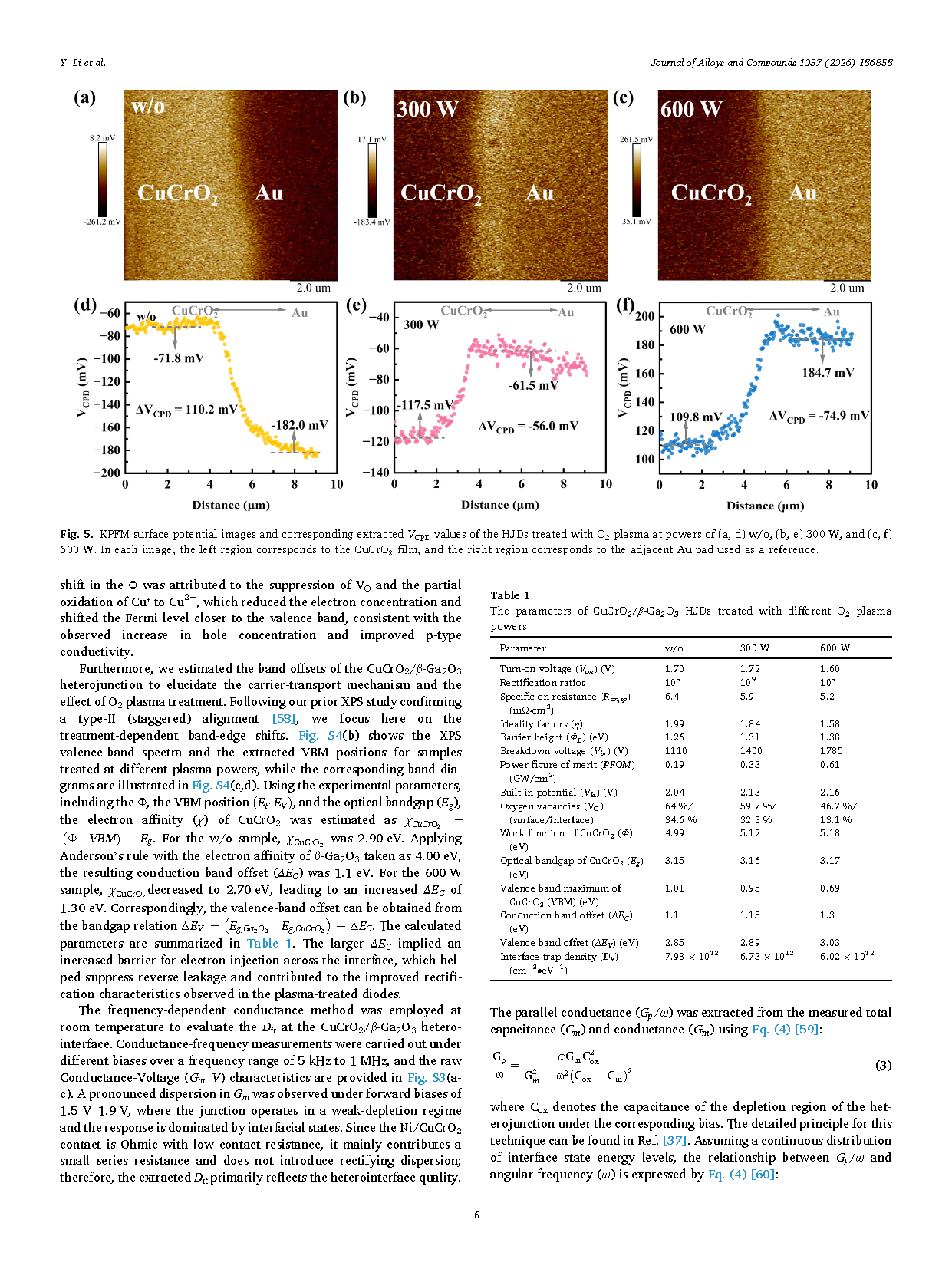
Figure 5. KPFM surface potential images and corresponding extracted contact potential difference (V_CPD) values of HJDs after O₂ plasma treatment at (a, d) w/o, (b, e) 300 W, and (c, f) 600 W. In each image, the left region corresponds to the CuCrO₂ film, while the right region corresponds to the adjacent Au pad used as a reference.
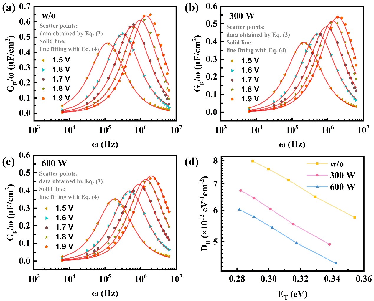
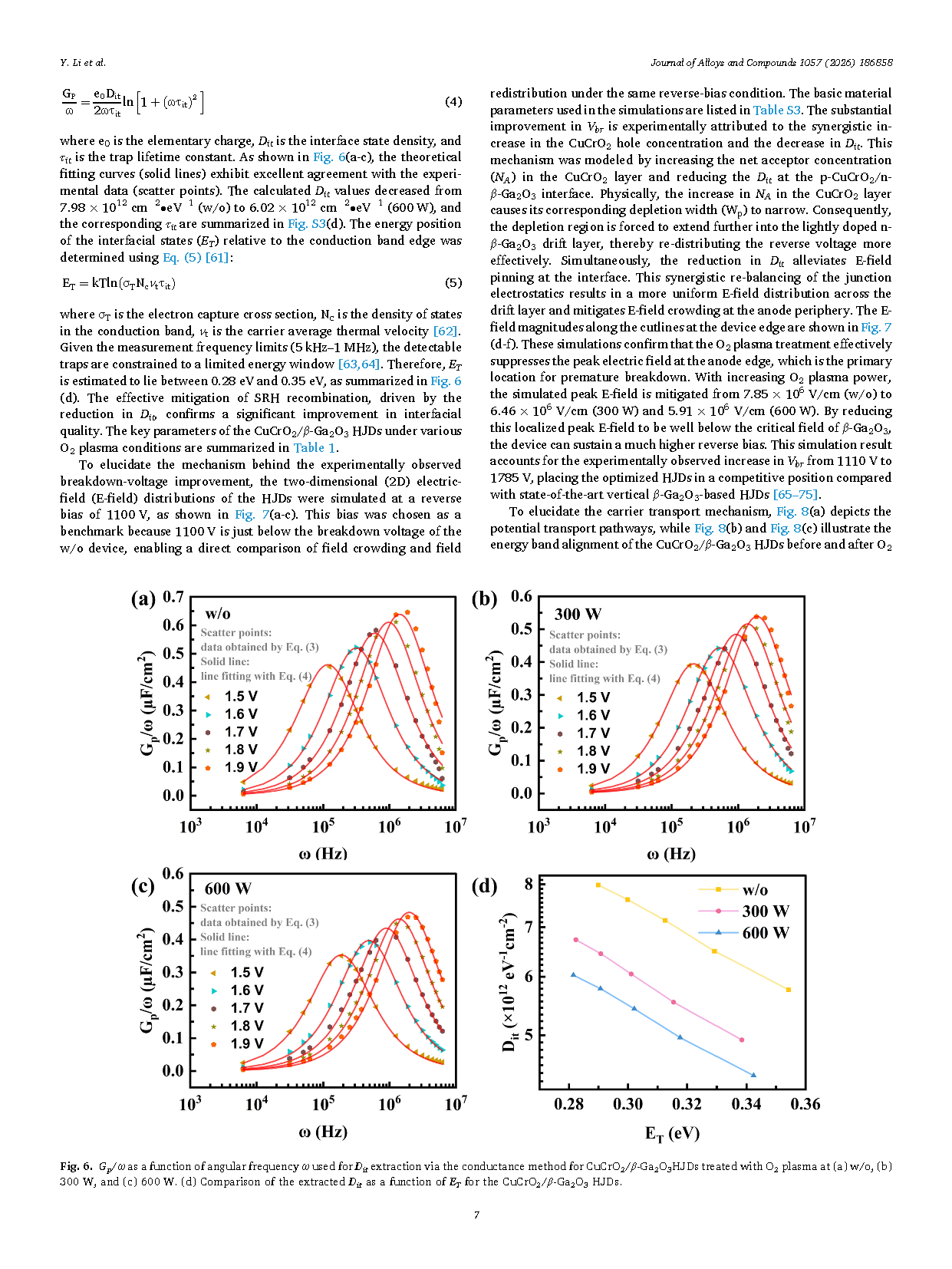
Figure 6.Gp/ω as a function of angular frequency (ω) for extracting interface trap density (Dit) of CuCrO₂/β-Ga₂O₃ HJDs using the conductance method after O₂ plasma treatment at (a) w/o, (b) 300 W, and (c) 600 W.(d) Comparison of extracted Dit as a function of trap energy level (ET).
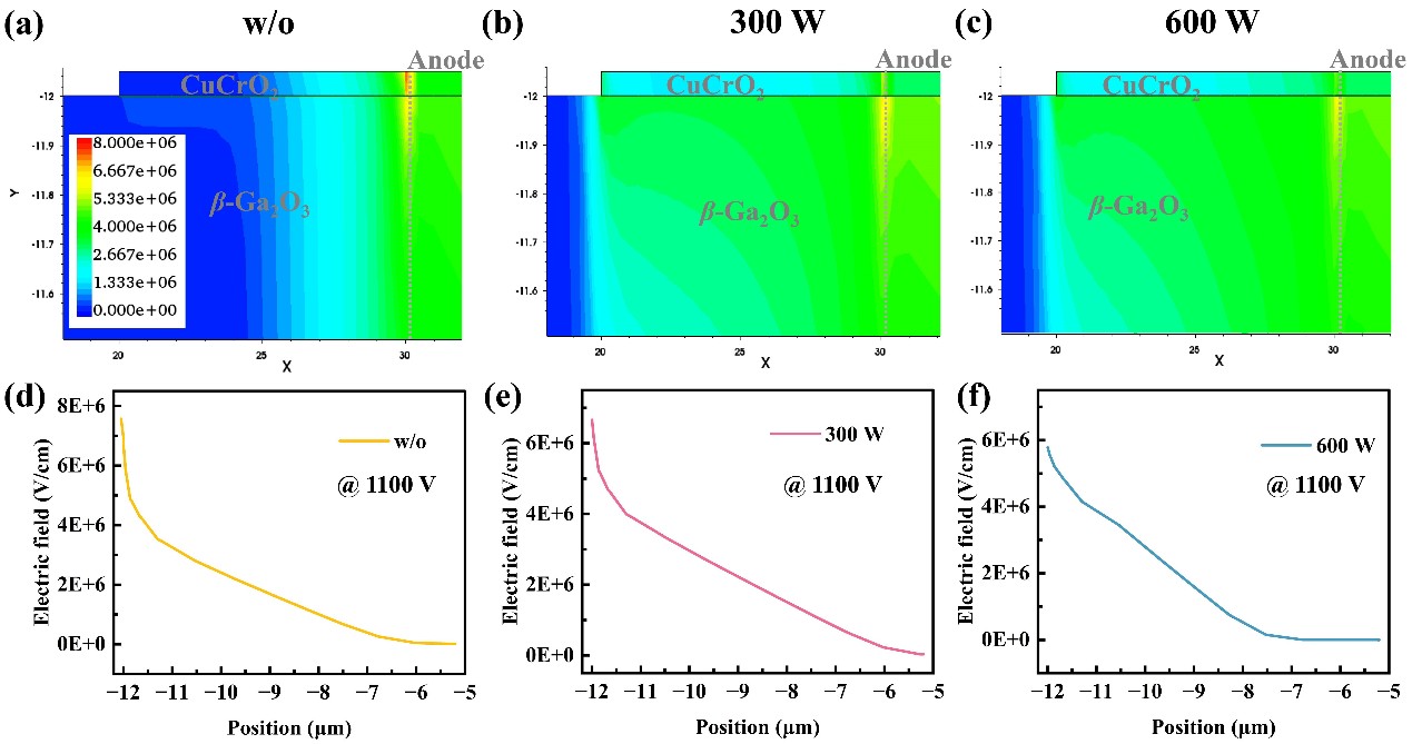
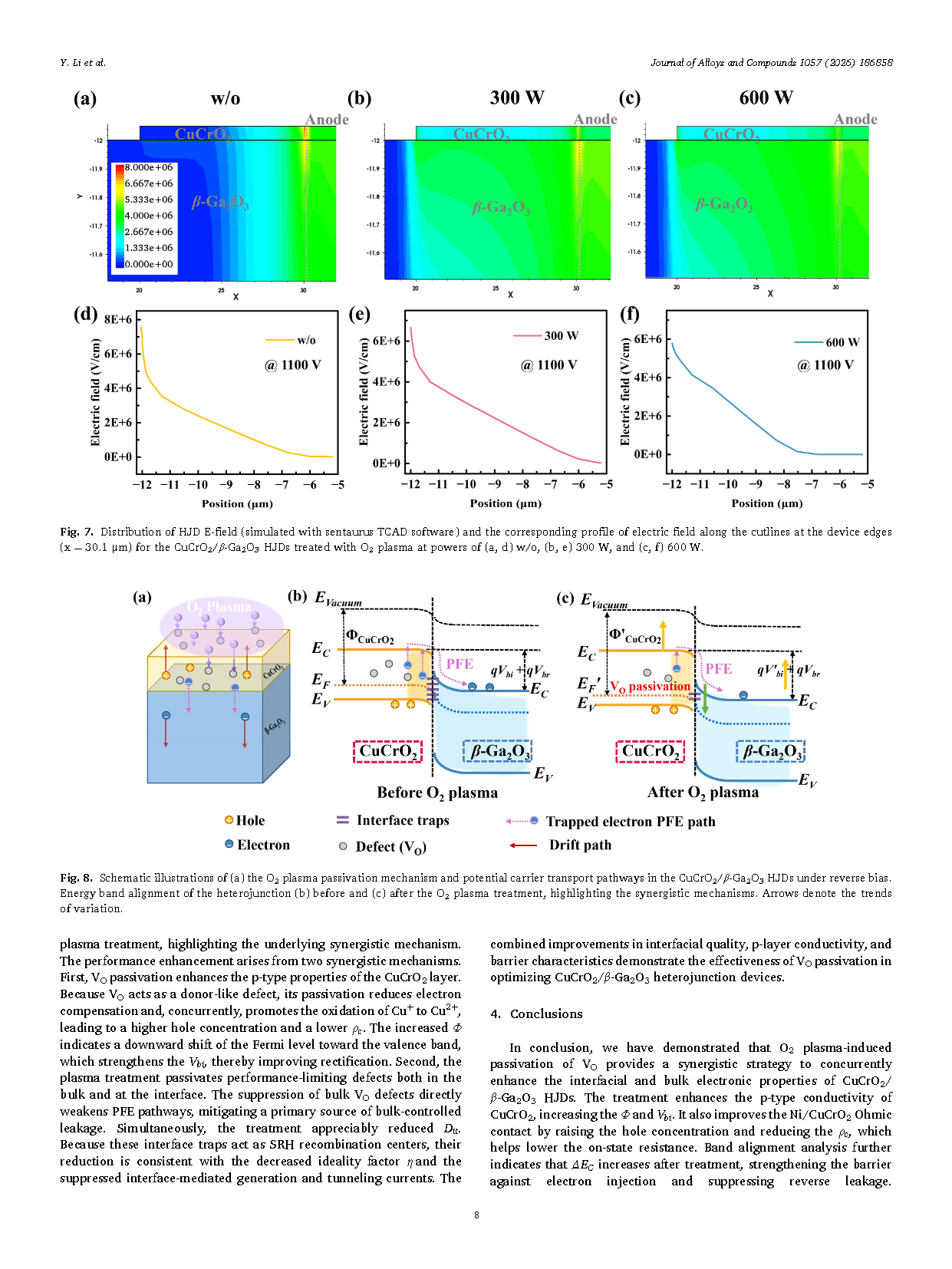
Figure 7.Electric field distribution of CuCrO₂/β-Ga₂O₃ HJDs (simulated using Sentaurus TCAD) after O₂ plasma treatment at (a, d) w/o, (b, e) 300 W, and (c, f) 600 W. The corresponding electric field profiles along the cutline at the device edge (x = 30.1 μm) are also shown.
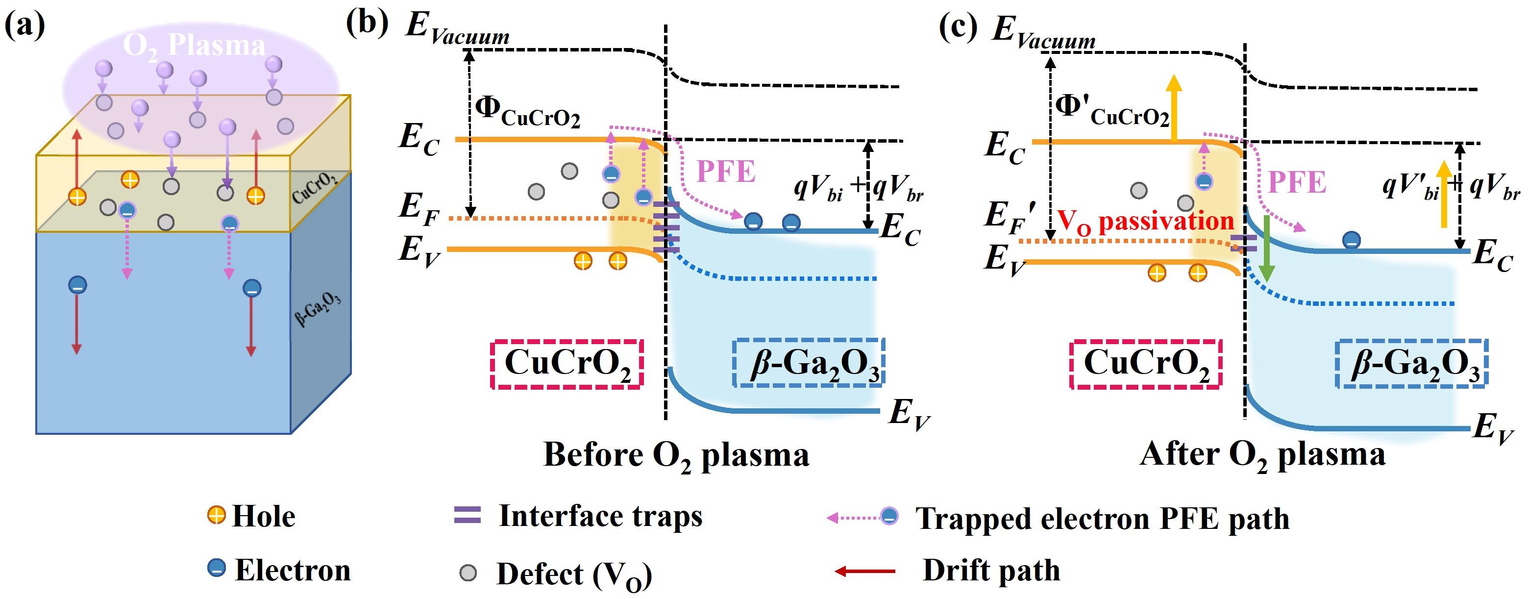
Figure 8.(a) Schematic illustration of the O₂ plasma passivation mechanism and carrier transport paths in CuCrO₂/β-Ga₂O₃ HJDs under reverse bias.(b, c) Energy band alignment of the heterojunction before and after O₂ plasma treatment, highlighting the synergistic mechanism. Arrows indicate the direction of changes.
DOI:
doi.org/10.1016/j.jallcom.2026.186858