Paper Sharing
【Member Papers】Amorphous InHfZnO/Ga₂O₃ heterojunction by plasma-enhanced atomic layer deposition for transparent photoelectric synaptic devices with temperature-tunable mechanism analysis
日期:2026-03-30阅读:141
Researchers from the Fudan University have published a dissertation titled "Amorphous InHfZnO/ Ga2O3 heterojunction by plasma-enhanced atomic layer deposition for transparent photoelectric synaptic devices with temperature-tunable mechanism analysis" in Optics Letters.
Background
In recent years, numerous advanced optical materials have been applied in photoelectric synaptic devices, including indium-based oxide semiconductors, hafnium-based oxide dielectric insulators, 2D materials, and the fourth-generation semiconductor Ga2O3. To further improve the performance of synaptic devices, these materials have been comprehensively integrated into heterojunction structures to leverage the advantages of individual materials. Moreover, to expand the applications of photoelectric synaptic devices, transparent devices based on these optical materials have been explored for specific scenes, including invisible devices and augmented reality technology. Among the materials mentioned above, indium-based oxides typically exhibit superior conductivity with effective UV absorption characteristics, while Ga2O3 is a promising photoelectric material widely applied in solar-blind photodetectors with superior performance, both of which showcase superior transparency in the visible region. For indium-based oxides, Zn is a critical dopant for enhancing thin film stability and UV optical absorption because of its ionic radius similarity to indium compared to other dopants, while Hf as a common dopant has the highest dissociation energy of Hf-O bonds among all dopants, both resulting in the development of indium hafnium zinc oxide (InHfZnO) thin films. By utilizing advanced plasma-enhanced atomic layer deposition (PEALD) technology, thin films of both Ga2O3 and InHfZnO materials can be deposited with high uniformity, high conformity, and low thermal budget, paving the way for high-performance photoelectric synaptic devices.
Abstract
Artificial photoelectric synaptic devices have exhibited remarkable advantages of low power consumption and high speed for neuromorphic computing. By integrating photo detection and memory functions, these devices offer a promising framework to resolve the limitations of von Neumann architectures. Herein, transparent photoelectric synaptic de vices were fabricated based on amorphous InHfZnO/Ga2O3 heterojunction by plasma-enhanced atomic layer deposition. The heterojunction was comprehensively characterized with various techniques. For the fabricated devices, critical synaptic characteristics, including short-term plasticity (STP), paired-pulse facilitation (PPF), and long-term plasticity (LTP), were systematically characterized and evaluated under various optical conditions and temperatures. Based on temperature-dependent performance variations, the temperature-tunable mechanism of the devices was analyzed in terms of oxygen vacancy concentration evolution.
Highlights
The amorphous indium hafnium zinc oxide was combined with gallium oxide, a fourth-generation semiconductor, to construct a heterojunction for the first time, which fully integrates the advantages of the two materials.
The InHfZnO/Ga2O3 heterojunction was fabricated by plasma-enhanced atomic layer deposition technology, achieving the deposition of thin films with high uniformity, high conformality and low thermal budget.
The prepared transparent photoelectric synaptic devices can effectively simulate the synaptic behavior of human vision with excellent performance in key synaptic characteristic parameters.
Systematic characterizations of this type of transparent photoelectric synaptic devices were carried out for the first time at multiple temperatures including room temperature, 37 °C (human body temperature) and 50 °C, clarifying the regulatory law of temperature on device performance.
Conclusion
In this research, transparent photoelectric synaptic devices based on the amorphous (InHfZnO/Ga2O3) heterojunction were fabricated via PEALD and comprehensively characterized. XPS, TEM, XRD, and optical characterizations of the as deposited heterojunction confirmed its suitability for photoelectric synaptic applications, with favorable structure, chemical state, and optical properties. Electrical and photoelectric characterizations demonstrated the feasible performance of the fabricated devices effectively simulating human visual synaptic behavior, with a PPF index over 170%. Moreover, photoelectric characterizations under higher temperatures were executed, showcasing temperature-dependent performance. The higher temperatures lead to higher photocurrent but shorter retention time. The temperature-tunable mechanism of the photoelectric performance variation was analyzed via in-situ XPS O 1s characterizations based on VO concentration variation.
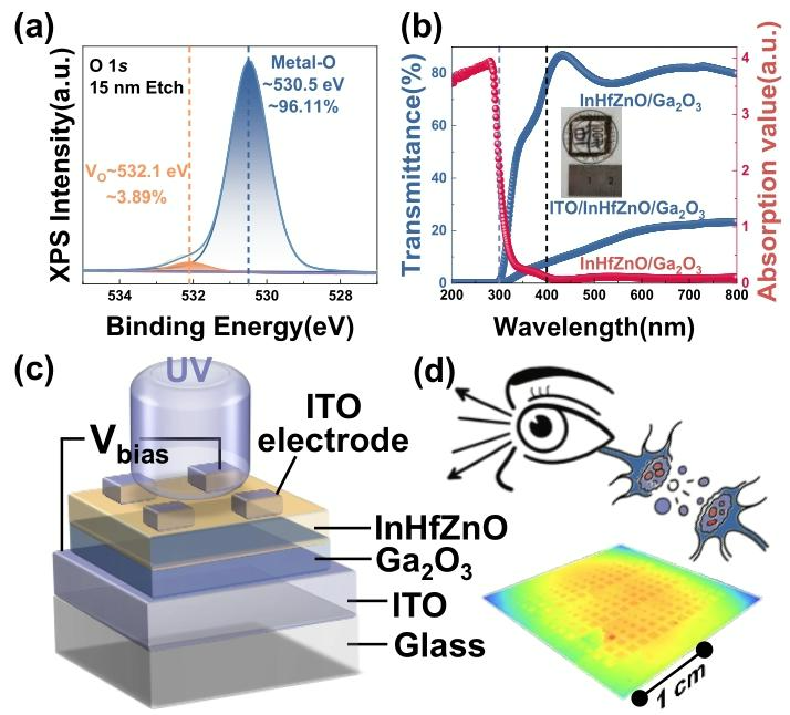
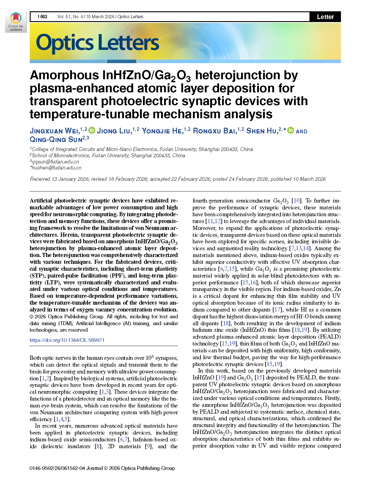
Fig. 1. (a) The XPS O 1s peak deconvolution of the (InHfZnO/Ga2O3) heterojunction after 15-nm etch processing. (b) The optical absorption and transmittance characterizations of the heterojunction on ITO conductive glass substrate, with the optical transmittance characterizations after the ITO electrode deposition. (c) The fabricated photoelectric synaptic device models. (d) The processes of the photodetection of human eyes and nerve conduction of the human optical nerve synapses with the surface optical image of the fabricated device.
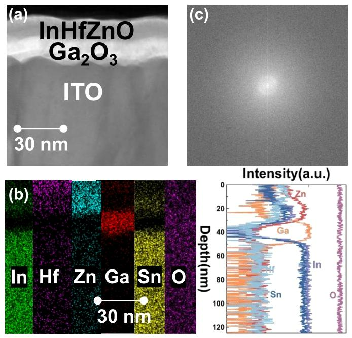
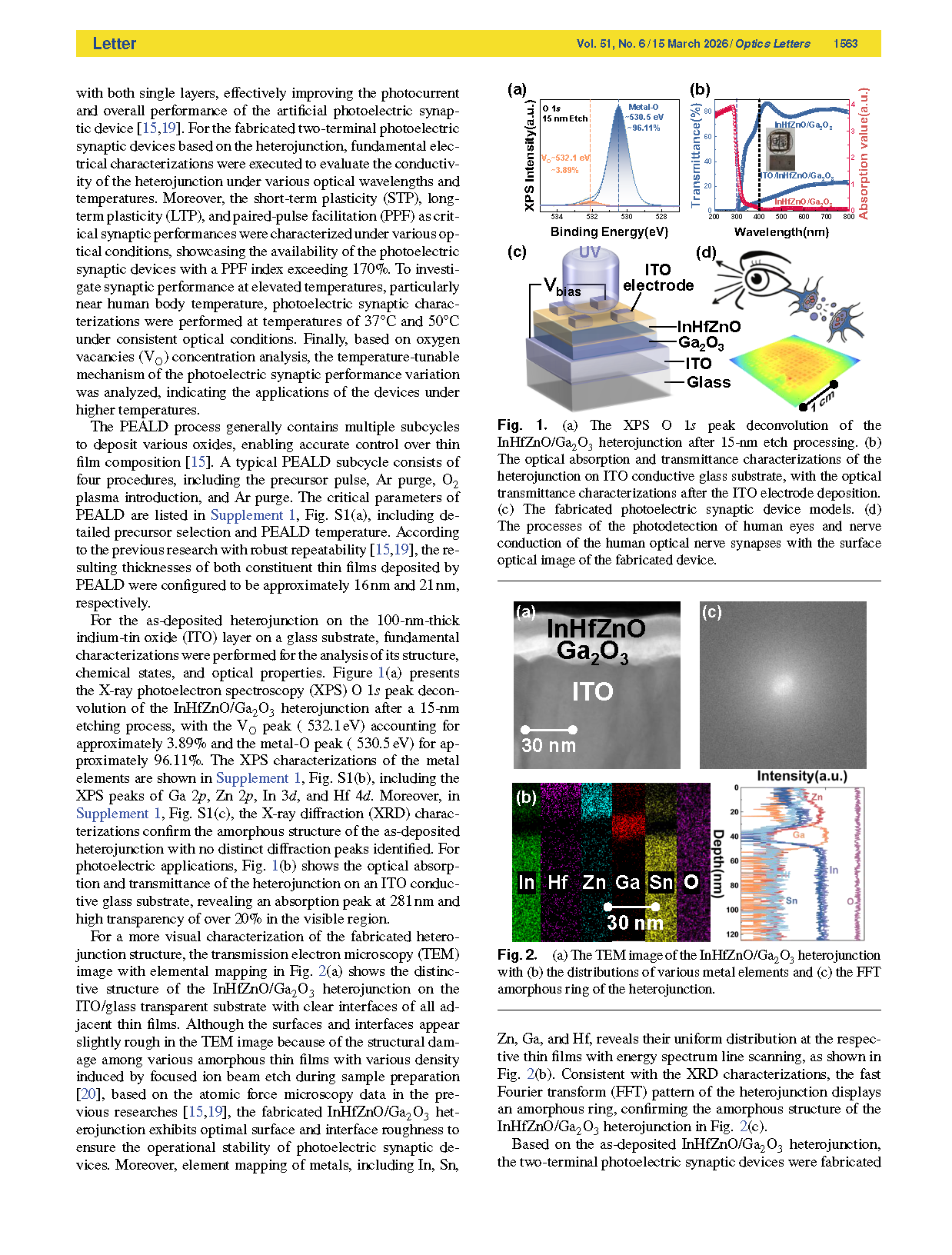
Fig.2. (a) The TEM image of the (InHfZnO/Ga2O3) heterojunction with (b) the distributions of various metal elements and (c) the FFT amorphous ring of the heterojunction.
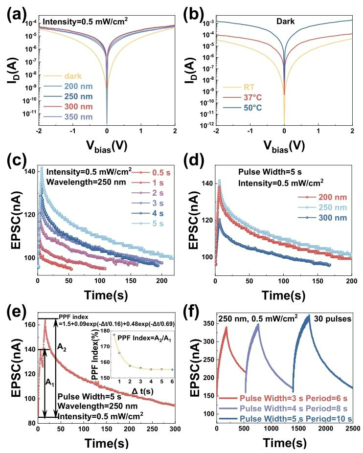
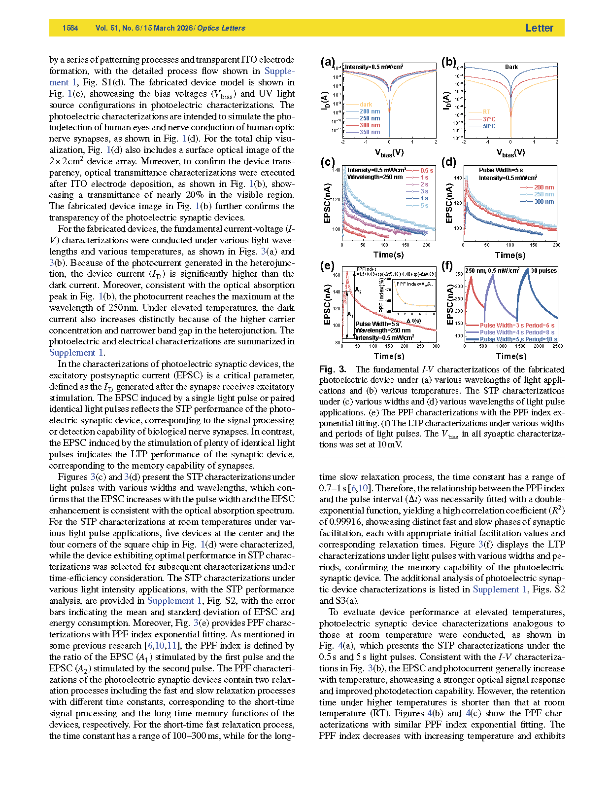
Fig. 3. The fundamental I-V characterizations of the fabricated photoelectric device under (a) various wavelengths of light applications and (b) various temperatures. The STP characterizations under (c) various widths and (d) various wavelengths of light pulse applications. (e) The PPF characterizations with the PPF index exponential fitting. (f) The LTP characterizations under various widths and periods of light pulses. The Vbias in all synaptic characterizations was set at 10 mV.
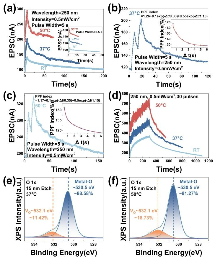
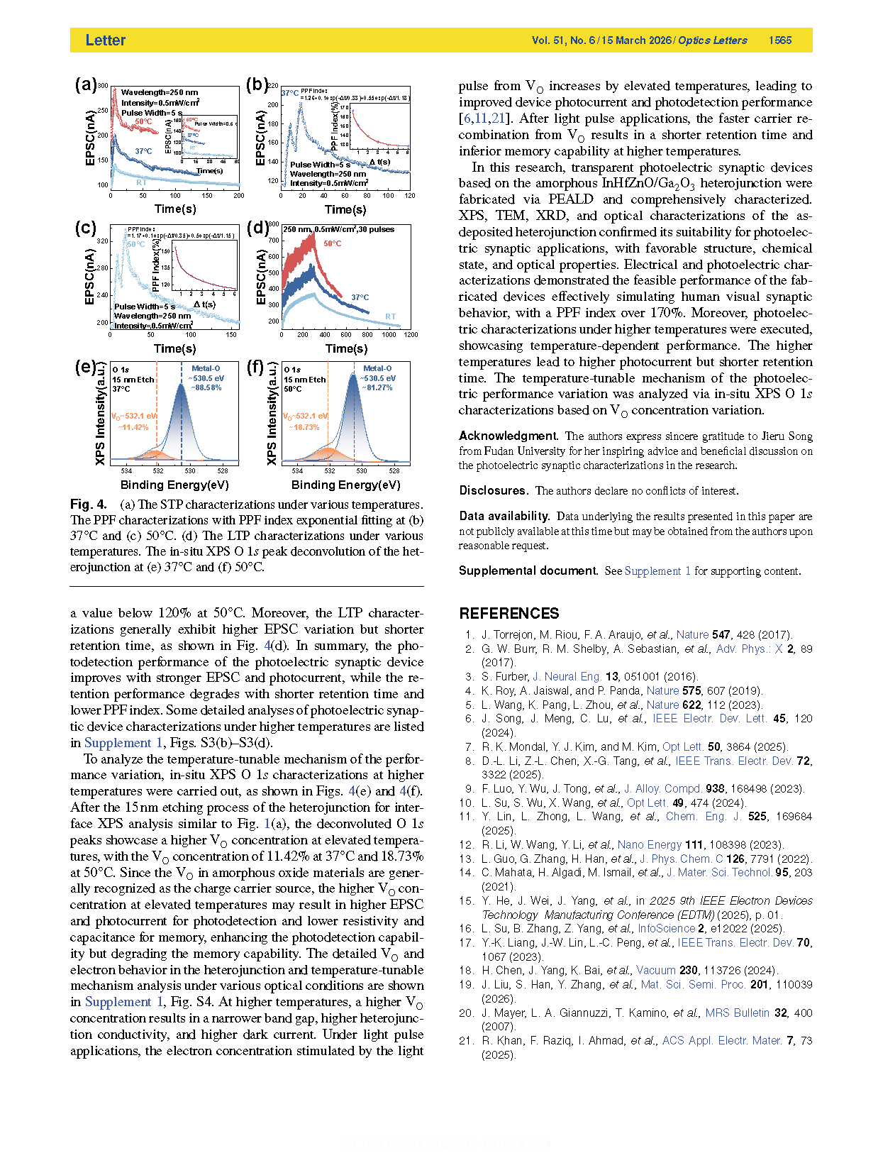
Fig. 4. (a) The STP characterizations under various temperatures. The PPF characterizations with PPF index exponential fitting at (b) 37°C and (c) 50°C. (d) The LTP characterizations under various temperatures. The in-situ XPS O 1s peak deconvolution of the heterojunction at (e) 37°C and (f) 50°C.
DOI:
doi.org/10.1088/2752-5724/ae4e4c