Paper Sharing
【Member Papers】Research of Schottky diode based on Ga₂O₃/SiC pn heterojunction RESURF structure
日期:2026-03-27阅读:187
Researchers from the Department of Electronic Engineering, Xi'an University of Technology; Key Laboratory of Wide Bandgap Semiconductor Materials, Ministry of Education, Xidian University; Shenzhen Pinghu Laboratory, National Wide Bandgap Semiconductor Technology Innovation Center (Shenzhen) have published a dissertation titled "Research of Schottky diode based on Ga₂O₃/SiC pn heterojunction RESURF structure" in Microelectronics Journal.
Background
Constrained by the bandgap width, the performance of traditional silicon-based devices is approaching the theoretical limit, which is difficult to meet the continuous demand for conversion efficiency of high-power electronic devices. As an ultra-wide bandgap semiconductor, Ga₂O₃ has become a core candidate material for next-generation power devices due to its bandgap of 4.5 ~ 4.9 eV, critical breakdown field strength of 8 MV/cm, high saturation electron velocity, and the advantage of low-cost preparation of large-size single crystal substrates. Its Baliga figure of merit far exceeds that of GaN, SiC and Si materials. However, Ga₂O₃ has problems such as difficulty in achieving effective p-type doping, low electron mobility, extremely low and anisotropic thermal conductivity (0.1~0.27 W/cm·K), resulting in the device breakdown voltage not reaching the theoretical value, and prone to performance drift and thermal accumulation failure. As a wide bandgap semiconductor, SiC can accurately regulate the p-type doping concentration, with a thermal conductivity as high as 3.7~4.9 W/cm·K. Heterogeneous integration with Ga₂O₃ can effectively solve the above bottlenecks. Meanwhile, the Reduced Surface Field (RESURF) technology can optimize the electric field distribution through charge sharing and alleviate the trade-off contradiction between breakdown voltage and on-resistance. Based on the research of Ga₂O₃/SiC heteroepitaxy, the team proposed a Schottky diode integrated with heterojunction pn-type RESURF structure and optimized the device performance through TCAD simulation.
Abstract
This work reports a Schottky diode with a RESURF (reduced surface field) termination formed by a p-SiC / n-Ga₂O₃ heterojunction. The device characteristics were investigated using TCAD simulation software. The results demonstrate that the RESURF SBD achieves a specific on-resistance (Ron,sp) of 25.604 mΩ·cm² and an enhanced breakdown voltage of 1666 V, compared to 1086 V for a Ga₂O₃ homojunction device. The power figure of merit (PFOM) reaches 0.108 GW/cm². Subsequently, the influence of the n-type Ga₂O₃ drift layer thickness, p-type field drop layer (FDL) thickness, and FDL doping concentration on the electrical characteristics was systematically studied. Additionally, the peak temperature induced by the self-heating effect decreased from 387 K to 315 K, accompanied by a significantly improved temperature distribution. This diode utilizes the Ga₂O₃/SiC heterojunction p-n structure to form the RESURF configuration, thereby enhancing the breakdown voltage and improving the forward conduction characteristics. The high thermal conductivity SiC substrate is employed to mitigate the issue of the low thermal conductivity of the Ga₂O₃ material.
Highlights
● Structural Innovation
Firstly proposed a Schottky diode with Ga₂O₃/SiC pn heterojunction coupled RESURF structure, breaking through the structural limitations of traditional Ga₂O₃ devices.
● Performance Improvement
The breakdown voltage is increased from 1086 V to 1666 V, and the power figure of merit reaches 0.108 GW/cm², taking into account high voltage resistance and low loss.
● Thermal Management Optimization
Using high thermal conductivity SiC substrate, the peak temperature of the device is reduced by 72 K, the thermal distribution is more uniform, and the self-heating effect is alleviated.
● Systematic Parameter Optimization
Clarified the regulation law of drift layer thickness, field drop layer thickness and doping concentration on device performance, and obtained the optimal breakdown voltage of 1814 V.
● Clear Mechanism
Revealed the modulation mechanism of the vertical electric field of the heterojunction on the surface electric field, and explained the core principle of the RESURF structure to improve the voltage resistance.
Conclusion
Addressing the fundamental challenges of the lack of viable p-type doping and extremely low thermal conductivity in Ga₂O₃, this work proposes a Ga₂O₃ SBD incorporating RESURF technology. The device achieves a breakdown voltage of 1666 V, a Ron,sp of 25.604 mΩ·cm², and a PFOM of 0.108 GW/cm². When the drift region thickness is 0.9 μm, the field reduction layer thickness is 1μm, and the doping concentration is 3×10¹⁶ cm⁻³, the device achieves a maximum breakdown voltage of 1812 V. Under this condition, Ron,sp is 28.212 mΩ·cm², and the PFOM reaches 0.116 GW/cm². Furthermore, the temperature distribution is significantly improved, reducing the peak device temperature from 387 K to 315 K. A systematic analysis was conducted on the influence of drift region thickness, FDL thickness, and FDL doping concentration, identifying their specific impacts on device characteristics and achieving a maximum BV of 1814 V. However, due to the relatively thick drift region and its low doping concentration, the drift region remains incompletely depleted during device blocking and the Ron,sp is not sufficiently low during conduction. This limits the full manifestation of the RESURF principle's potential for high breakdown voltage and low loss. Consequently, future work will focus on implementing additional structural features and optimizing geometric parameters to further enhance the high-voltage blocking capability and minimize conduction losses.
Project Support
This work was supported by the National Natural Science Foundation of China, Young Talent Fund of Xi'an Association for Science and Technology, Science and technology planning project of Xi'an, Youth Science and Technology Star Project of Shaanxi Province, and China Postdoctoral Science Foundation Project.
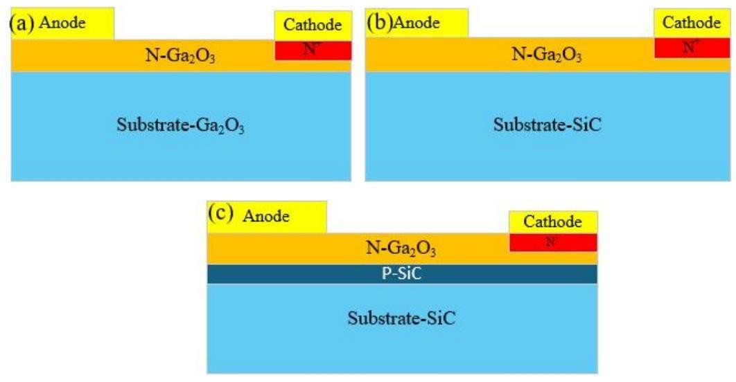
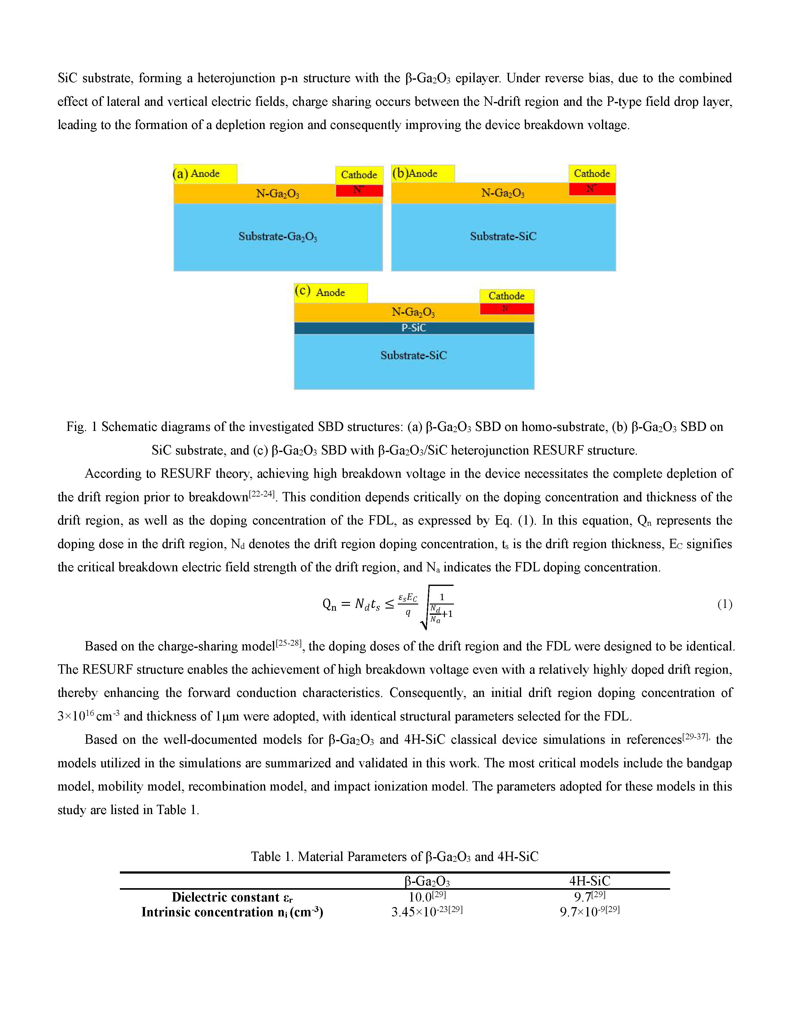
Fig. 1 Schematic diagrams of the investigated SBD structures: (a) β-Ga₂O₃ SBD on homo-substrate, (b) β-Ga₂O₃ SBD on SiC substrate, and (c) β-Ga₂O₃ SBD with β-Ga₂O₃/SiC heterojunction RESURF structure.
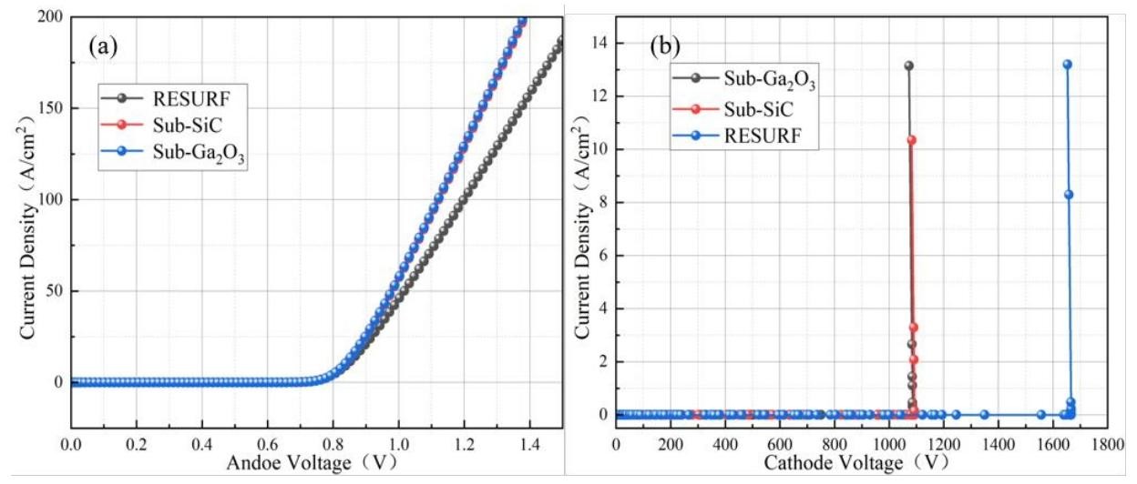
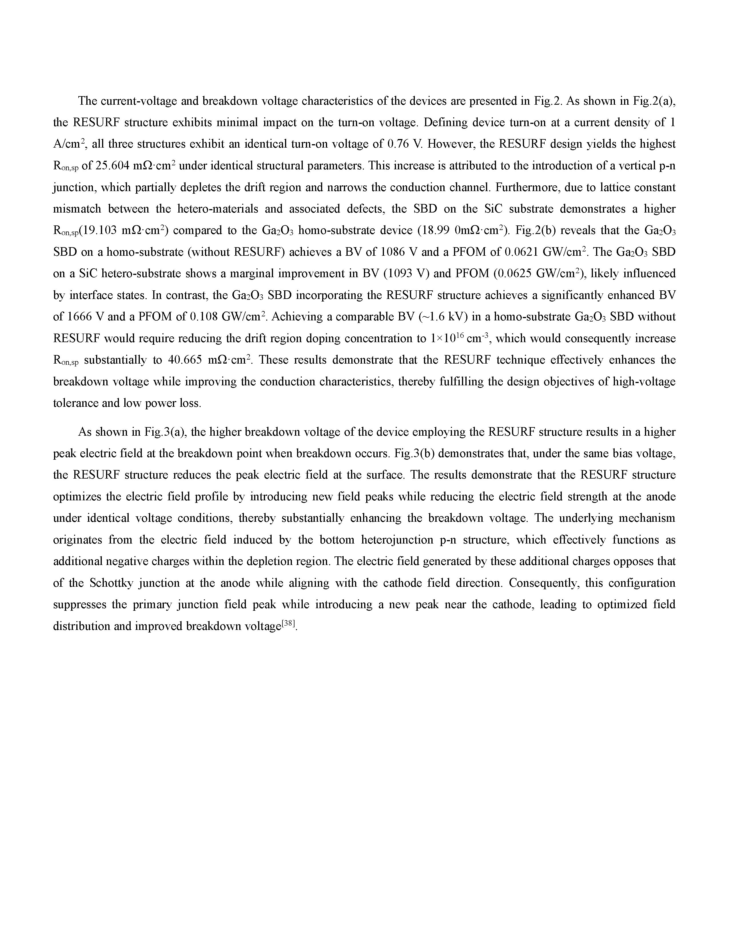
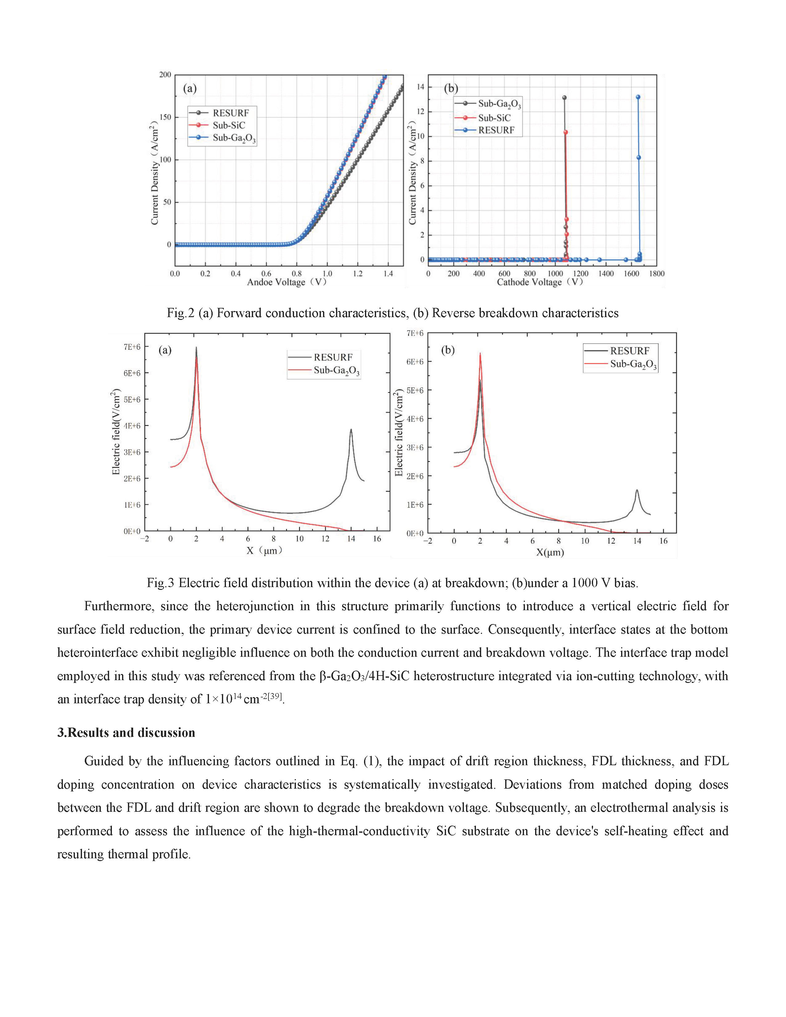
Fig.2 (a) Forward conduction characteristics, (b) Reverse breakdown characteristics.
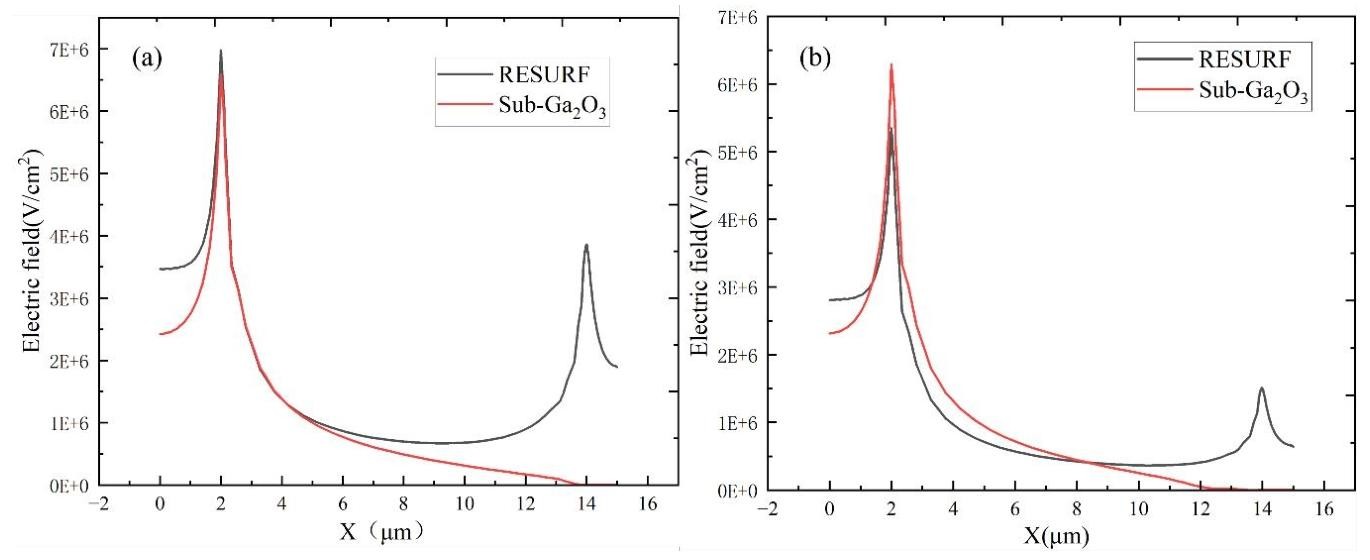
Fig.3 Electric field distribution within the device (a) at breakdown; (b)under a 1000 V bias.
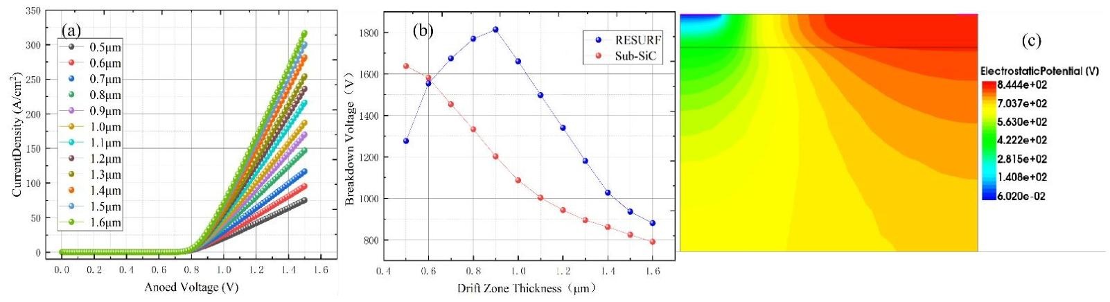
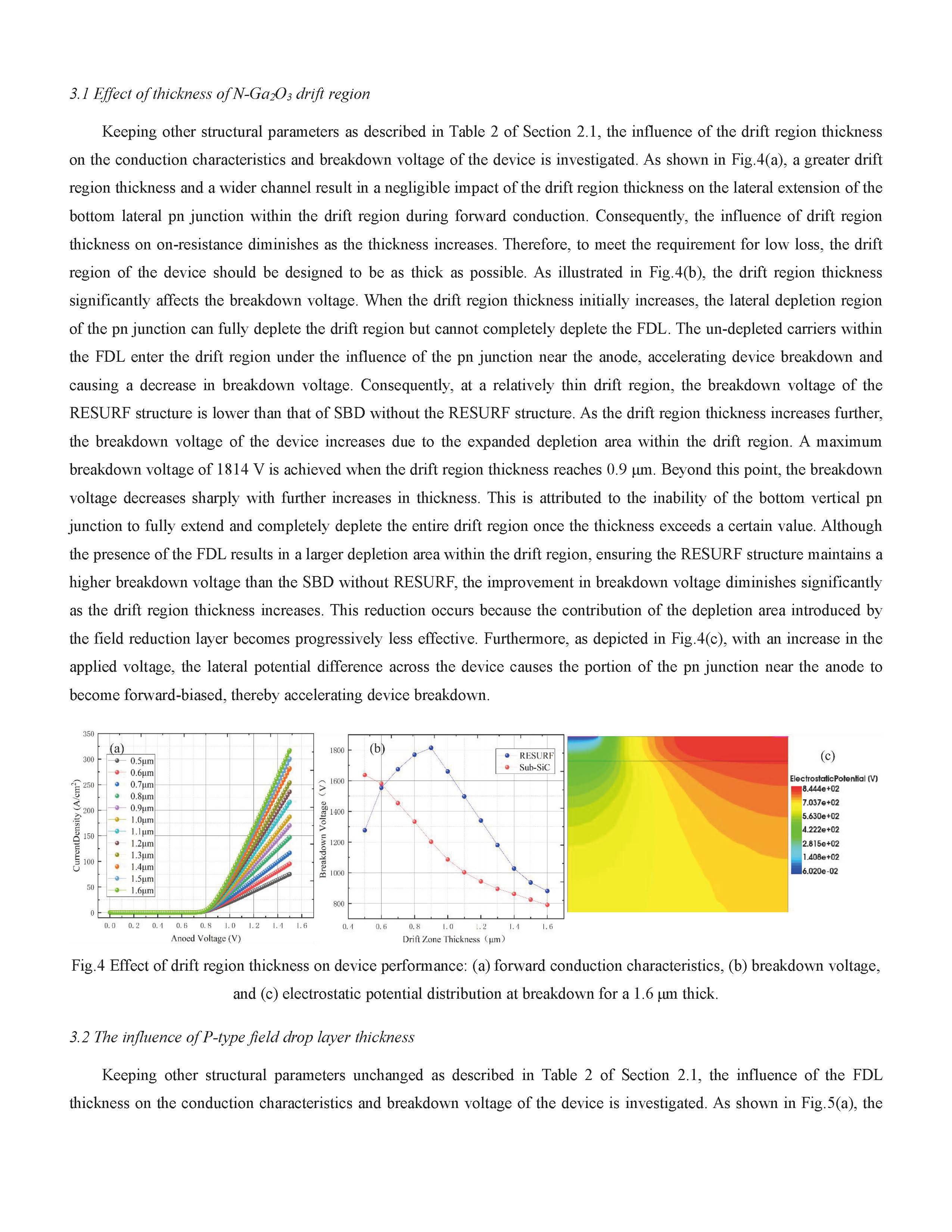
Fig.4 Effect of drift region thickness on device performance: (a) forward conduction characteristics, (b) breakdown voltage, and (c) electrostatic potential distribution at breakdown for a 1.6 μm thick.
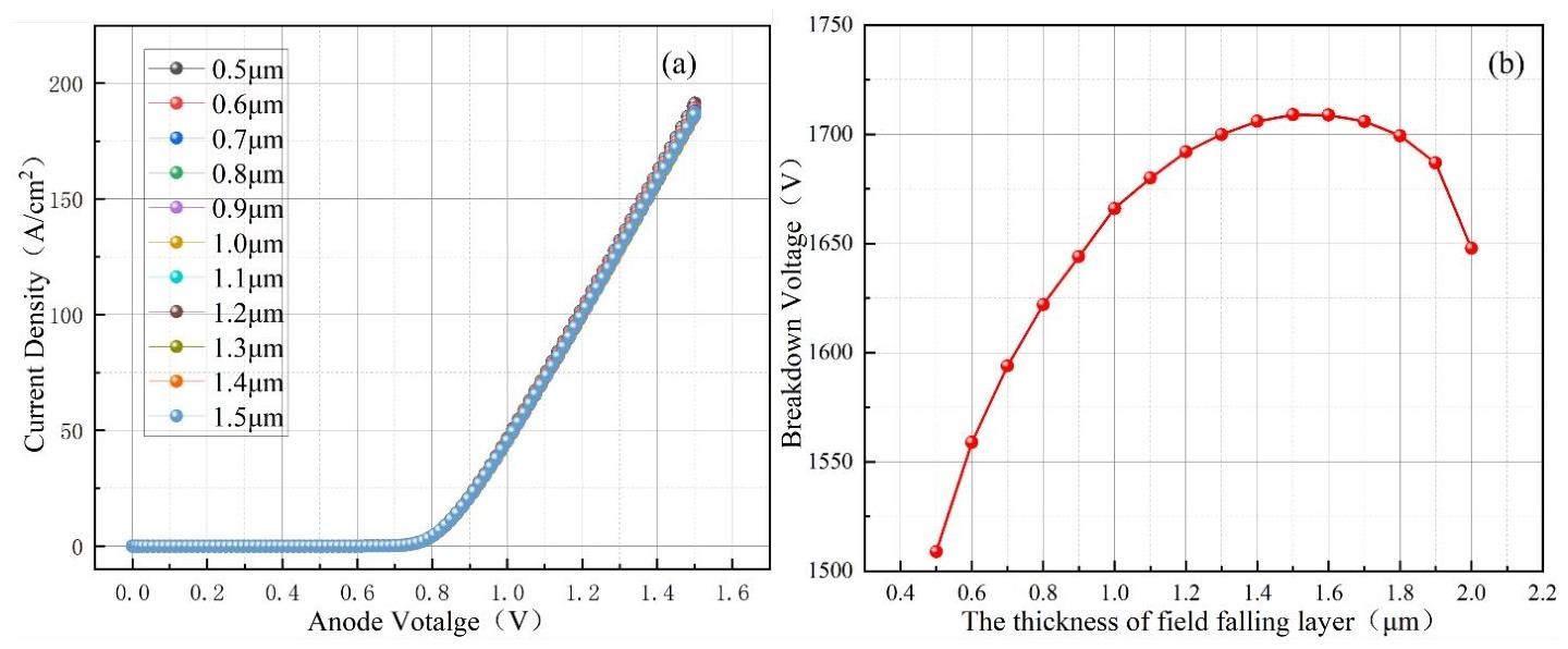
Fig.5 The influence of field-drop layer thickness on device characteristics (a)forward conduction characteristics, (b) breakdown voltage.
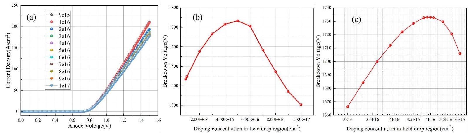
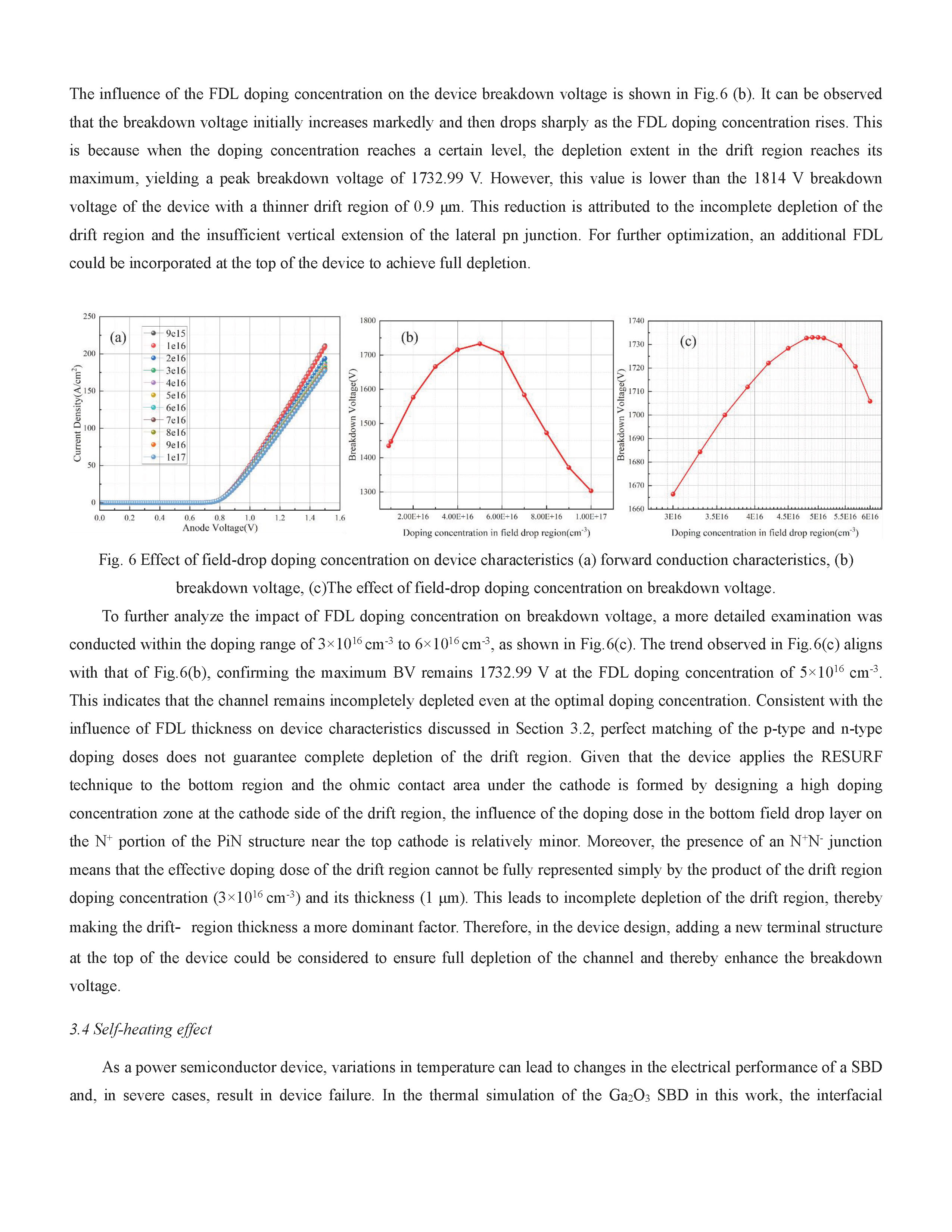
Fig. 6 Effect of field-drop doping concentration on device characteristics (a) forward conduction characteristics, (b) breakdown voltage, (c)The effect of field-drop doping concentration on breakdown voltage.
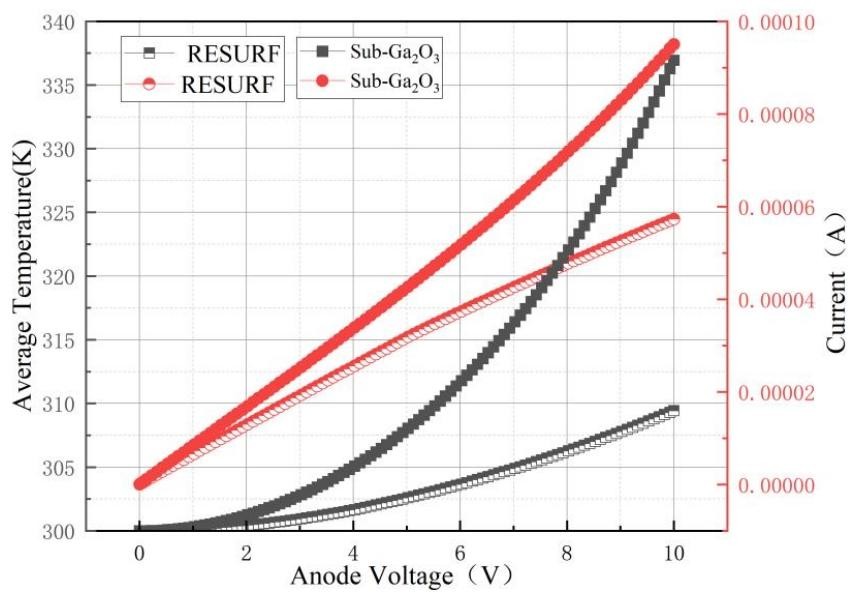
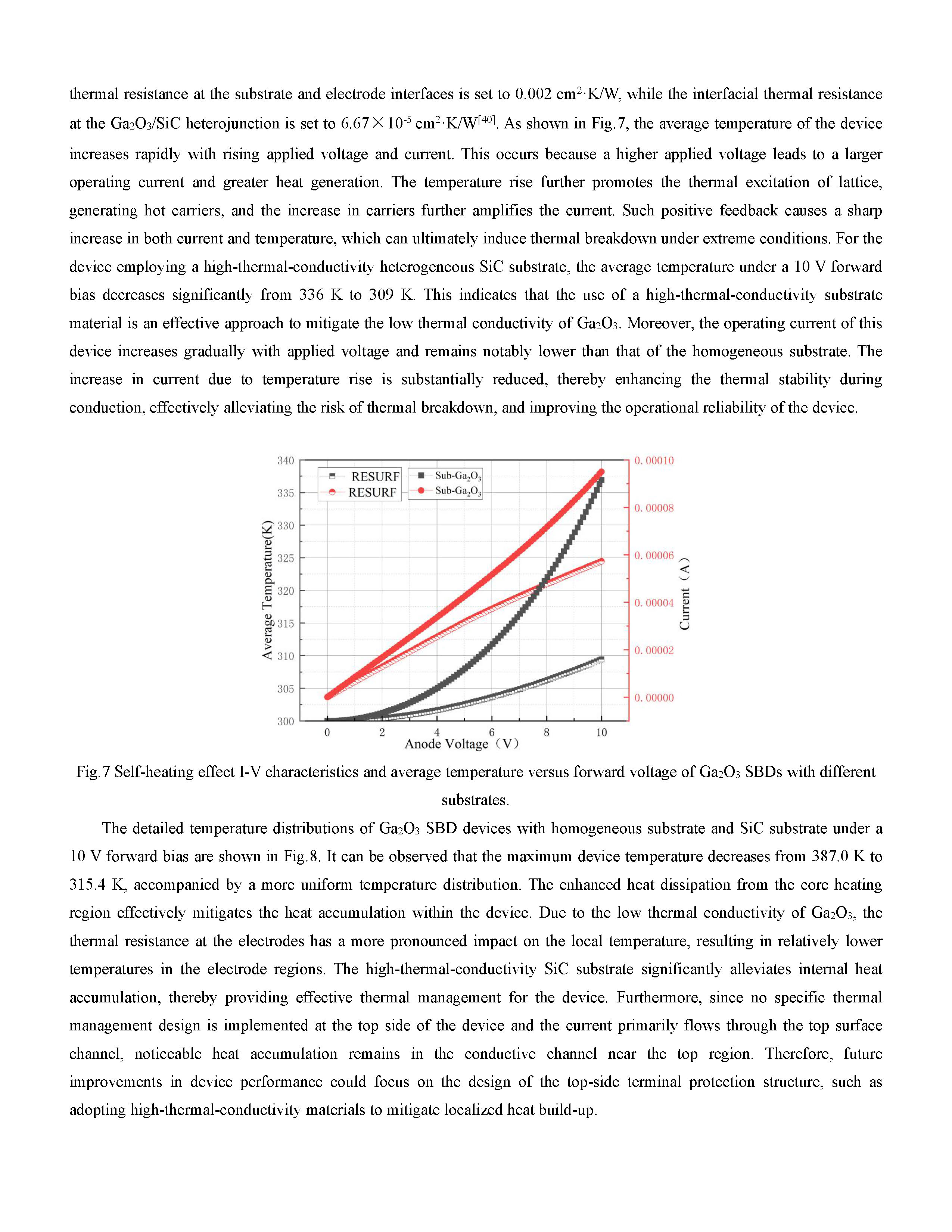
Fig.7 Self-heating effect I-V characteristics and average temperature versus forward voltage of Ga₂O₃ SBDs with different substrates.
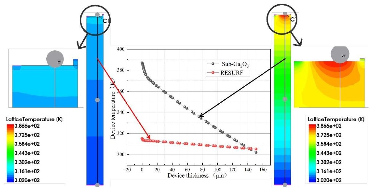
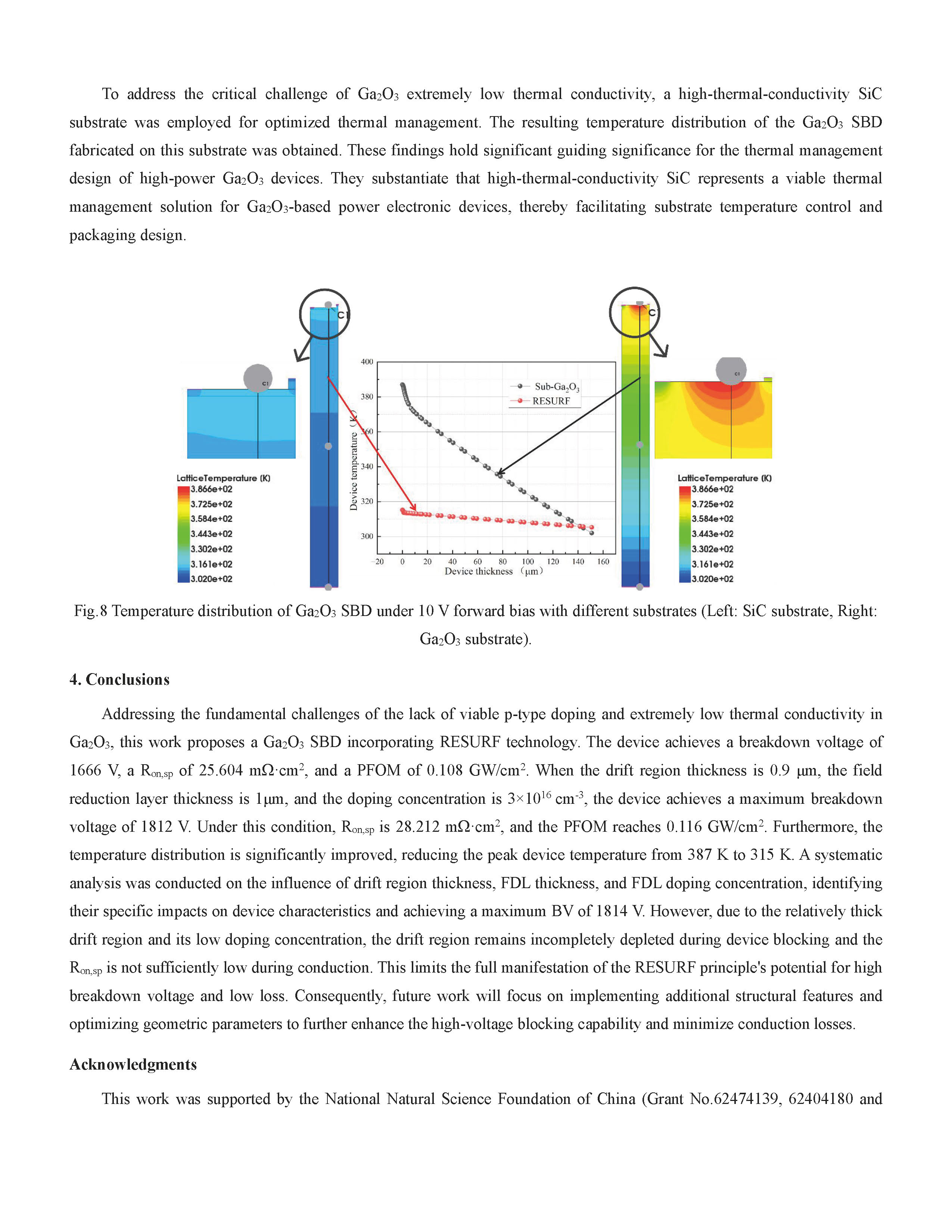
Fig.8 Temperature distribution of Ga₂O₃ SBD under 10 V forward bias with different substrates (Left: SiC substrate, Right: Ga₂O₃ substrate).
DOI:
https://doi.org/10.1016/j.mejo.2026.107173