Paper Sharing
【Member Papers】4.1/3.5 kV Breakdown Voltage in Depletion/Enhancement-Mode MOCVD-Grown Ga₂O₃ MOSFETs on Sapphire Substrates
日期:2026-03-26阅读:223
Researchers from the research team led by Professor Genquan Han and Associate Professor Yibo Wang of Xidian University, in collaboration with Associate Researcher Jun Zheng of the Institute of Semiconductors, Chinese Academy of Sciences, have published a dissertation titled "4.1/3.5 kV Breakdown Voltage in Depletion/Enhancement-Mode MOCVD-Grown Ga₂O₃ MOSFETs on Sapphire Substrates" in Japanese Journal of Applied Physics.
Background
β-Gallium oxide (β-Ga₂O₃) is a key power semiconductor material with a wide bandgap of approximately 4.8~4.9 eV, providing superior breakdown voltage characteristics for high electric field operations. Advanced epitaxial technologies such as molecular beam epitaxy and metal-organic chemical vapor deposition (MOCVD) allow for the preparation of high-quality conductive channels, enabling the development of high-performance power metal-oxide-semiconductor field-effect transistors (MOSFETs). Research on Ga₂O₃ homoepitaxial power MOSFETs has shown significant electrical performance, with the breakdown voltage of vertical β-Ga₂O₃ transistors achieving above 2.6 kV and lateral β-Ga₂O₃ transistors exceeding 10 kV. Currently, 4-inch semi-insulating Ga₂O₃ homoepitaxial substrates have been reported, with progress toward 6-inch semi-insulating substrates. However, their low thermal conductivity and the degradation of electrical characteristics with rising temperature pose challenges for Ga₂O₃ power devices. Additionally, Ga₂O₃ homoepitaxial substrates are very expensive.
The sapphire substrate is a promising platform for preparing Ga₂O₃ conductive channels and power MOSFETs due to its low cost, large size and commercial availability. Most reported Ga₂O₃ MOSFETs on sapphire adopt in-situ Si doping, but the epitaxial layer has massive grain distortions such as twins and stacking faults, leading to unsatisfactory forward and breakdown characteristics. Fluorine-plasma surface doping can enhance channel conductivity, but the high volatility of fluorine in β-Ga₂O₃ limits doping efficiency. The poor quality of heteroepitaxial Ga₂O₃ films, insufficient conductivity and simple device structures severely restrict device performance. The team carried out research to break through the performance bottleneck of heteroepitaxial devices.
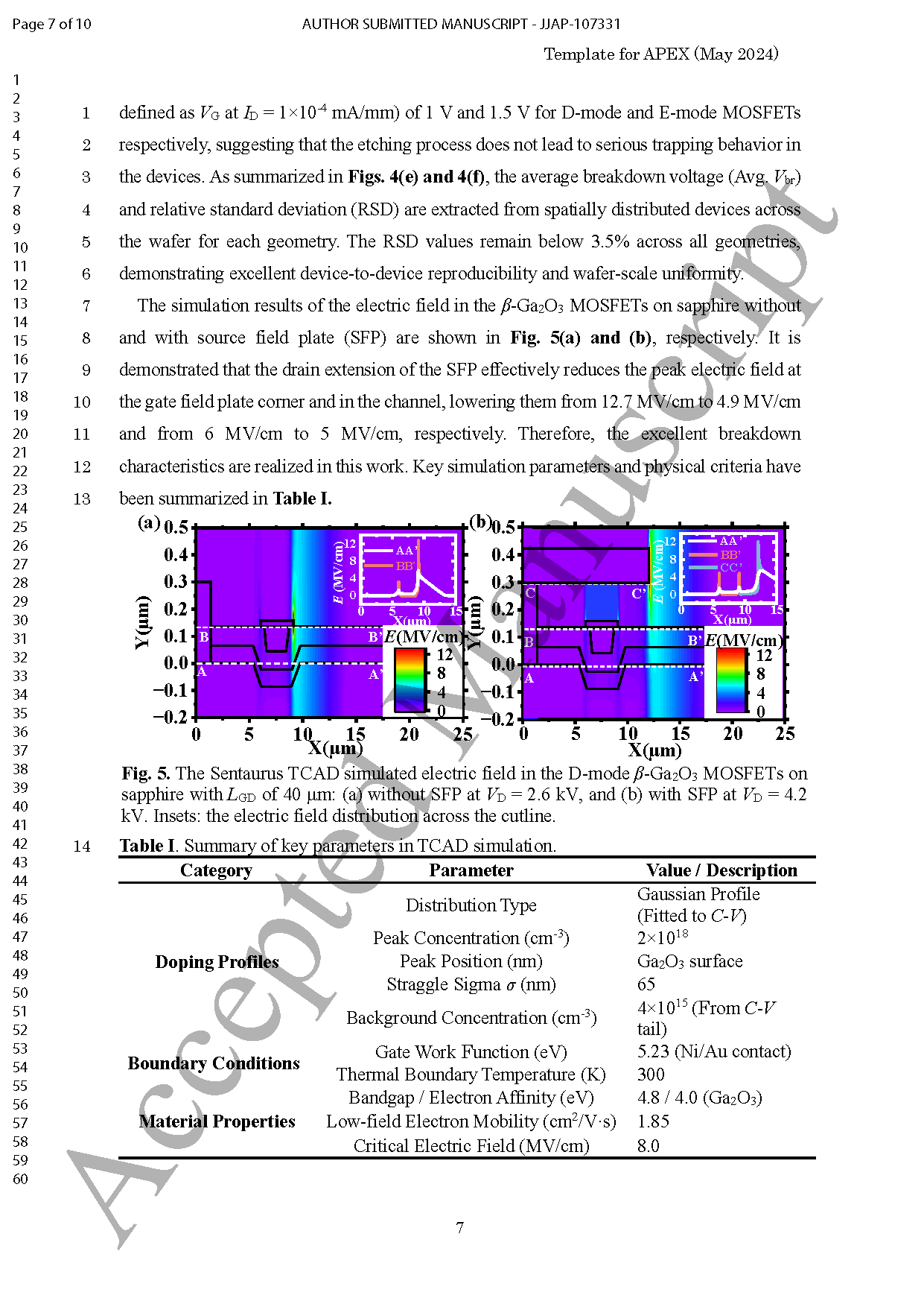
Abstract
In this work, we realized high-performance β-Ga₂O₃ power MOSFETs grown via MOCVD on sapphire substrates. HRXRD and HRTEM characterization confirmed single crystallinity of the β-Ga₂O₃ heteroepitaxial film on c-plane sapphire. Low-damage Si⁺ ion implantation followed by annealing was conducted to enhance conductivity. Utilizing a recessed channel architecture, we fabricated both D-mode and E-mode β-Ga₂O₃ MOSFETs. The inclusion of source and gate field plates, and thick gate trench dielectric yielded the breakdown voltage (Vbr) of 4129 V and 3509 V for D-mode and E-mode devices respectively. Both device types demonstrate breakdown characteristics comparable to homoepitaxial β-Ga₂O₃ MOSFETs, while surpassing previously reported heteroepitaxial counterparts on sapphire substrates.
Highlights
High-quality heteroepitaxial film preparation
The team grew single-crystal β-Ga₂O₃ films on sapphire substrates via MOCVD, with dislocations distributed discontinuously to effectively block vertical leakage paths.
Low-damage doping for enhanced conductivity
Low-damage Si⁺ ion implantation combined with annealing was adopted to realize impurity activation, transforming semi-insulating films into conductive films with a carrier concentration of 2×10¹⁸ cm⁻³.
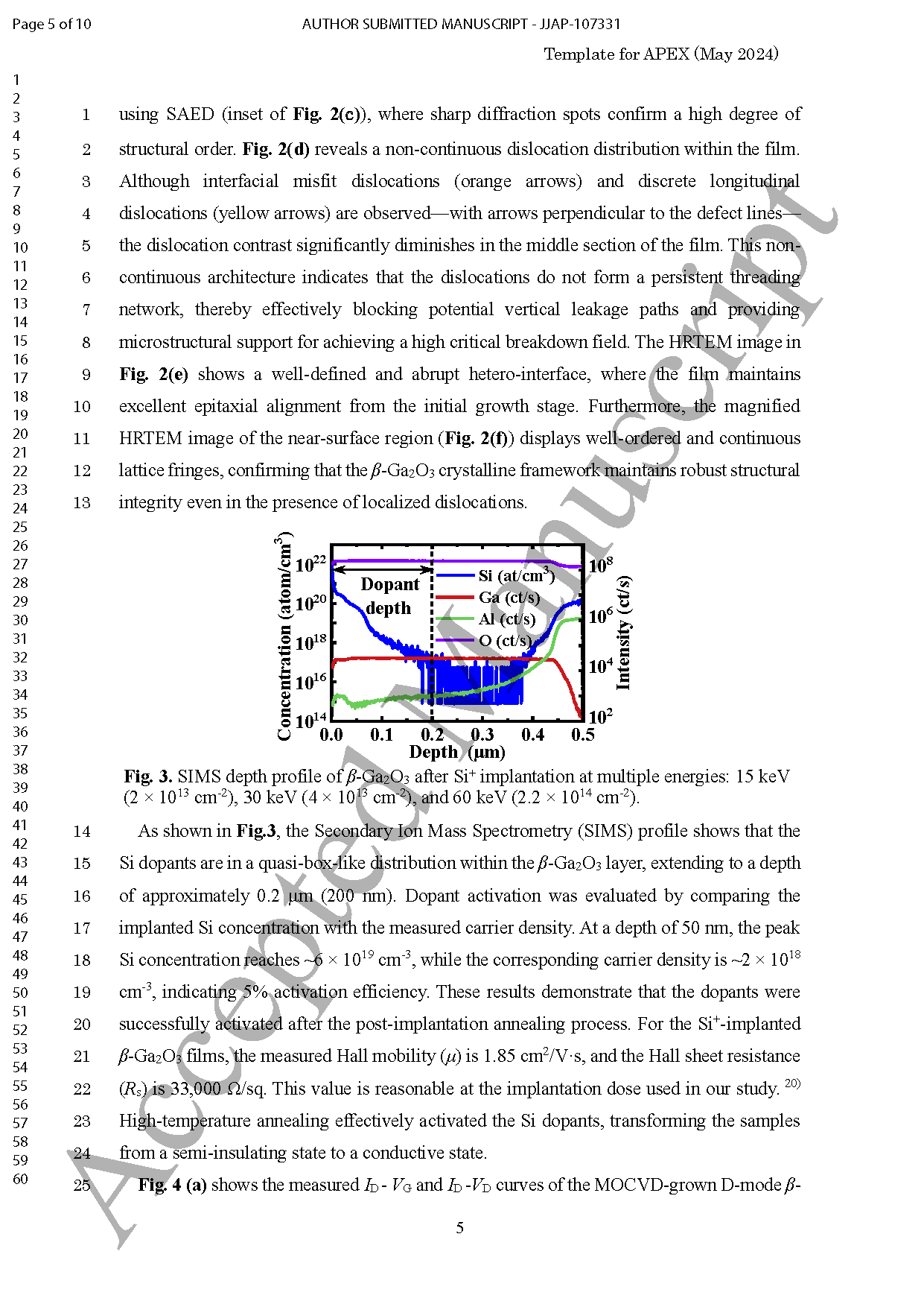
Dual-mode device fabrication
By adjusting the recess etching depth, both depletion-mode and enhancement-mode β-Ga₂O₃ MOSFETs were realized synchronously with extremely small threshold voltage hysteresis.
Ultra-high breakdown voltage breakthrough
Combined with source/gate dual field plates and thick gate trench dielectric structure, the breakdown voltage reaches 4129 V for D-mode devices and 3509 V for E-mode devices, setting a new record for sapphire-based heteroepitaxial devices.
Excellent device uniformity
The relative standard deviation of wafer-level device breakdown voltage is less than 3.5%, showing good uniformity for mass production.
Conclusion
In this study, we successfully demonstrated high-performance MOCVD-grown β-Ga₂O₃ power MOSFETs on sapphire substrates. Low-damage Si⁺ ion implantation followed by annealing increased carrier density and thus enhanced conductivity. Utilizing a recessed channel architecture, we achieved both D-mode and E-mode devices. By employing source, gate field plates, and TGTD structure, the high Vbr of 4129 V for D-mode and 3509 V for E-mode devices were realized. Compared to reported D-mode β-Ga₂O₃ MOSFETs on sapphire, our devices on sapphire exhibited significantly improved Vbr vs. RON,sp performance. The fabricated D-mode and E-mode heteroepitaxial devices realized comparable Vbr characteristics to those in homoepitaxial Ga₂O₃ MOSFETs, while surpassing previously reported heteroepitaxial counterparts on sapphire substrates.
Project Support
This work was supported by the National Natural Science Foundation of China, Strategic leading science and technology project of CAS, and the Fundamental Research Funds for the Central Universities.
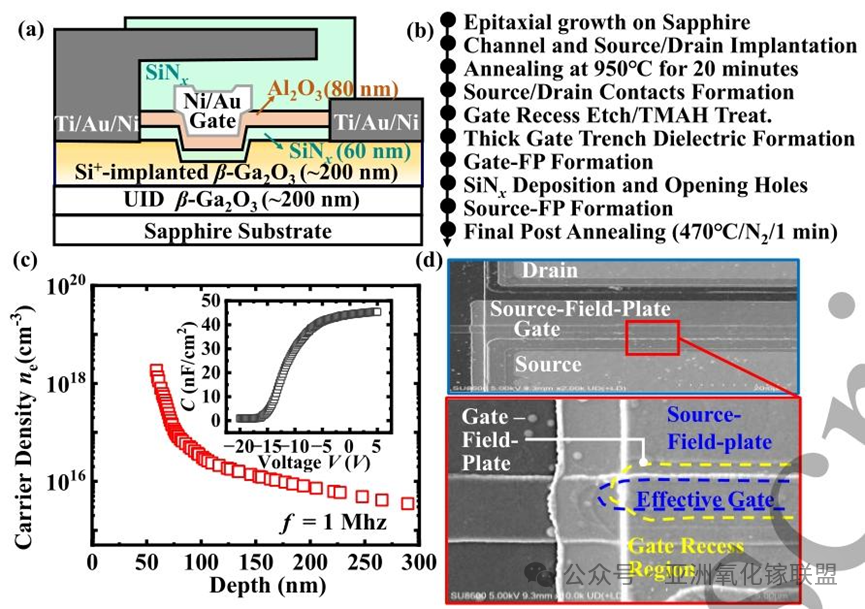
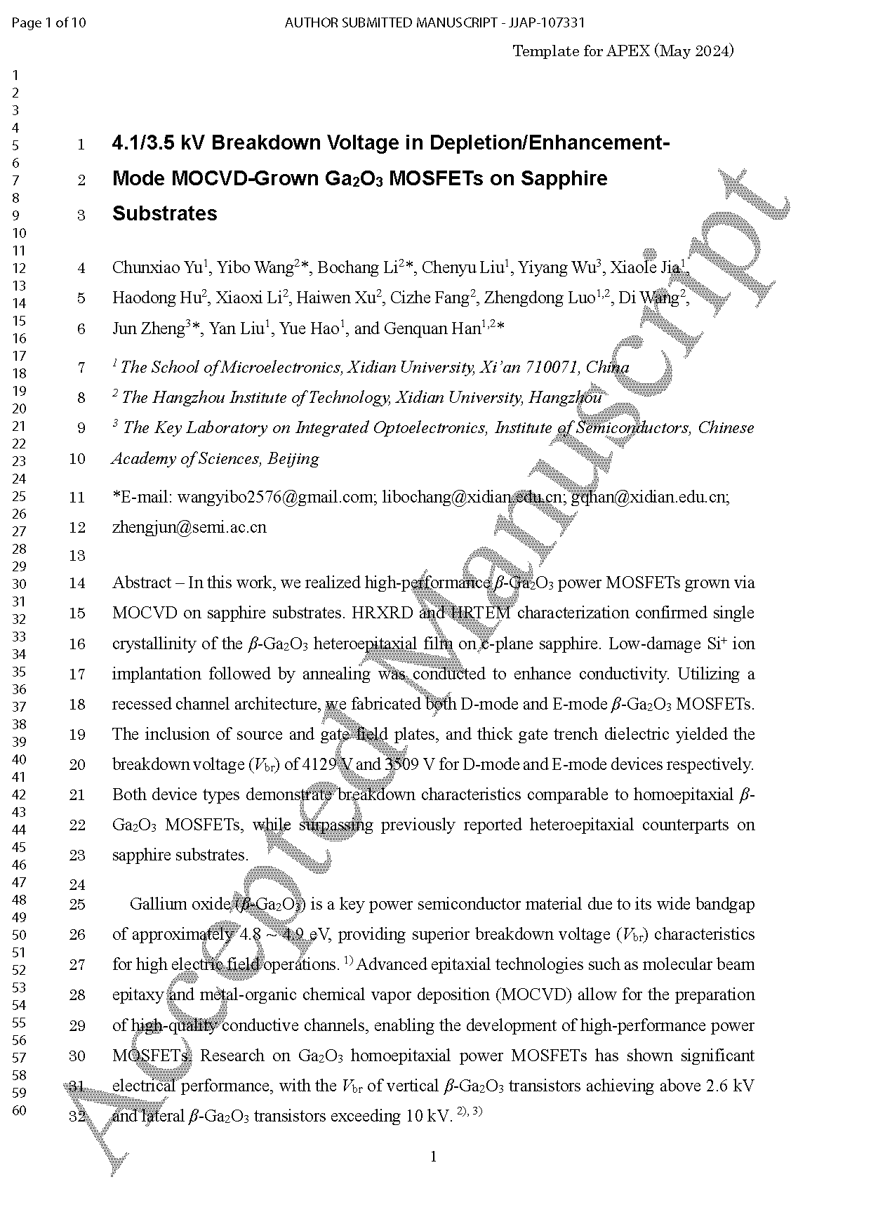
Fig. 1. (a) A schematic of the fabricated β-Ga₂O₃ MOSFETs on sapphire, illustrating the (b) key process steps for fabricating the devices. UID stands for unintentionally doped. (c) Carrier distribution profile extracted from the C-V measurement (inset) of the SiNₓ/β-Ga₂O₃ MOS capacitor at 1 MHz. (d) An SEM image of the device, showing the drain, source, source field plate, and gate regions.

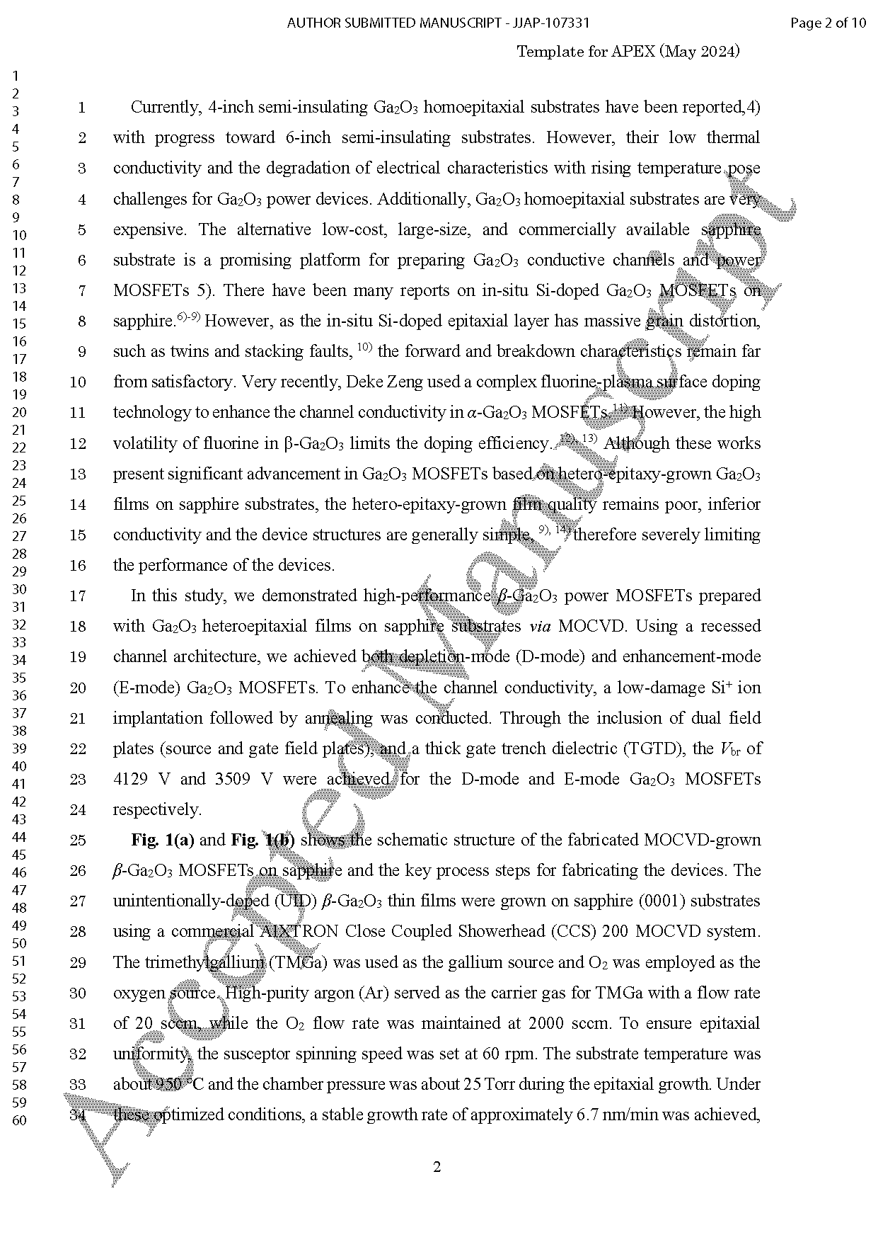
Fig. 2. (a) XRD 2θ–ω spectra of MOCVD-grown β-Ga₂O₃ films on sapphire. (b) Rocking curves of β-Ga₂O₃ after Si⁺ ion implantation; inset: measurement points across the wafer. Cross-sectional TEM images of β-Ga₂O₃/sapphire after implantation: (c) overview with SAED (inset); (d) dislocation distribution, where orange and yellow arrows indicate interface misfit and longitudinal dislocations, respectively; (e) interface HRTEM; (f) near-surface β-Ga₂O₃ HRTEM showing high crystallinity.
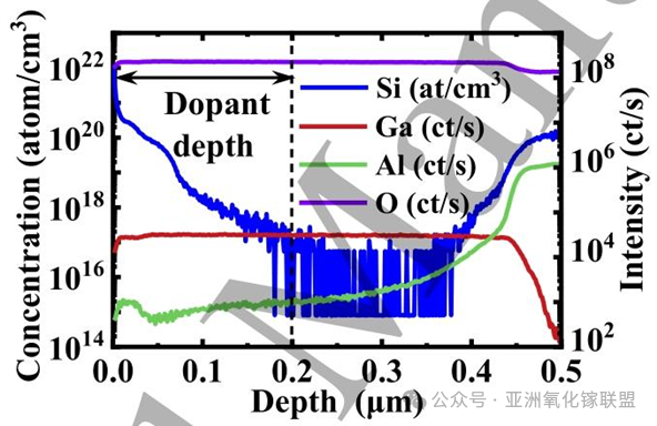
Fig. 3. SIMS depth profile of β-Ga₂O₃ after Si⁺ implantation at multiple energies: 15 keV (2×10¹³ cm⁻²), 30 keV (4×10¹³ cm⁻²), and 60 keV (2.2×10¹⁴ cm⁻²).
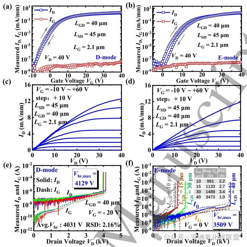
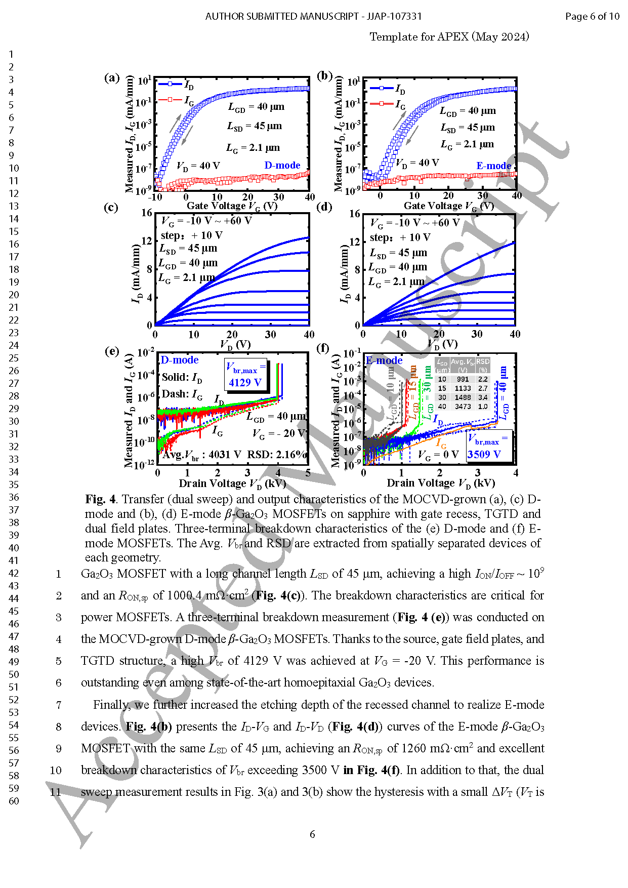
Fig. 4. Transfer (dual sweep) and output characteristics of the MOCVD-grown (a), (c) D-mode and (b), (d) E-mode β-Ga₂O₃ MOSFETs on sapphire with gate recess, TGTD and dual field plates. Three-terminal breakdown characteristics of the (e) D-mode and (f) E-mode MOSFETs. The Avg. Vbr and RSD are extracted from spatially separated devices of each geometry.
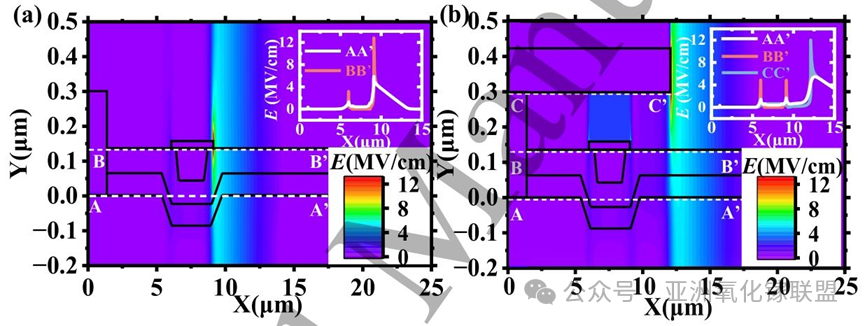
Fig. 5. The Sentaurus TCAD simulated electric field in the D-mode β-Ga₂O₃ MOSFETs on sapphire with LGD of 40 μm: (a) without SFP at VD=2.6 kV, and (b) with SFP at VD =4.2 kV. Insets: the electric field distribution across the cutline.
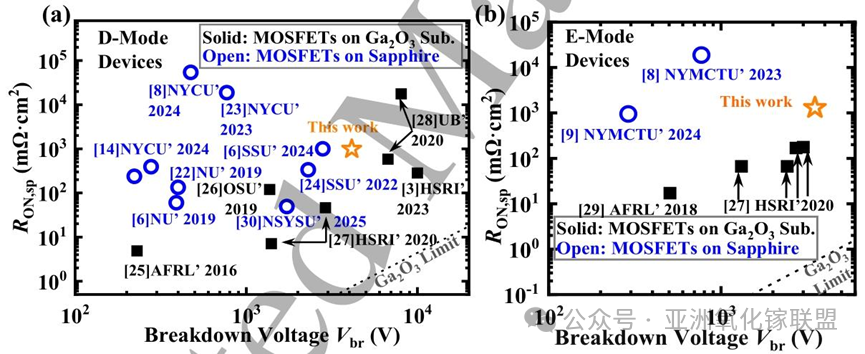
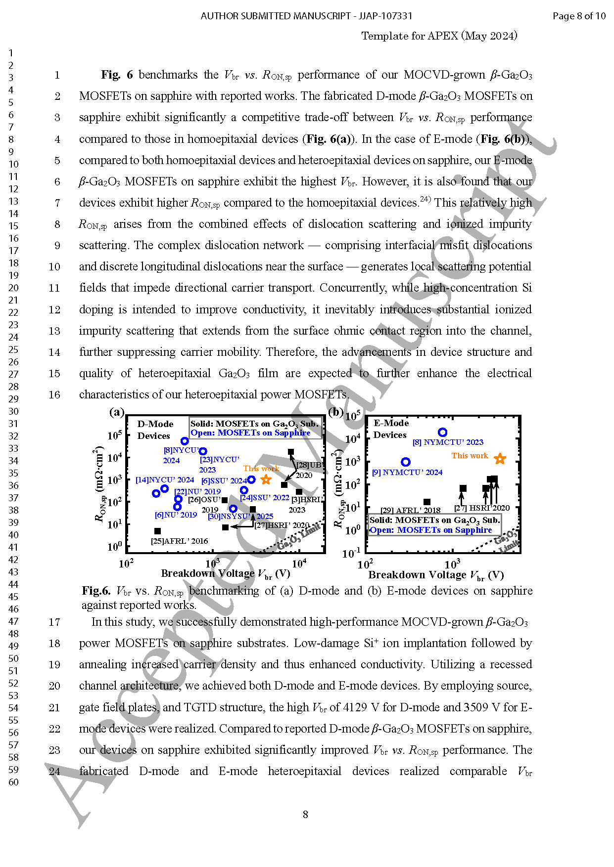
Fig. 6. Vbr vs. RON,sp benchmarking of (a) D-mode and (b) E-mode devices on sapphire against reported works.
DOI:
10.35848/1347-4065/ae51da