Paper Sharing
【Domestic Papers】Characteristics of gallium oxide nMOSFET inverter
日期:2026-03-25阅读:173
Researchers from the Xi’an University of Posts and Telecommunications have published a dissertation titled "Characteristics of gallium oxide nMOSFET inverter" in Journal of Semiconductors.
Background
As a kind of ultra-wide bandgap semiconductors, β-Ga2O3 has the advantages of 4.5−4.9 eV bandgap width, 8 MV/cm breakdown electric field, excellent Baliga’s figure, low on-resistance, which makes it show great application potential in the field of power electronics. If power transistors and logic drivers should be manufactured using β-Ga2O3 materials, it is possible to create miniaturized and efficient power modules that can operate at high temperature and voltage. In electronics systems, complementary metal−oxide−semiconductor (CMOS) inverter (NOT gate), as the basic logic unit, plays a key role. β-Ga2O3 material systems lack stable p-type doping properties, which brings certain challenges to the realization of CMOS inverter structures. The p-type doping limitation also exists in other wide-band semiconductors such as indium gallium zinc oxide (IGZO), indium oxide (In2O3) and indium tin oxide (ITO). Nevertheless, their inverters based on nMOS architecture have demonstrated unique advantages in commercial applications. Therefore, how to study β-Ga2O3-based nMOS inverter has become an important and interesting problem.
Abstract
β-Ga2O3 MOS inverter should play a crucial role in β-Ga2O3 electronic circuits. Enhancement-mode (E-mode) MOSFET was fabricated based on β-Ga2O3 film grown by atomic layer deposition technology, and the β-Ga2O3 inverter was further monolithically integrated on this basis. The β-Ga2O3 nMOSFET exhibits excellent electrical characteristics with an on/off current ratio reaching 105. The logic inverter shows outstanding voltage inversion characteristics under low-frequency from 1 to 400 Hz operation. As the frequency continues to increase to 10 K, the reverse characteristic becomes worse due to parasitic capacitance induced by processes, and the difference between the highest and lowest values of VOUT has an exponential decay relationship with the frequency. This paper provides the practice for the development of β-Ga2O3-based circuits.
Conclusion
In this study, a β-Ga2O3 metal−oxide semiconductor field effect transistor with excellent switching characteristics has been successfully developed, and its switching current ratio is up to 105. Based on this, a fully E/E-mode β-Ga2O3 MOSFET inverter circuit is fabricated. The experimental results show that the inverter exhibits excellent voltage turnover efficiency under low frequency operating conditions. A significant attenuation of the output signal amplitude is observed as the operating frequency exceeds the kilohertz range. The good performance of gallium oxide MOSFETs and their circuits shows great potential in power electronics applications. The results of the single-chip integrated E/E-type β-Ga2O3 MOSFET and its logic application in this paper are the first step towards achieving stable circuits.
Project Support
This work was supported by Natural Science Basic Research Program of Shaanxi Province of China (No. 2023−JC−YB−574) and National Natural Science Foundation of China (No. 62304178).
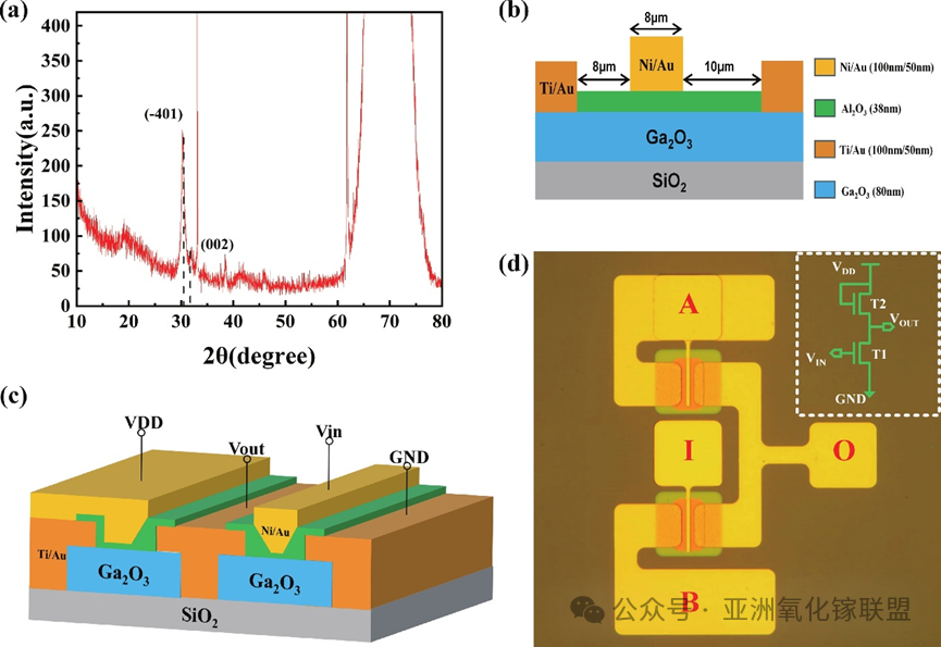
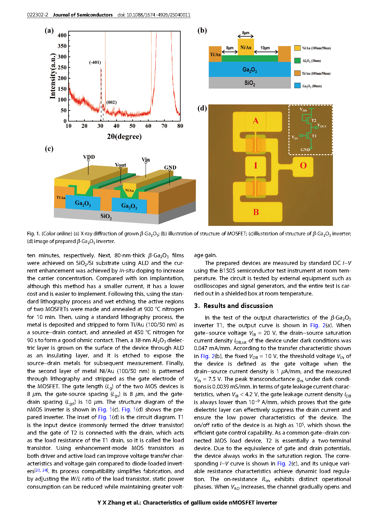
Fig. 1. (a) X-ray diffraction of grown β-Ga2O3; (b) illustration of structure of MOSFET; (c)illustration of structure of β-Ga2O3 inverter; (d) image of prepared β-Ga2O3 inverter.
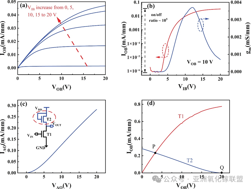
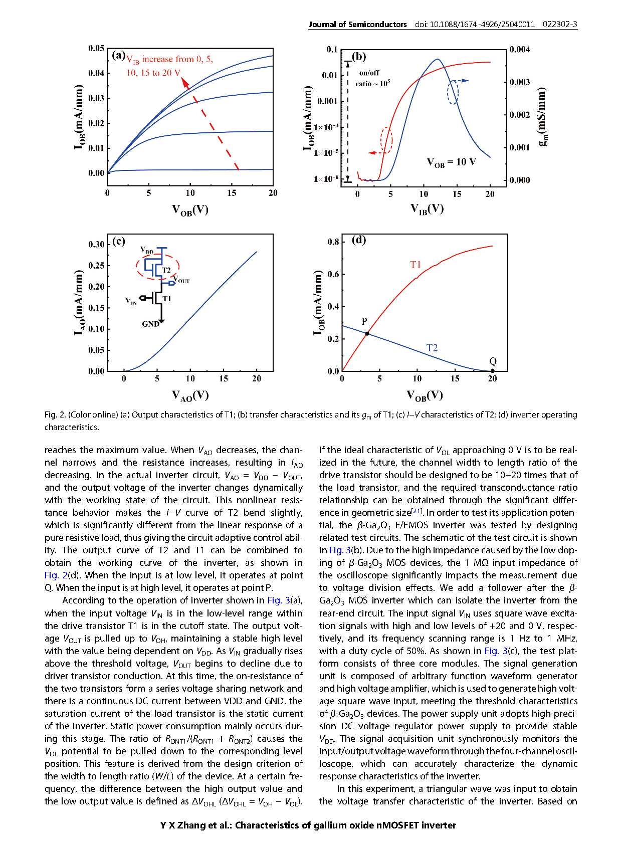
Fig. 2. (a) Output characteristics of T1; (b) transfer characteristics and its gm of T1; (c) I−V characteristics of T2; (d) inverter operating characteristics.
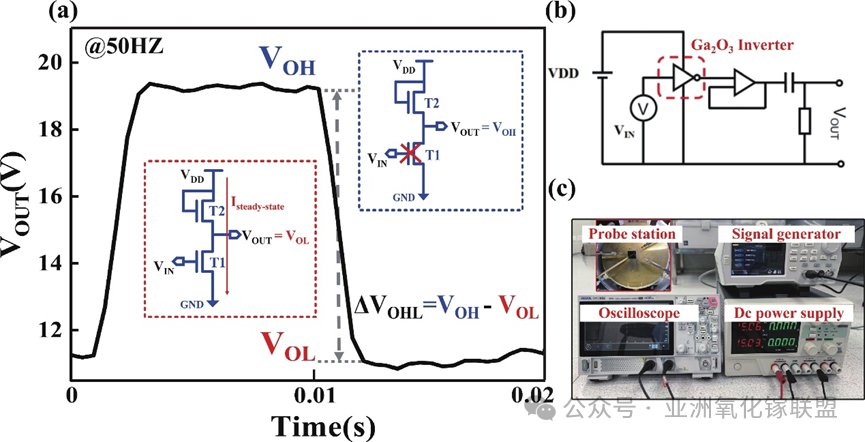
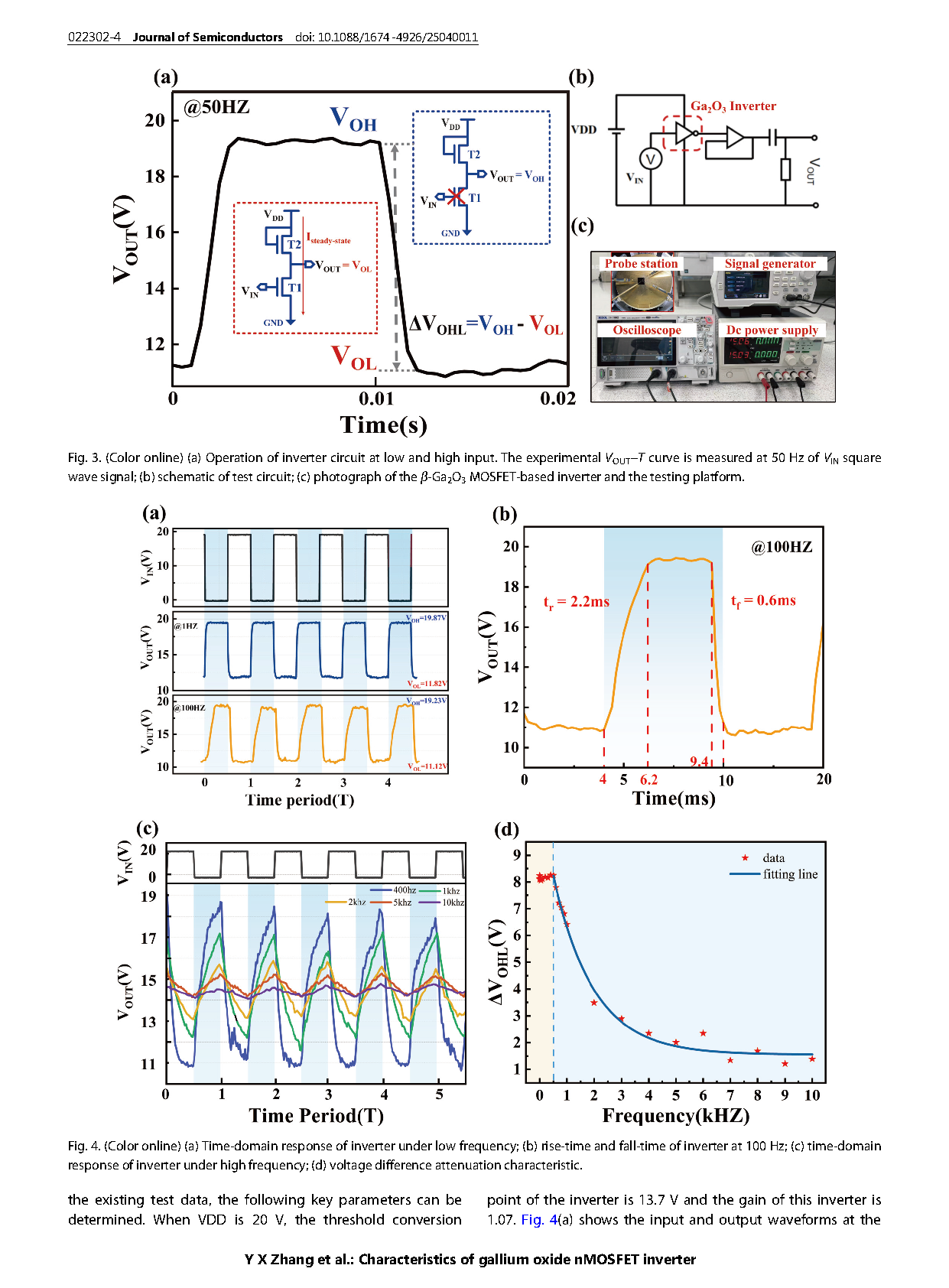
Fig. 3. (a) Operation of inverter circuit at low and high input. The experimental VOUT−T curve is measured at 50 Hz of VIN square wave signal; (b) schematic of test circuit; (c) photograph of the β-Ga2O3 MOSFET-based inverter and the testing platform.
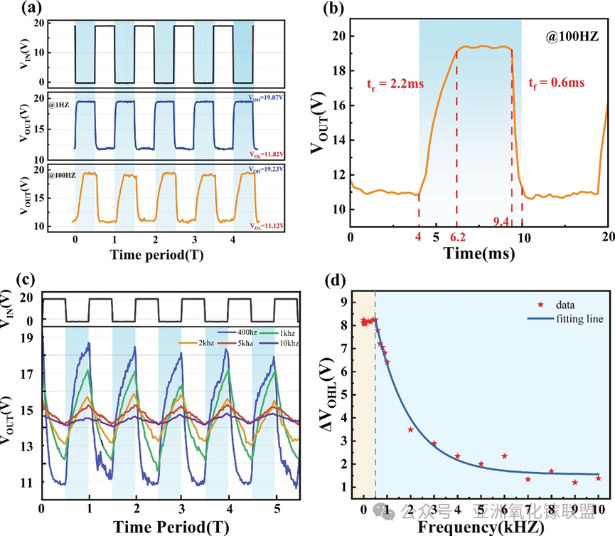
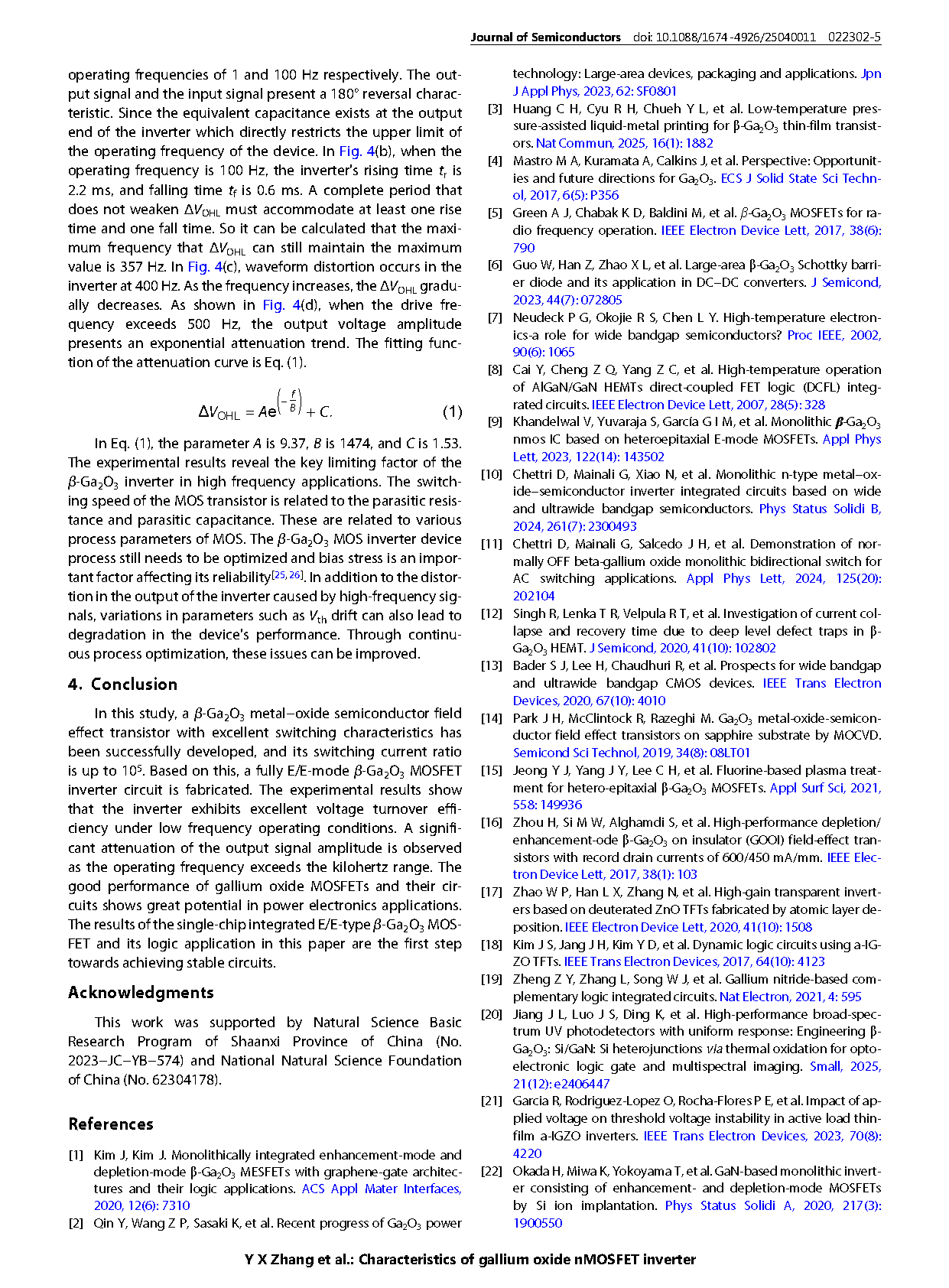
Fig. 4. (a) Time-domain response of inverter under low frequency; (b) rise-time and fall-time of inverter at 100 Hz; (c) time-domain response of inverter under high frequency; (d) voltage difference attenuation characteristic.
DOI:
doi.org/10.1088/1674-4926/25040011