Paper Sharing
【International Papers】On the nature of deep-level defects in β-Ga₂O₃ epilayers: The impact of isochronal rapid thermal annealing
日期:2026-03-24阅读:186
Researchers from the University of Manchester have published a dissertation titled "On the nature of deep-level defects in β-Ga2O3 epilayers: The impact of isochronal rapid thermal annealing" in Journal of Applied Physics.
Background
Monoclinic gallium oxide (β-Ga₂O₃) is a promising material for high-power and deep-ultraviolet optoelectronic devices. With an ultrawide bandgap of approximately 4.8 eV, it features a high theoretical breakdown field of 8 MV/cm and a superior Baliga figure of merit compared with mainstream wide bandgap semiconductors such as SiC and GaN. Large-area 6-in single crystals of β-Ga₂O₃ can be directly grown from the melt via the vertical-Bridgman method, enabling high-quality homoepitaxial growth and mitigating extended defects induced by foreign substrates. N-type conductivity of β-Ga₂O₃ can be finely controlled in the range of 1015~1020 cm⁻³ through doping with shallow donors like Si, Sn and Ge, while p-type conductivity is practically unfeasible due to the large distance between the vacuum level and the valence band maximum, as well as low hole mobility caused by the flat valence band.
High-performance unipolar β-Ga₂O₃ devices require epilayers with controllable free electron densities and low defect concentrations. However, the low symmetry of β-Ga₂O₃'s monoclinic crystalline structure leads to two inequivalent gallium sites, three oxygen sites, six interstitial sites and easy formation of split vacancies, resulting in multiple lattice sites for impurities, complex electronic properties and low formation energy of complex defects. This makes it difficult to identify the candidate defects of the E1 trap and conduct in-depth research on deep-level defects. Previous studies have not systematically analyzed the thermal stability and electric field dependence of defects in β-Ga₂O₃. In this work, conventional deep-level transient spectroscopy (DLTS) and high-resolution Laplace-DLTS were combined with isochronal rapid thermal annealing (RTA) at 150~450℃ in N₂ atmosphere to investigate deep-level defects in Si-doped (010) β-Ga₂O₃ epilayers grown by metal-organic chemical vapor deposition (MOCVD), providing support for defect control and device optimization of this material.
Abstract
Deep-level transient spectroscopy (DLTS) and Laplace-DLTS were used to investigate electrically active defects in (010)-oriented β-Ga₂O₃ epilayers grown via metal-organic chemical vapor deposition and doped with Si during growth. The impact of isochronal rapid thermal annealing in N₂ on the electrical characteristics of Pt Schottky barrier diodes and on defect concentrations was examined by annealing at temperatures from 150 to 450 °C with 100 °C increments. Four deep levels were detected, with concentrations in the range of 10¹³~10¹⁴ cm⁻³ and activation energies of electron emission to the conduction band (ΔEc) of 0.06, 0.40, 0.55, and 0.62 eV. The Ec-0.06 eV trap was no longer observed in DLTS measurements after heating to 400 K, and the Ec-0.62 eV trap was suppressed after annealing at 350 °C. In contrast, the Ec-0.40 eV trap progressively reduced in concentration, while the trap density of the Ec-0.55 eV level increased with each rapid thermal annealing step, suggesting defect redistribution along the [010] direction. The electric field dependence of the electron emission rates indicates acceptor-like behavior for the Ec-0.55 eV state and donor-like behavior for the Ec-0.62 eV state. As both states exhibit activation energies consistent with the commonly reported E1 defect, we propose the following labelling conventions: E1a (Ec-0.55 eV) and E1b (Ec-0.62 eV). The nature and potential origins for each of the observed defects are discussed.
Highlights
The effects of isochronal rapid thermal annealing at 150~450℃ in N₂ atmosphere on electrically active deep-level defects in Si-doped (010) β-Ga₂O₃ epilayers grown by MOCVD were systematically investigated, and the influence of annealing on the electrical characteristics of Pt Schottky barrier diodes was also analyzed.
Four well-characterized deep-level defects were detected in the target material, with their electron emission activation energies ranging from 0.06 to 0.62 eV and concentrations all in the range of 10¹³~10¹⁴ cm⁻³.
The differences in thermal stability of different deep-level defects were revealed: E10 (Ec-0.06 eV) disappears after 400 K, E1b (Ec-0.62 eV) is suppressed after annealing at 350℃, the concentration of E9 (Ec-0.40 eV) decreases continuously with annealing, and the trap density of E1a (Ec-0.55 eV) increases gradually with annealing, confirming the defect redistribution along the [010] direction.
Through the analysis of the electric field dependence of electron emission rate, E1a was identified as an acceptor-like defect and E1b as a donor-like defect. A detailed naming convention of E1a/E1b was proposed for the widely reported E1 defect for the first time, solving the problem of ambiguous characterization of the E1 defect.
The variation mechanism of carrier concentration in β-Ga₂O₃ epilayers during reverse-bias annealing and isochronal rapid thermal annealing, as well as its internal relationship with defect migration and activation, were clarified.
Conclusion
In conclusion, we have investigated Si-doped MOCVD-grown β-Ga₂O₃ using DLTS and Laplace-DLTS to characterize the relative thermal stability and electric-field-dependent donor-like and acceptor-like behavior of electrically active defects. The results indicate that traps at Ec-0.06 eV (E10) and Ec-0.62 eV (E1b) are donor levels, whereas traps at Ec-0.40 eV (E9) and Ec-0.55 eV (E1a) are deep acceptors. The effect of reverse-bias annealing induced during DLTS measurements and isochronal rapid thermal annealing on the apparent trap density was also used to explore the relative thermal stabilities and migration behavior of the defects. The findings suggest instability or out-diffusion from the epilayer for E9 and E1b, as well as thermally activated generation or in-diffusion into the epilayer for E1a. In contrast, for E10, the rapid decrease in the apparent trap density is attributed to electric field enhanced electron emission as dopants became thermally activated with successive annealing steps. Interestingly, previous work by our group did not indicate that E1a is generated following RTA, and therefore, the specific sequence in which the experimental procedures were applied in this present study may play a critical role in the formation of E1a and the concurrent suppression of E9. The combined analysis of activation energies, donor/acceptor behavior, and relative thermal stability strongly suggests that traps reported near Ec-0.60 eV in previous publications, and commonly assigned as E1, are in fact closely spaced defect states within the bandgap. Accordingly, the distinct designations E1a and E1b for deep levels observed at Ec-0.55 eV and Ec-0.62 eV, respectively, are proposed, which can be unambiguously differentiated through analysis of their donor-like and acceptor-like nature.
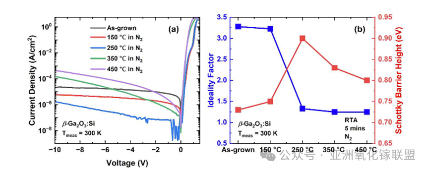
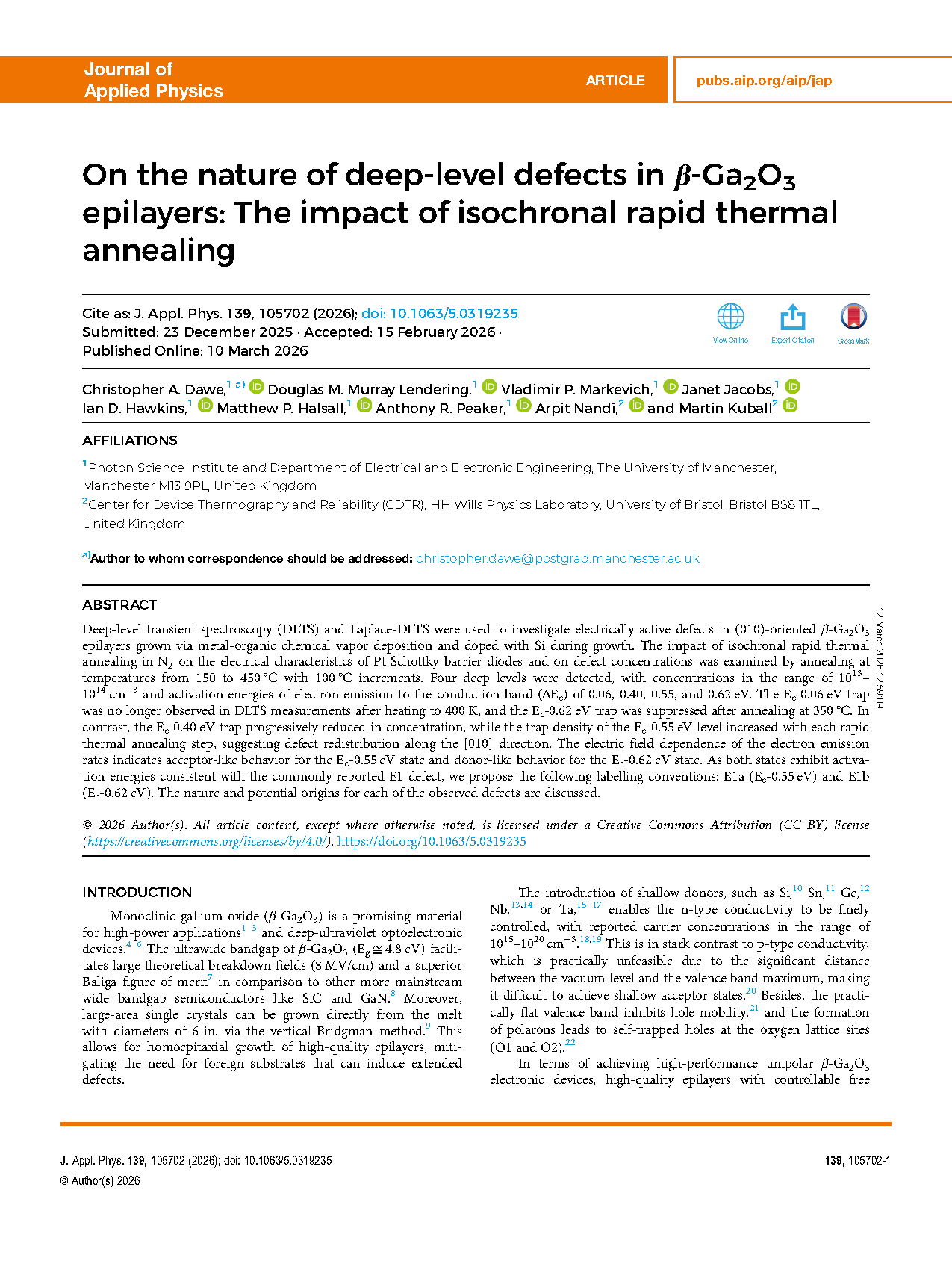
FIG. 1. (a) Current density–voltage (J–V) dependencies for the Pt/β-Ga2O3 Schottky diodes, measured at 300 K, for the sample in the as-grown state as well as after each rapid thermal treatment in the temperature range of 150–450 °C. (b) Ideality factor and Schottky barrier height as a function of anneal temperature in N2, derived from the thermionic emission model.
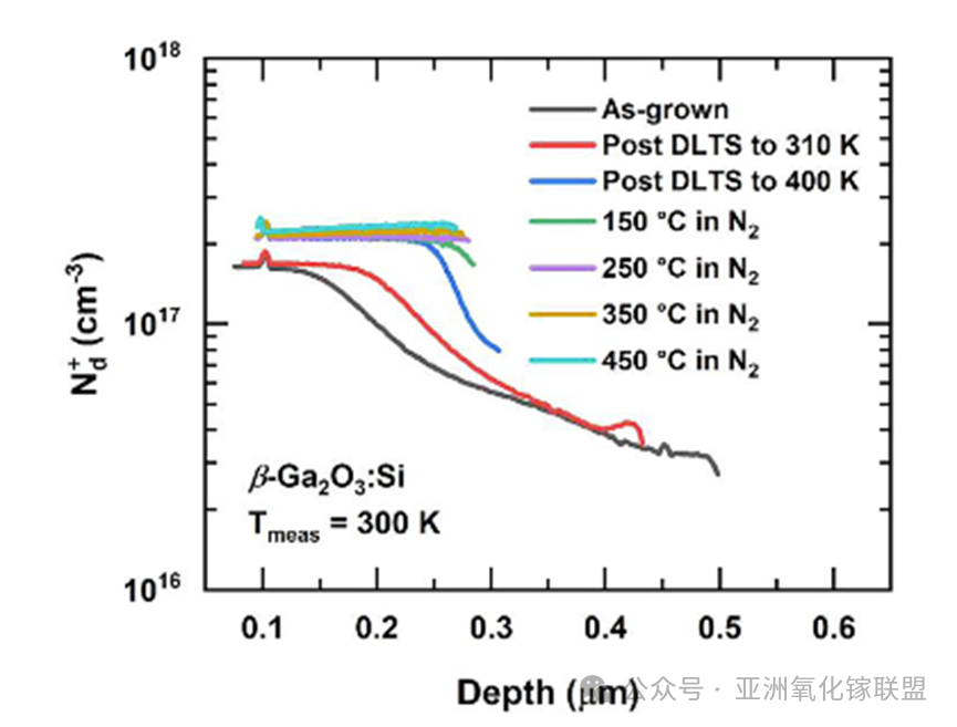
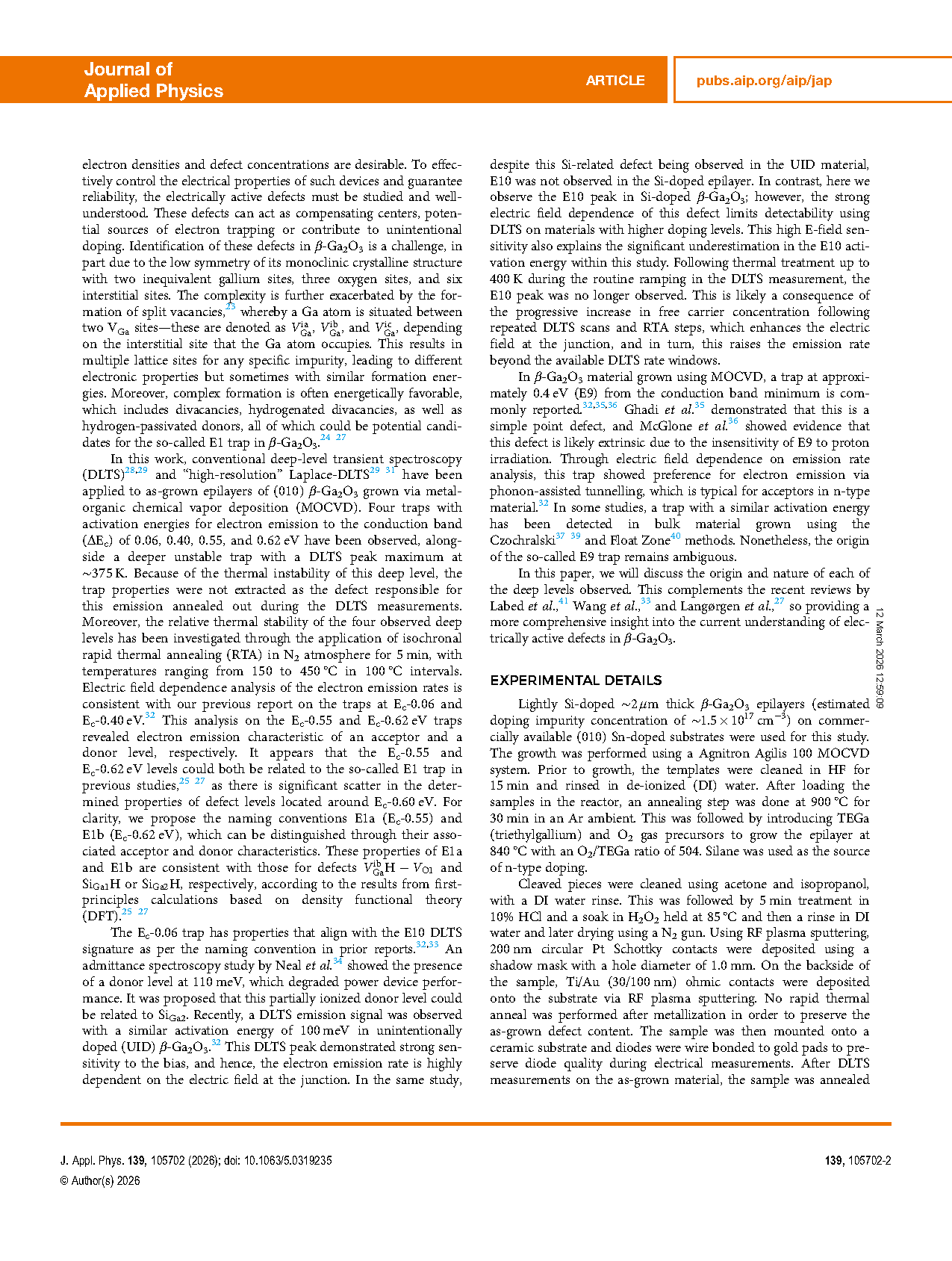
FIG. 2. Depletion depth profiles for the concentration of uncompensated ionized donors for the Pt/β-Ga2O3 Schottky diodes, as derived from C–V measurements at 300 K. Depth profiles derived from pre- and post-DLTS scans are presented, as well as those obtained after each subsequent isochronal rapid thermal anneal in N2.
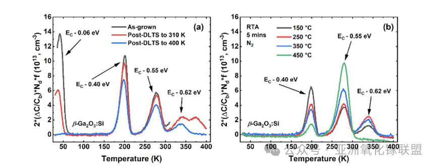
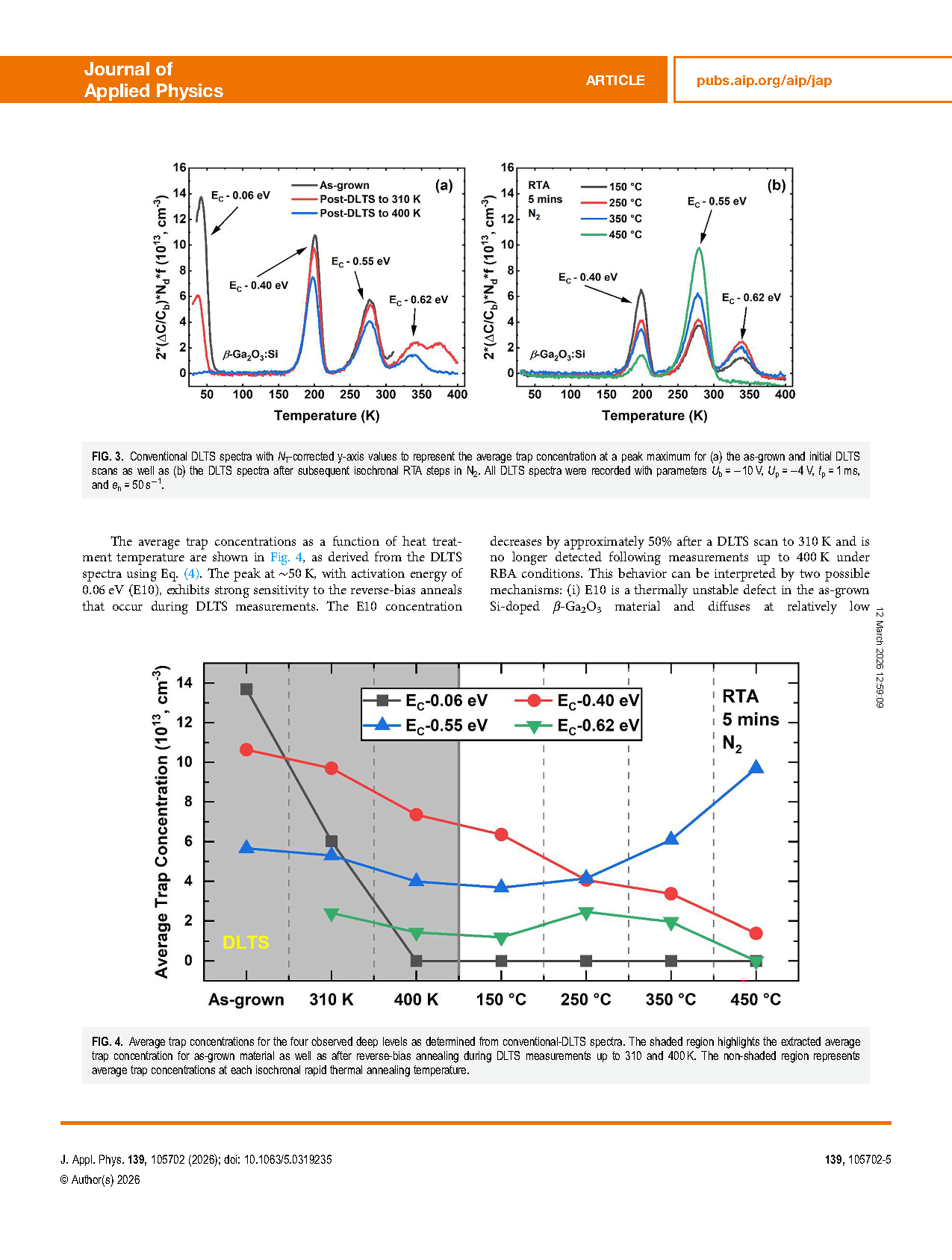
FIG. 3. Conventional DLTS spectra with NT-corrected y-axis values to represent the average trap concentration at a peak maximum for (a) the as-grown and initial DLTS scans as well as (b) the DLTS spectra after subsequent isochronal RTA steps in N2. All DLTS spectra were recorded with parameters Ub =-10 V, Up=-4 V, tp = 1 ms, and en = 50 s−1.
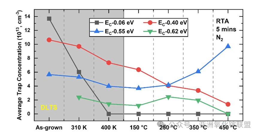
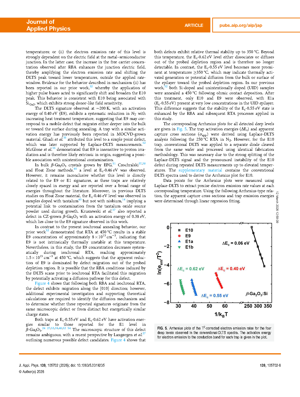
FIG. 4. Average trap concentrations for the four observed deep levels as determined from conventional-DLTS spectra. The shaded region highlights the extracted average trap concentration for as-grown material as well as after reverse-bias annealing during DLTS measurements up to 310 and 400 K. The non-shaded region represents average trap concentrations at each isochronal rapid thermal annealing temperature.
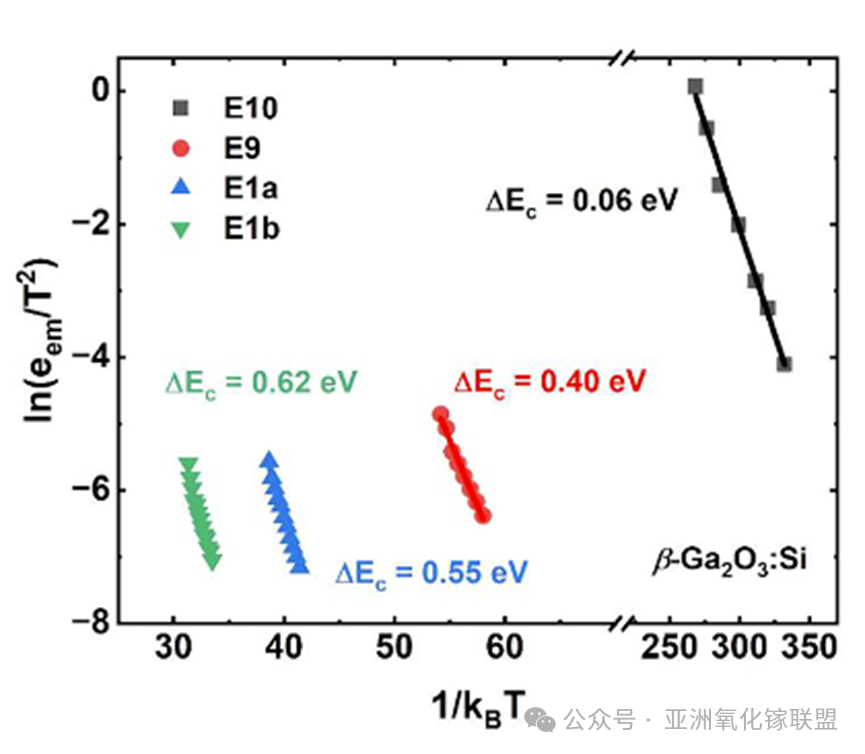
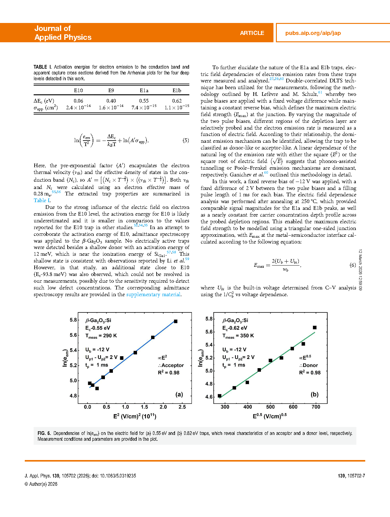
FIG. 5. Arrhenius plots of the T2-corrected electron emission rates for the four deep levels observed in the conventional-DLTS spectra. The activation energy for electron emission to the conduction band for each trap is given in the plot.
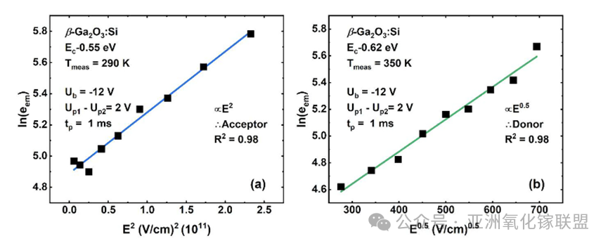
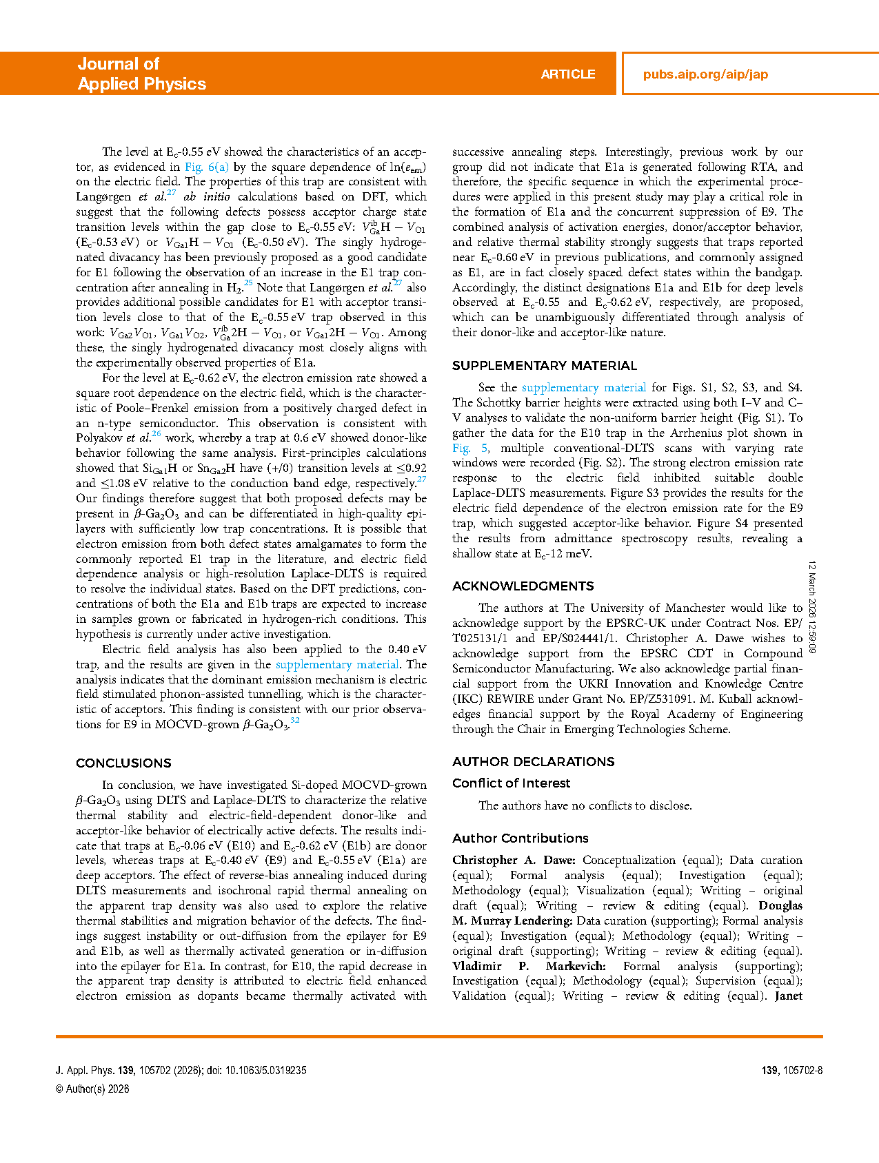
FIG. 6. Dependencies of ln(eem) on the electric field for (a) 0.55 eV and (b) 0.62 eV traps, which reveal characteristics of an acceptor and a donor level, respectively. Measurement conditions and parameters are provided in the plot.
DOI:
doi.org/10.1063/5.0319235