Paper Sharing
【Domestic Papers】TCAD-Based Investigation of a-GaOx UV Phototransistors
日期:2026-03-24阅读:196
Researchers from the Ningbo Institute of Materials Technology and Engineering, Chinese Academy of Sciences have published a dissertation titled " TCAD-Based Investigation of a-GaOx UV Phototransistors" in Coatings.
Project Support
The authors acknowledge the help of Meng Xu in Shanghai University, for the construction of device models in TCAD simulations.
Background
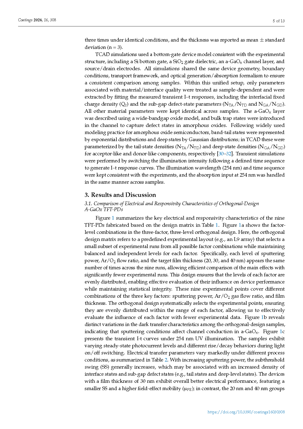
Ultraviolet (UV) detection technologies are important for applications such as environmental monitoring, space exploration, and secure communications. The solar-blind band (200–280 nm) has a very low terrestrial background because atmospheric ozone strongly absorbs these wavelengths, which supports low-noise UV detection with a high signal-to-noise ratio. Among solar-blind UV detector architectures, thin-film transistor photodetectors (TFT-PDs) integrate photodetection with gate-controlled amplification, enabling tunable responsivity magnitude and the operating window through gate bias, while also offering advantages in low power consumption and straightforward array-level integration. Amorphous gallium oxide (a-GaOx) exhibits a wide intrinsic bandgap, which enables a-GaOx TFT-PDs to achieve inherently low dark current and high UV sensitivity, making it an attractive channel material for solar-blind UV photodetectors. However, a-GaOx films are typically fabricated by low-thermal-budget processes like magnetron sputtering, where deposition parameters (e.g., sputtering power, Ar/O2 gas flow ratio, and thickness) affect film densification, oxygen-related defects, and interface charge states, which ultimately determine the device performance, including dark current, responsivity amplitude, and transient response. Thus, an efficient experimental design is needed to optimize these key parameters and identify the primary causes of performance variation.
Abstract
Amorphous gallium oxide thin-film transistor photodetectors are promising for ultraviolet detection because of their wide bandgap and low dark current. Magnetron sputtering is compatible with low-temperature processing, but device performance is sensitive to sputtering conditions. Poor parameter choices can introduce oxygen vacancies and interface charges, degrading optoelectronic performance. Here, a three-factor, three-level orthogonal design is used to vary sputtering power, Ar/O2 flow ratio, and film thickness. Nine device sets are fabricated and compared based on transfer characteristics and transient photocurrent–time (I-t) responses measured at a wavelength of 254 nm, with clear differences observed among process combinations. To identify the origin of these differences, representative samples with significant responsivity variations were modeled using TCAD. By fitting the simulated I-t curves to measured transients, the interface fixed charge density and defect-state densities were extracted, and the photon absorption distribution of different samples was analyzed. This analysis, from both defect and UV absorption perspectives, revealed the reasons for the differences in responsivity. The absorption coefficients at 254 nm measured by ellipsometry for the two samples were also compared, and the absorption trends observed in both the simulation and ellipsometry were consistent, confirming the accuracy of the simulation results. This work presents an integrated experimental and TCAD approach for process optimization and mechanistic analysis of a-GaOx TFT-PDs.
Conclusions
This work mainly investigates the sputtering parameters on the optoelectronic performance of bottom-gate a-GaOx TFT-PDs using a three-factor, three-level orthogonal design. We evaluate the coupled roles of sputtering power, Ar/O2 flow ratio, and film thickness on the device performance based on the transfer curves and 254 nm I-t responses. Different parameter combinations lead to dramatic variations in transfer behavior and transient response, which affect photocurrent, photo/dark current ratio, and responsivity. Interface fixed charge density and trap-state parameters (tail and deep levels) are extracted based on TCAD simulation under the same experimental conditions, and these parameters are found to be highly dependent on the deposition conditions. The simulated photon absorption-rate profile closely matches the ellipsometry-derived absorption coefficients at 254 nm, confirming the presence of absorption differences. Together, the extracted trap parameters and absorption profile not only explain the responsivity differences across devices but also provide direct support for process optimization. This combined experimental–TCAD workflow is not limited to a-GaOx TFT photodetectors. It can be easily extended to other oxide-based TFT-PD systems, such as IGZO, ZnO, In2O3, or SnO2-based channels, where device performance is governed by similar factors, including process-dependent defect states, interfacial charge, and optical absorption. By combining orthogonal process screening with transient-response fitting and internal-physics analysis in TCAD, this approach offers a general framework to extract comparable defect/charge parameters and identify performance-limiting factors for optimization across a wide range of oxide-based photodetectors.
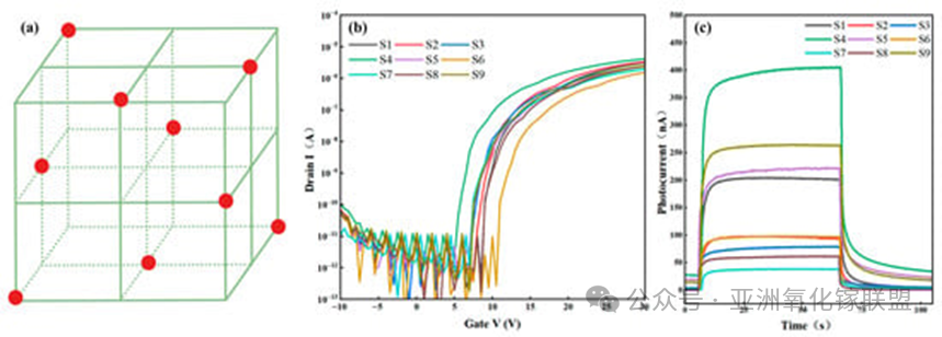
Figure 1. Orthogonal design matrix and the corresponding electrical and responsivity characteristics. (a) Factor-level combinations in the three-factor, three-level orthogonal design; (b) dark transfer curves of the a-GaOx TFT-PDs; (c) transient I-t curves measured under 254 nm illumination (power density: 0.741 µW∙cm−2) at VDS = 10.1 V. During the transient measurement, VGS is fixed at the turn-on voltage (VON) extracted from the dark transfer curve of each device.
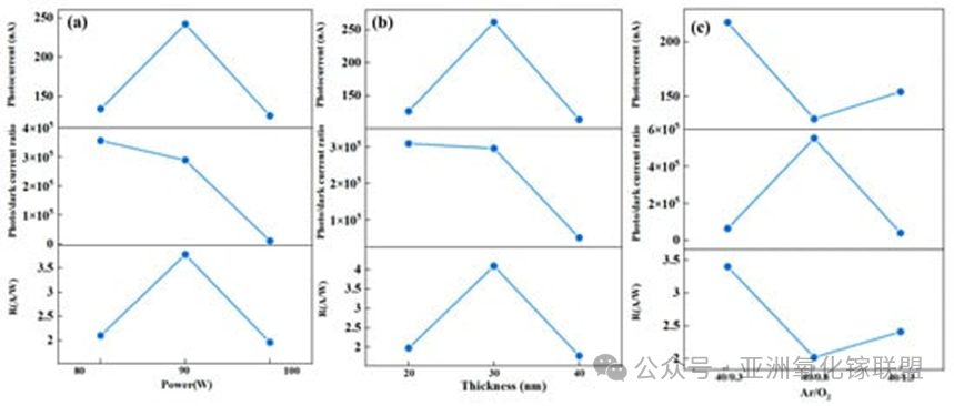
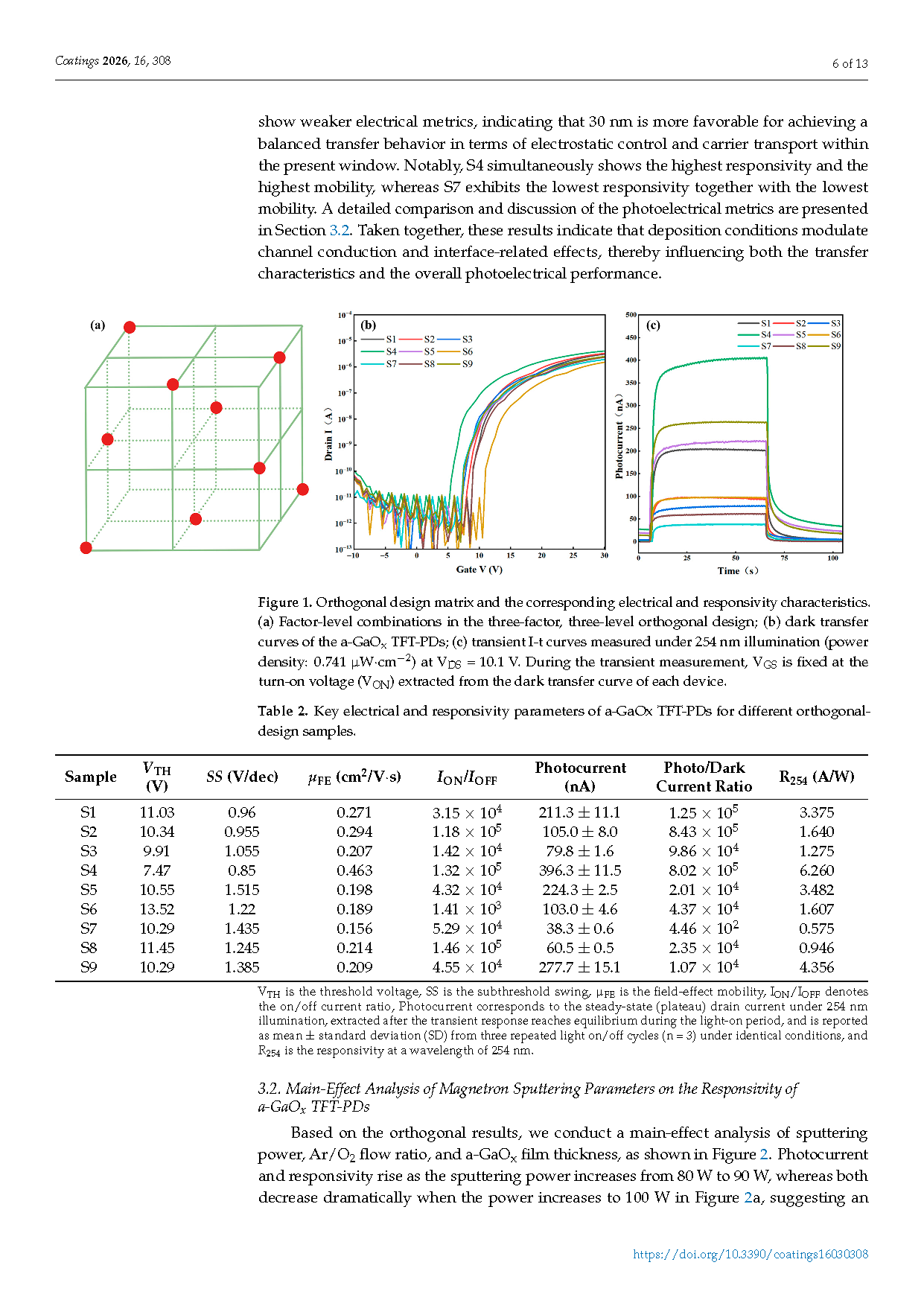
Figure 2. Main-effect analysis of magnetron sputtering parameters on the responsivity of a-GaOx TFT-PDs. (a) Sputtering power; (b) a-GaOx film thickness; (c) Ar/O2 flow ratio. From top to bottom, the metrics are photocurrent, photo/dark current ratio, and responsivity.
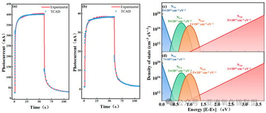
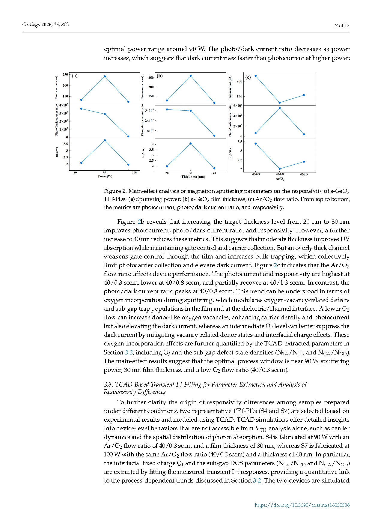
Figure 3. TCAD fitting and defect-parameter extraction for representative devices with distinct responsivity. The I-t curves are measured and simulated under 254 nm illumination with a power density of 0.741 µW∙cm−2 at VDS = 10.1 V; the bias settings are consistent with the experiment, and VGS is fixed at VON defined from the dark transfer curve. (a) Experimental and TCAD-simulated I-t curves of S4 under 254 nm UV illumination; (b) experimental and TCAD-simulated I-t curves of S7 under 254 nm UV illumination; (c) extracted defect-state density of states (DOS) for S4 used in the TCAD fitting; (d) extracted defect-state DOS for S7 used in the TCAD fitting.
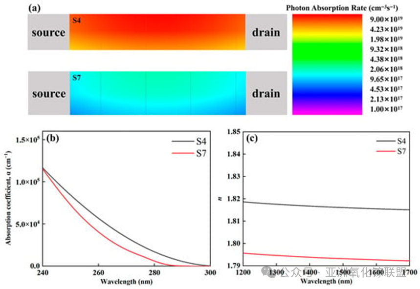
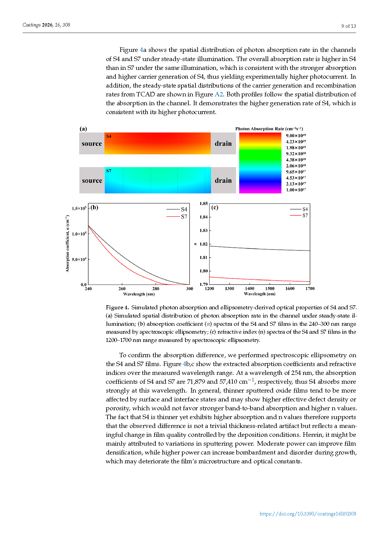
Figure 4. Simulated photon absorption and ellipsometry-derived optical properties of S4 and S7. (a) Simulated spatial distribution of photon absorption rate in the channel under steady-state illumination; (b) absorption coefficient (α) spectra of the S4 and S7 films in the 240–300 nm range measured by spectroscopic ellipsometry; (c) refractive index (n) spectra of the S4 and S7 films in the 1200–1700 nm range measured by spectroscopic ellipsometry.
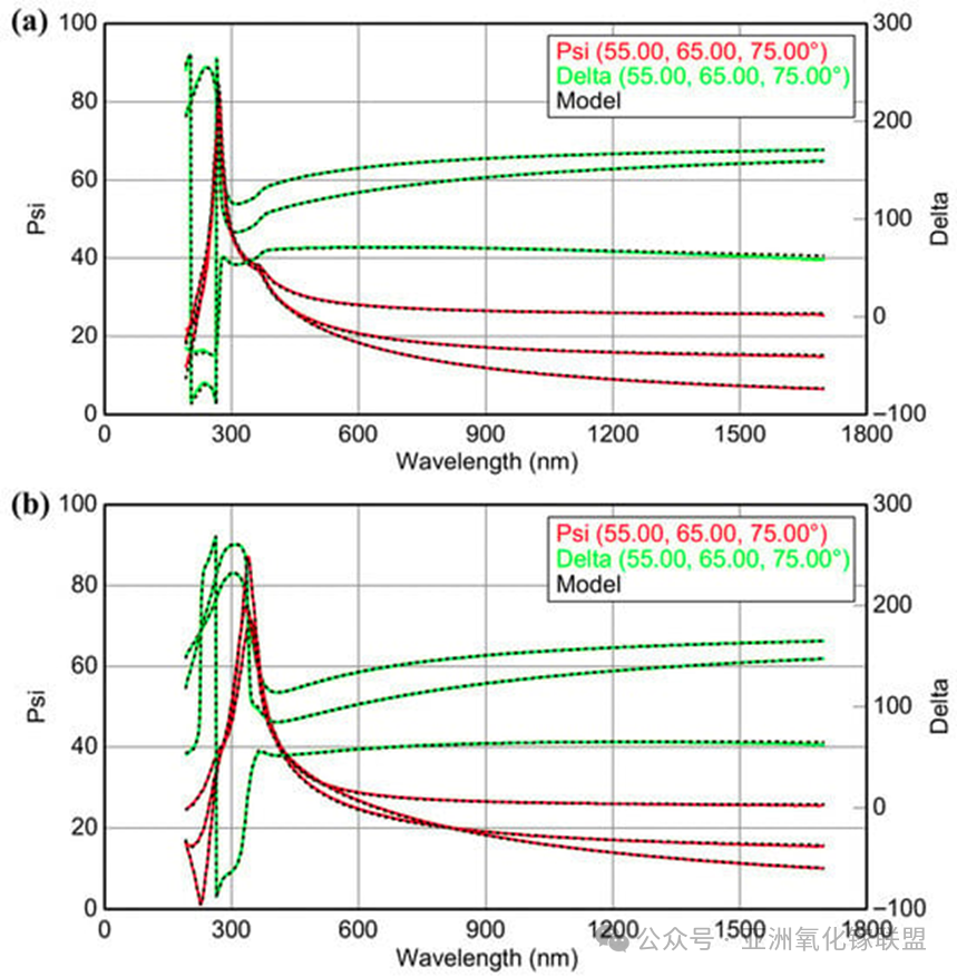
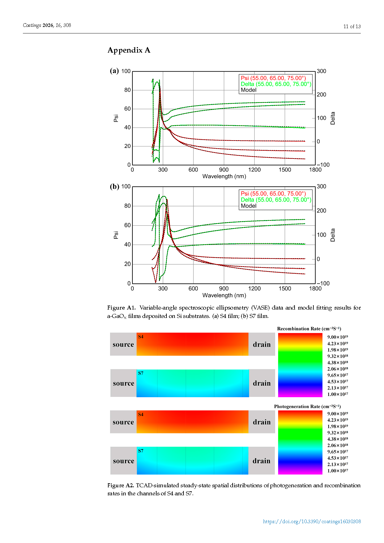
Figure A1. Variable-angle spectroscopic ellipsometry (VASE) data and model fitting results for a-GaOx films deposited on Si substrates. (a) S4 film; (b) S7 film.
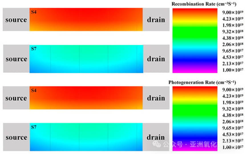
Figure A2. TCAD-simulated steady-state spatial distributions of photogeneration and recombination rates in the channels of S4 and S7.
DOI:
doi.org/10.3390/coatings16030308