


Member News
【Member News】At APCSCRM 2025, Spotlight on Semianaly Semiconductor ’s Technologies and Products
日期:2025-12-14阅读:447
At the 6th Asia Pacific Conference on Silicon Carbide and Related Materials (APCSCRM 2025), Gallium Oxide emerged as one of the most prominent focal points in the field. As an invited participant, the Asian Gallium Oxide Alliance (AGOA) conducted an interview with its council member—Semianaly Semiconductor—during the conference. In the following section, we take a closer look at Raphael Optech, its core businesses, and its flagship products as presented.
Semianaly Semiconductor

Founded in 2021 and based in Suzhou, Semianaly Semiconductor is a manufacturer of world-leading non-contact semiconductor testing and analysis equipment. The company integrates R&D, design, manufacturing, and sales, focusing on overcoming foreign monopoly technologies and replacing imported products to achieve localization of semiconductor material testing equipment. Semianaly has filed over 50 intellectual property rights and, leveraging its advanced technologies and comprehensive product line, has become one of the few Chinese mainland providers of specialized semiconductor equipment with international competitiveness. Its products are recognized by numerous leading domestic and international semiconductor manufacturers and have earned an excellent market reputation.
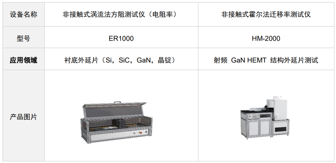
Semianaly Semiconductor offers a well-rounded product portfolio covering key testing processes, including eddy current resistivity testers, non-contact square resistance testers, non-contact Hall mobility testers, minority carrier lifetime testers, PN-type testers, and semi-insulating SiC high-resistance testers. The products excel in stability, accuracy, and durability, while the company continuously drives technological iteration—minority carrier lifetime testers have already been successfully deployed, and semi-insulating SiC high-resistance testers and ECV epitaxial testing equipment are actively under development.
In terms of delivery capability, Semianaly demonstrates significant supply chain advantages, with lead times as short as 2–4 weeks and a maximum of 6–8 weeks—far shorter than the 6–12 months typical of foreign competitors—and can customize equipment for any wafer size, effectively supporting clients’ R&D and production schedules.
Key Advantages
● Global leader in non-contact electrical semiconductor manufacturing equipment;
● SiC resistivity equipment: since 2021, the company’s third-generation products have achieved over 90% market share;
● Equipment compatible with 4–12 inch wafers, capable of testing up to 350 mm;
● Proprietary core IP with customizable functions;
● Ingot-to-wafer integrated testing: simultaneous testing of ingots and wafers.
For more information
Contact: Zhang Zhanwu
Phone: +86 13739170031
Email: zhang9602@126.com
Website: www.analysemi.com
