


Member News
【Member News】New Product Release: GAREN SEMI “SCIENCE Series” Research-Grade VB Crystal Growth Equipment
日期:2025-12-14阅读:431
Amid the rapid growth of the fourth-generation semiconductor industry, Gallium Oxide, as a core ultrawide-bandgap semiconductor material, is becoming a key focus of research efforts in universities and research institutes.
To address long-standing challenges in research-stage crystal growth equipment—such as narrow adaptability, insufficient precision, and complex operation—Hangzhou Garen Semiconductor Co., Ltd. officially launches its new product: the “SCIENCE Series” research-grade VB crystal growth system. Tailored specifically for 2–6 inch Gallium Oxide research scenarios, this system leverages fully in-house core technologies to support researchers in efficiently exploring crystal growth, doping, defect control, and material property optimization.
The “SCIENCE Series” research-grade VB crystal growth system is now open for pre-orders. Universities and research institutions are warmly invited to collaborate with us to jointly explore the application potential of gallium oxide and create new value for the semiconductor industry.
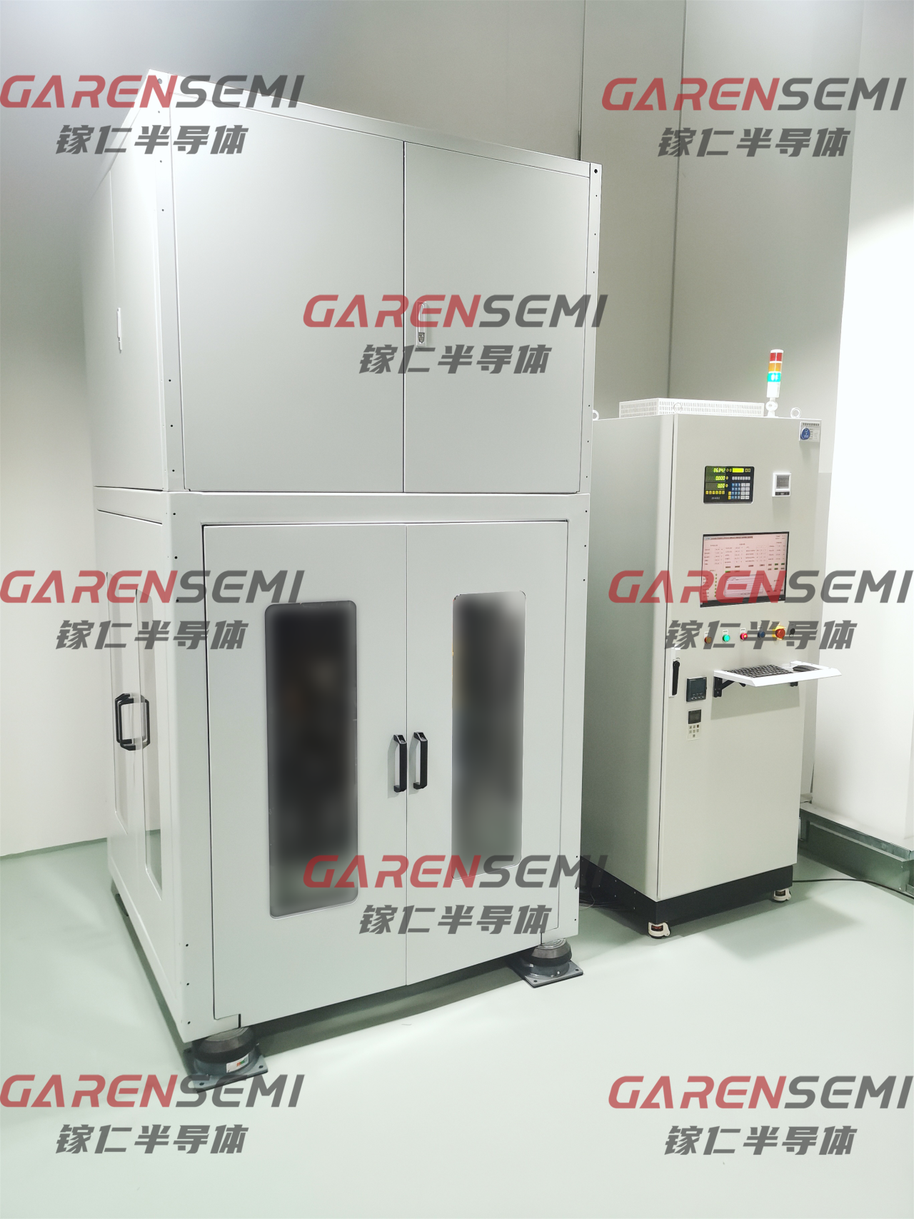
Research-Grade Configuration Unlocking Unlimited Research Potential
Built upon Garen Semiconductor’s years of technological accumulation in Gallium Oxide industrialization, the “SCIENCE Series” achieves triple breakthroughs in stability, precision, and compatibility—making it a reliable partner throughout the research journey.
01 Wide Size Compatibility Covering Diverse Needs
Flexibly supports 2-inch, 4-inch, and 6-inch Gallium Oxide single-crystal growth using the VB method, without the need for frequent replacement of core components. This enables seamless coverage from fundamental research to pilot-scale studies, significantly reducing equipment investment costs for research institutions.
02 Precision Control of Critical Parameters
Equipped with a self-developed fully automated composite temperature measurement technology and control algorithms, achieving temperature control accuracy of ±0.1 °C. This ensures stability, uniformity, and consistency during crystal growth, markedly improving growth efficiency and crystal quality, and enabling in-depth investigation of correlations between material properties and process parameters.
03 Stable and Reliable Operation Ensuring Experimental Continuity
Featuring a visualized operation interface and intelligent data logging functions, the system enables real-time monitoring of key growth parameters, reduces manual errors, and accelerates research progress. Outstanding long-term operational stability provides solid support for extended experimental campaigns.
Strong Track Record Demonstrating Hard-Core Capabilities
The launch of this new equipment is grounded in Garen Semiconductor’s continuous technological breakthroughs in the Gallium Oxide field. Leveraging its self-developed VB equipment and processes, the company has already realized scalable production of 6-inch Gallium Oxide crystals and epitaxial wafers, providing mature technical validation for research-grade systems.
In VB-grown gallium oxide single-crystal development, Garen Semiconductor achieved a leap from 2-inch to 6-inch crystals within just one year. The VB-grown 6-inch (010)-oriented Gallium Oxide ingots exhibit equal-diameter section lengths exceeding 40 mm, high phase purity, low defect density, and crystal quality reaching internationally leading levels—providing high-quality base materials for downstream epitaxial growth.
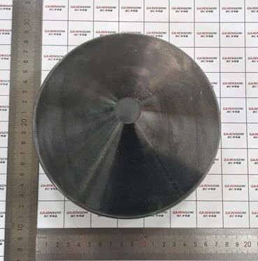
Garen Semiconductor VB-grown 6-inch (010) Gallium Oxide bulk (conductive type)
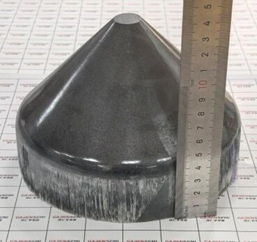
Equal-diameter section length of VB-grown 6-inch (010) Gallium Oxide bulk
Breakthroughs in Homoepitaxy
In the field of Gallium Oxide homoepitaxy, the company has successfully achieved 6-inch Gallium Oxide homoepitaxial growth based on its own gallium oxide substrates. Characterization results show low defect density, excellent thickness uniformity and crystallinity, good controllability and consistency, as well as suitable electrical properties—effectively addressing lattice mismatch issues inherent to traditional heteroepitaxy.
This achievement not only provides a new solution for high-voltage power device fabrication, but also validates the superior performance of single-crystal substrates grown using the “SCIENCE Series” equipment.
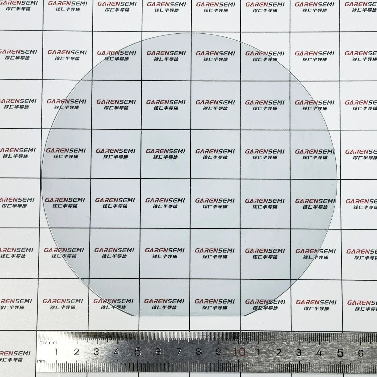
Garen Semiconductor 6-inch Gallium Oxide homoepitaxial wafer
About Garen Semiconductor
Hangzhou Garen Semiconductor Co., Ltd. is a globally leading provider of Gallium Oxide materials and equipment solutions, dedicated to the R&D and industrialization of ultrawide-bandgap semiconductors. Its core products include 2–8 inch gallium oxide single crystals and substrates (with 8-inch being a world first), Gallium Oxide vertical Bridgman (VB) crystal growth equipment, and Gallium Oxide epitaxial wafers. The company is committed to building a full-chain product system covering “equipment–crystal–substrate–epitaxy”, delivering comprehensive solutions to customers worldwide.
Garen Semiconductor’s achievements in Gallium Oxide have been featured by major media outlets including People’s Daily, Xinhua News Agency, Science and Technology Daily, Sina Finance, China Blue News, and The Paper.
Summary of Corporate Honors:In 2023, the company was recognized as a National High-Tech Small and Medium-Sized Enterprise and a Zhejiang Innovative SME; in 2024, it was awarded the title of Zhejiang “Specialized, Sophisticated, Distinctive, and Innovative” SME. In 2025, the company received multiple prestigious honors, including the SEMICON CHINA SEMI Sustainability Outstanding Contribution Award, the Synergy Award at the Jiufengshan Forum (JFSC) and Compound Semiconductor Industry Expo, the Innovation Vitality Award from the Zhejiang Semiconductor Industry, second prize in the enterprise category of the 10th “Maker China” Zhejiang Provincial Finals, a Top 500 ranking in the national enterprise category of the 10th “Maker China” SME Innovation and Entrepreneurship Competition, and the 2024–2025 Semiconductor Materials Industry Contribution Award. Its achievement titled “Major Breakthrough in the Preparation of 8-inch Gallium Oxide Single Crystals and Substrates” was selected as one of the Top Ten Advances in China’s Third-Generation Semiconductor Technology in 2025 and as a 2025 Major Scientific and Technological Achievement by the Zhejiang Provincial Department of Science and Technology. In addition, the company has led the drafting of two group standard proposals in the gallium oxide field, participated in the drafting of one national standard, and contributed to the promotion of another group standard proposal; it has received support from the “5213” Excellence Program of Xiaoshan District, Hangzhou; and it holds 13 granted invention patents in China and abroad (including in the United States and Japan), with more than 50 patent applications filed.
For more information about GAREN SEMI and its products
Visit our official website: http://garen.cc/
Or contact us in the following ways:
Mr. Jiang :15918719807
Email :jiangjiwei@garen.cc
Mr. Xia :19011278792
Email :xianing@garen.cc
