Paper Sharing
【Member Papers】High-performance DUV-visible dual-band photodetector enabled by β-Ga₂O₃/Au/Cs₂AgBiBr₆ heterojunction with sandwich architecture
日期:2025-12-11阅读:406
Researchers from the Northeast Normal University have published a dissertation titled "High-performance DUV-visible dual-band photodetector enabled by β-Ga2O3/Au/Cs2AgBiBr6 heterojunction with sandwich architecture" in Materials Today Physics.
Project Support
This work was supported by the National Key R&D Program of China (2021YFA0716404), the funding from Jilin Province (No. 20220502002GH), the National Natural Science Foundation of China (No. 52302166, No. 62404038, No. 12474164), the Science Technology Program of Jilin Province (20240602060RC), the National Postdoctoral Program for Innovative Talents (BX20230064), the Fundamental Research Funds for the Central Universities (No. 2412023QD004, No. 2412024QD009), the funding from Education Department of Jilin Province (JJKH20241412KJ), the Research Projects of the Education Office of Jilin Province (JJKH20250300KJ), Jilin Province Development and Reform Commission (2022C040-1), the Postdoctoral Fellowship Program of CPSF (GZC20240240).
Background
Dual-band photodetectors (PDs) covering the range from DUV to visible light regions are pivotal for optical communications, environmental monitoring, and sensing imaging. While silicon, transition metal dichalcogenides, and black phosphorus have been extensively explored for dual-band photodetection, these materials typically operate in the visible and near-infrared regions, with a weak response in the DUV region. To enable efficient DUV detection within dual-band PDs, ultra-wide bandgap semiconductors, such as MgxZn1-xO, AlxGa1-xN, diamond, BN, and β-Ga2O3 have been utilized as the DUV absorbing layers. Among these, β-Ga2O3 has gained prominence due to its direct bandgap (Eg ≈ 4.9 eV) and superior thermal/chemical stability.
Abstract
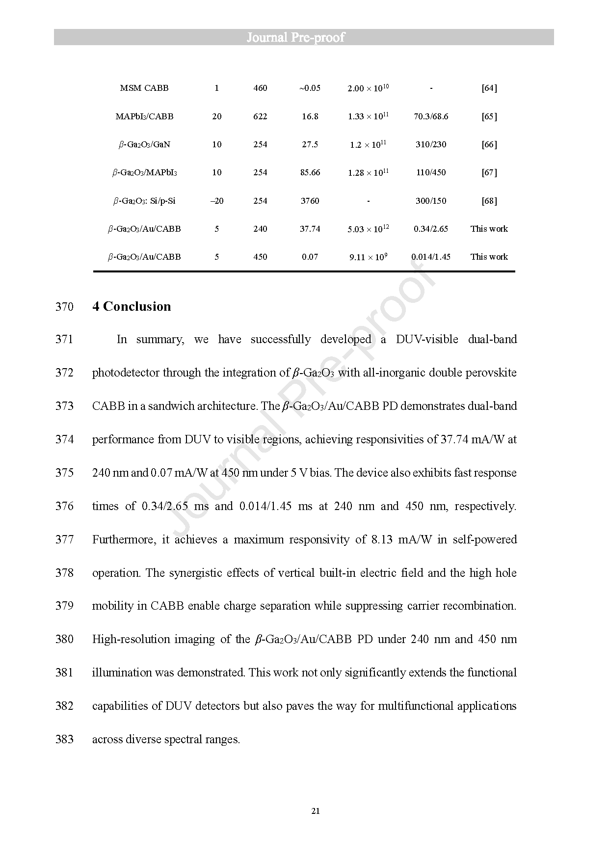
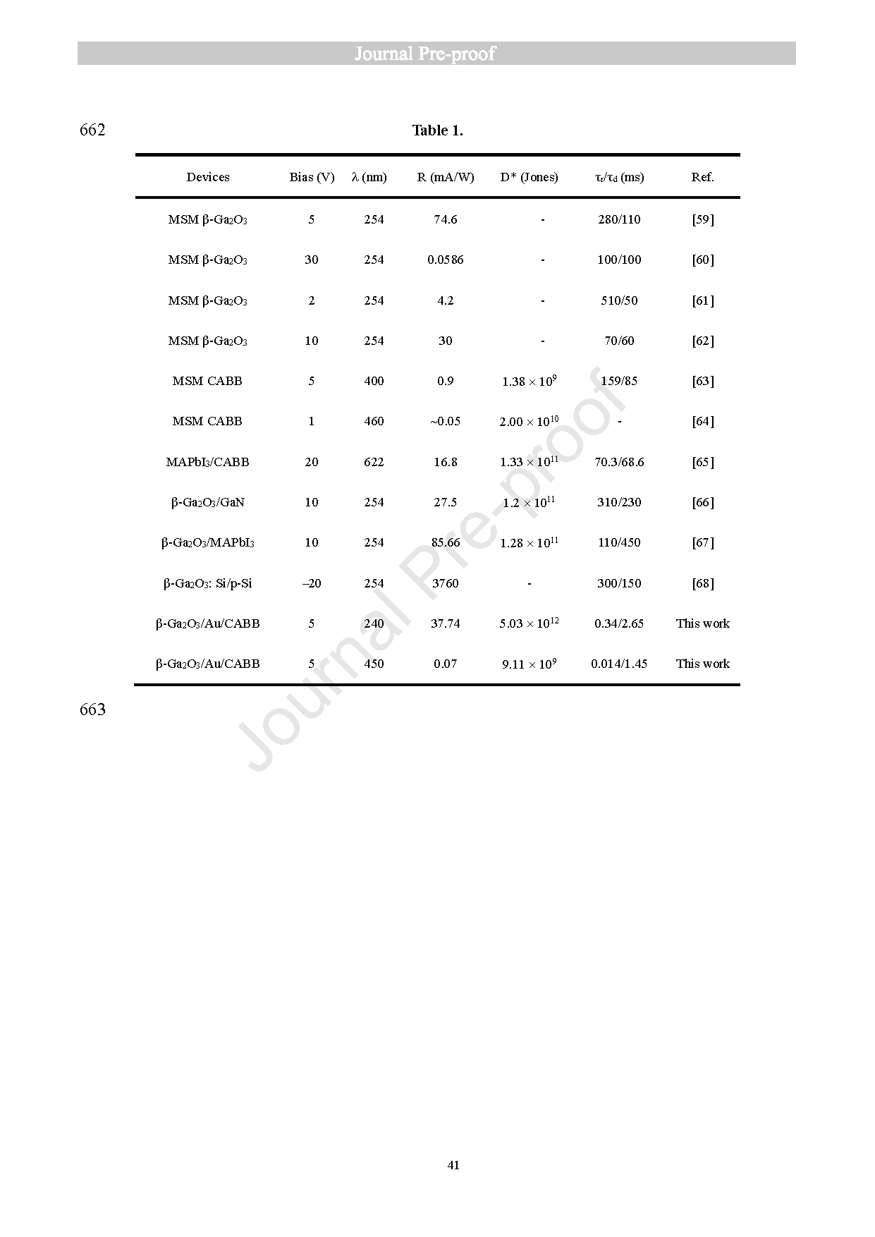
High sensitivity and fast response dual-band photodetectors (PDs) covering the deep-ultraviolet (DUV) to visible spectrum are highly desired for industrial and scientific applications. Herein, a sandwich-architecture PD covering the range from DUV to visible was prepared by stacking a β-Ga2O3 DUV absorbing layer, interdigitated Au electrodes, and a Cs2AgBiBr6 (CABB) visible absorbing layer. At 5 V bias voltage, the sandwich-architecture PD achieves responsivities of 37.74 mA/W at 240 nm and 0.07 mA/W at 450 nm with microsecond response time, respectively, which is superior to the PDs using monolayer β-Ga2O3 or CABB. Furthermore, it demonstrates self-powered dual-band detection capability with maximum responsivity of 8.13 mA/W. Enhanced performance arises from two synergistic mechanisms: a vertical built-in electric field at the β-Ga2O3/CABB interface spatially separates photogenerated carriers, while a higher hole mobility in CABB facilitates the charge collection under a lateral bias field between Au electrodes. Importantly, the β-Ga2O3/Au/CABB PD demonstrates high-resolution images under 240 nm and 450 nm illumination. This work provides a route for developing high-performance DUV-visible dual-band photodetectors, highlighting their potential for advanced multispectral imaging applications.
Highlights
● Sandwiched β-Ga2O3/Au/Cs2AgBiBr6 heterojunction enables efficient DUV-visible dual-band detection.
● Built-in field and high hole mobility of Cs2AgBiBr6 synergistically boost carrier separation and speed.
● The device achieves self-powered operation and high-resolution multispectral imaging capability under both DUV and visible illumination.
Conclusion
In summary, we have successfully developed a DUV-visible dual-band photodetector through the integration of β-Ga2O3 with all-inorganic double perovskite CABB in a sandwich architecture. The β-Ga2O3/Au/CABB PD demonstrates dual-band performance from DUV to visible regions, achieving responsivities of 37.74 mA/W at 240 nm and 0.07 mA/W at 450 nm under 5 V bias. The device also exhibits fast response times of 0.34/2.65 ms and 0.014/1.45 ms at 240 nm and 450 nm, respectively. Furthermore, it achieves a maximum responsivity of 8.13 mA/W in self-powered operation. The synergistic effects of vertical built-in electric field and the high hole mobility in CABB enable charge separation while suppressing carrier recombination. High-resolution imaging of the β-Ga2O3/Au/CABB PD under 240 nm and 450 nm illumination was demonstrated. This work not only significantly extends the functional capabilities of DUV detectors but also paves the way for multifunctional applications across diverse spectral ranges.
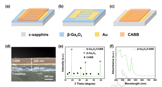
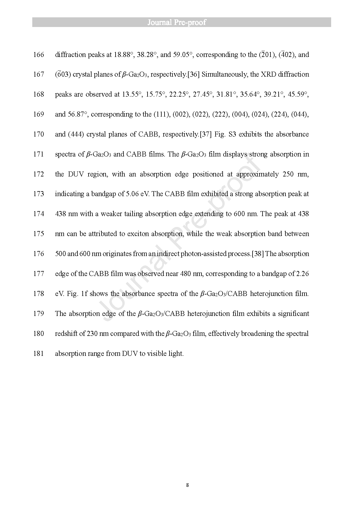
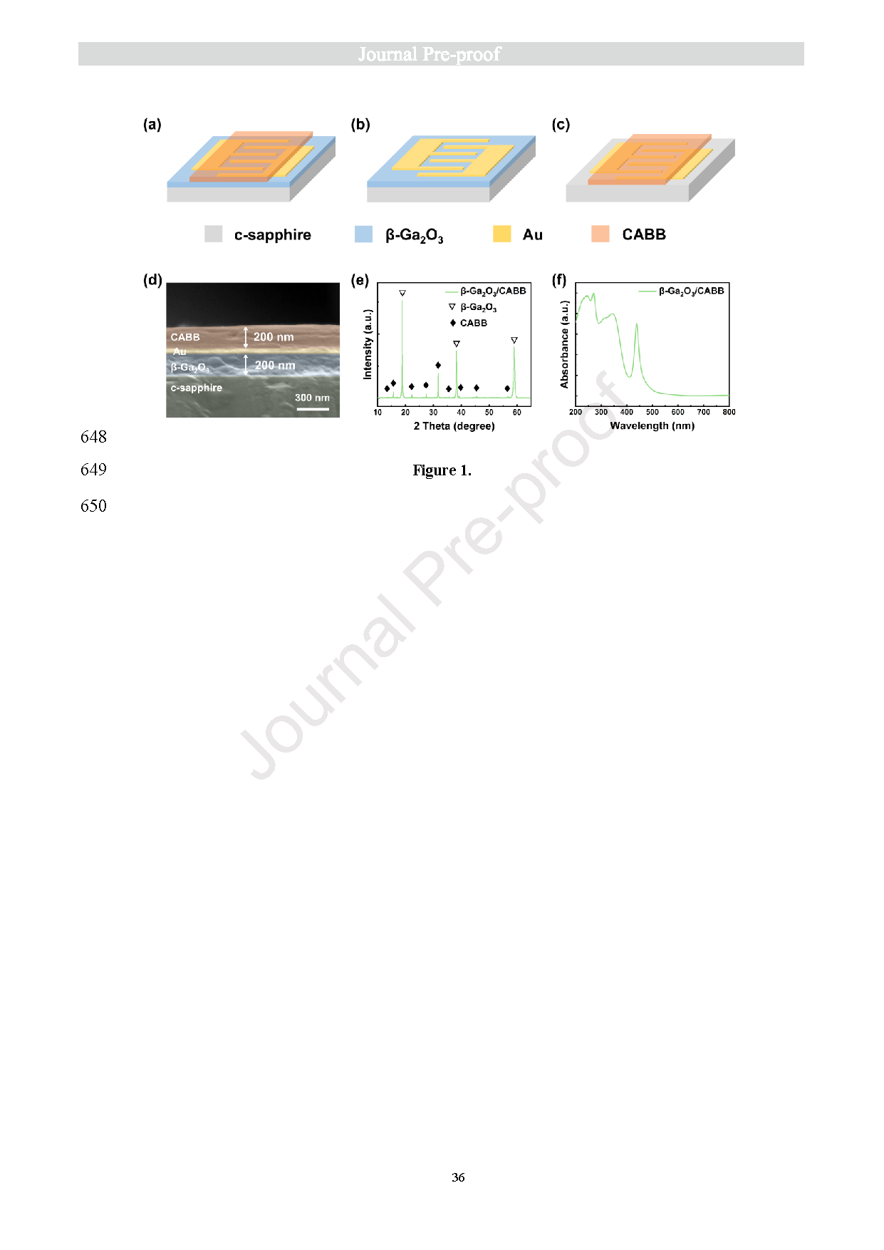
Fig. 1. Planar schematic illustration of the (a) β-Ga2O3/Au/CABB PD, (b) MSM β-Ga2O3 PD, (c) MSM CABB PD. (d) The cross-section SEM image of the β-Ga2O3/Au/CABB PD. (e) XRD patterns of the β-Ga2O3/CABB heterojunction film. (f) Absorbance spectra of the β-Ga2O3/CABB heterojunction film.
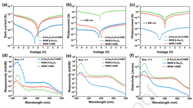
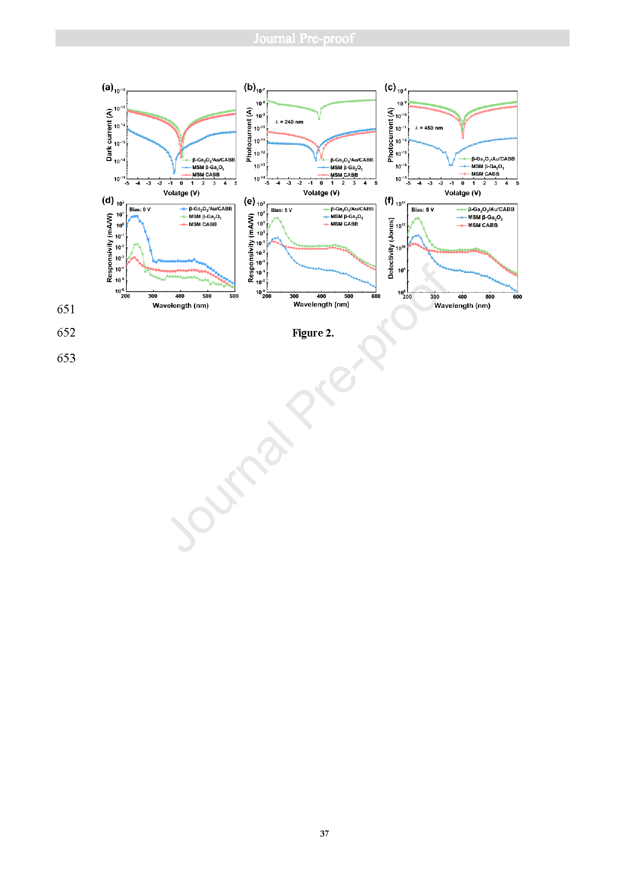
Fig. 2. The photoelectric performance of β-Ga2O3/Au/CABB PD, MSM β-Ga2O3 PD, and MSM CABB PD is presented as follows: (a) a comparative analysis of the I‒V curves in dark conditions; (b) I‒V curves under 240 nm illumination; (c) I‒V curves under 450 nm illumination; (d) responsivity curve at 0 V bias; (e) responsivity curve at 5 V bias; (f) detectivity curve at 5 V bias.
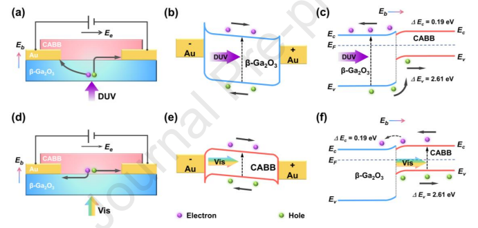
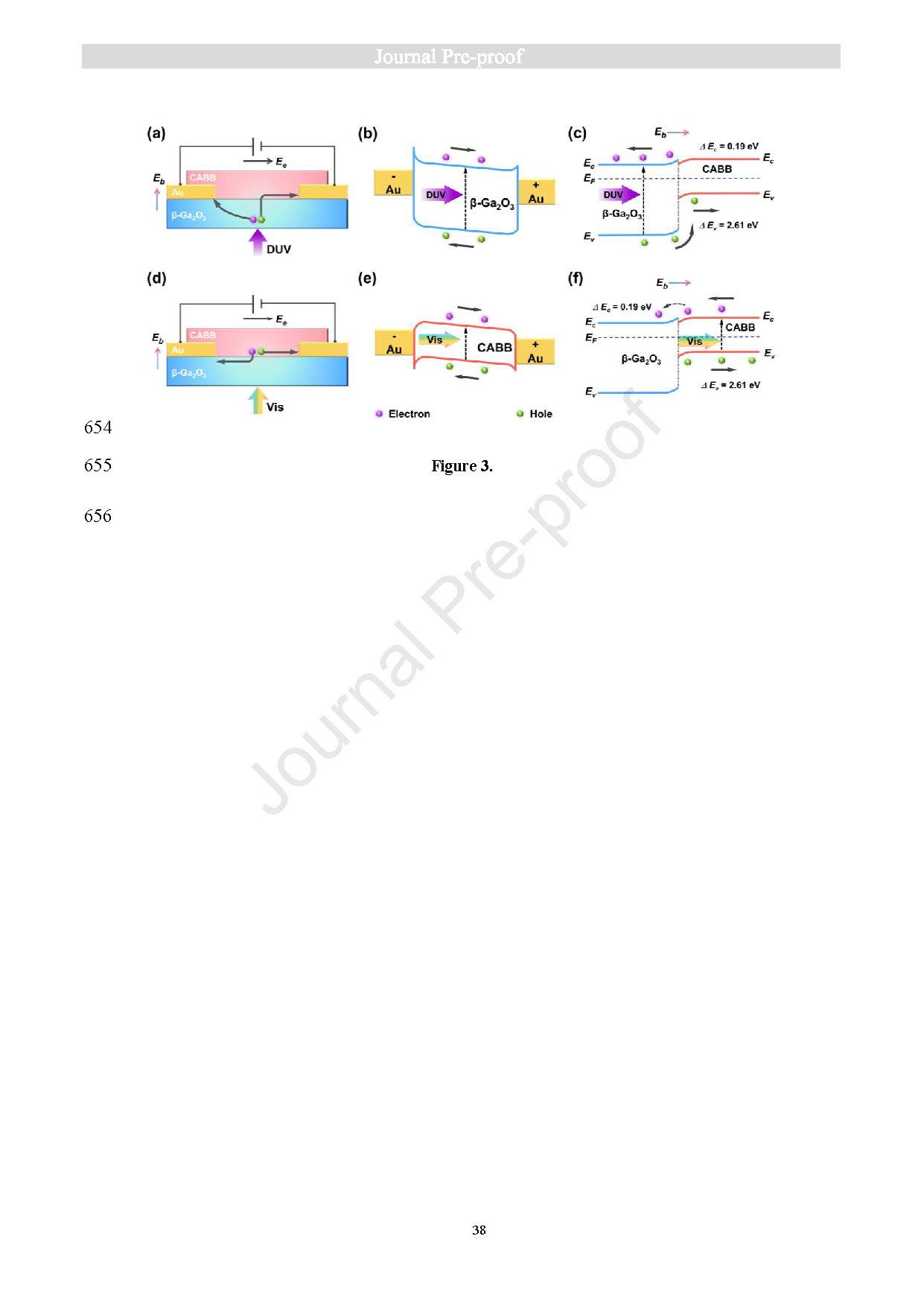
Figure 3. (a) Schematic diagram of carrier transport process in the β-Ga2O3/Au/CABB PD under DUV illumination. The energy band diagram under DUV illumination of (b) the β-Ga2O3/Au Schottky junction and (c) the β-Ga2O3/CABB heterojunction. (d) Schematic diagram of carrier transport process in the β-Ga2O3/Au/CABB PD under visible illumination. The energy band diagram under visible light illumination of (e) the Au/CABB ohmic contact and (f) the β-Ga2O3/CABB heterojunction.
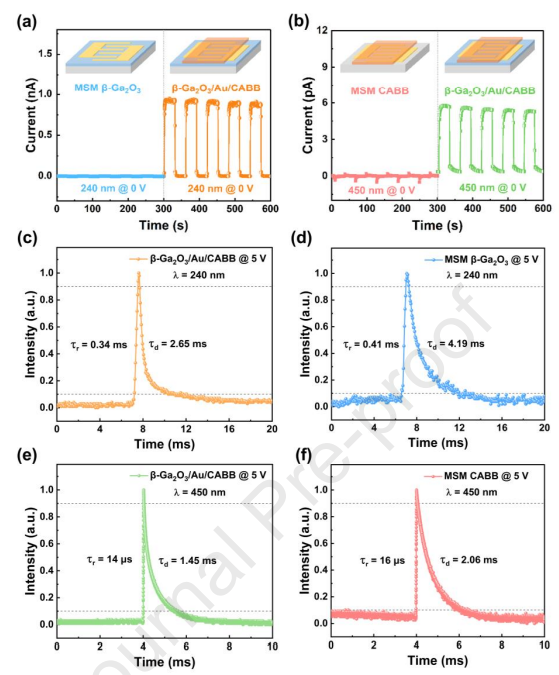
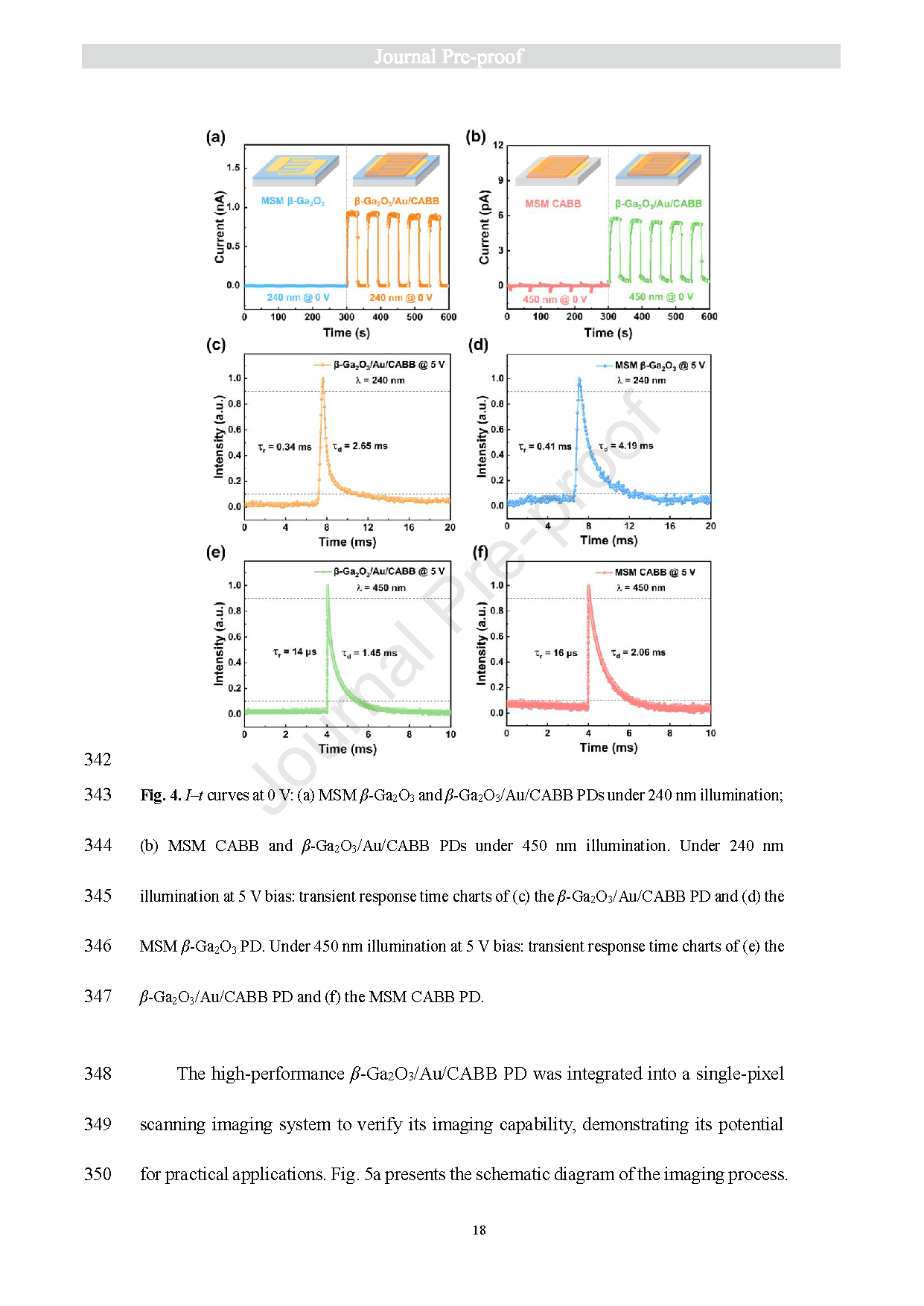
Fig. 4. I‒t curves at 0 V: (a) MSM β-Ga2O3 and β-Ga2O3/Au/CABB PDs under 240 nm illumination; (b) MSM CABB and β-Ga2O3/Au/CABB PDs under 450 nm illumination. Under 240 nm illumination at 5 V bias: transient response time charts of (c) the β-Ga2O3/Au/CABB PD and (d) the MSM β-Ga2O3 PD. Under 450 nm illumination at 5 V bias: transient response time charts of (e) the β-Ga2O3/Au/CABB PD and (f) the MSM CABB PD.
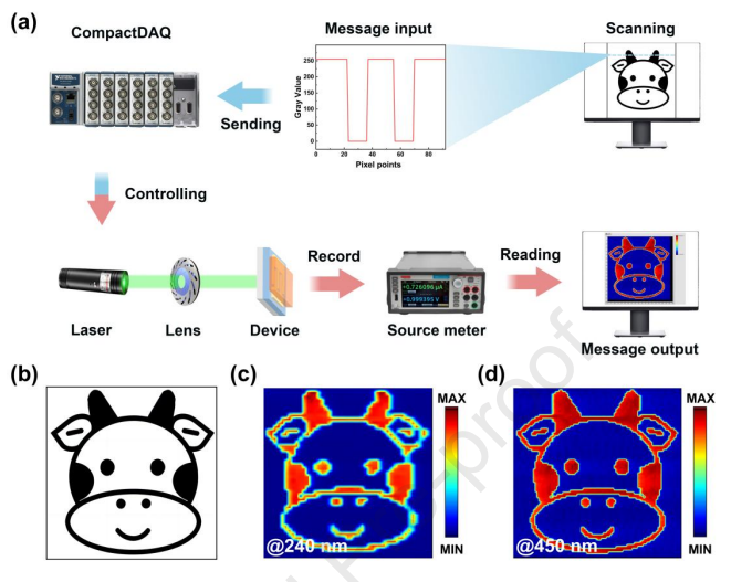
Fig. 5. The imaging capability of the β-Ga2O3/Au/CABB PD. (a) Schematic diagram of the single pixel scanning imaging system. (b) Target pattern intended for imaging. (c) Imaging results obtained under 240 nm illumination. (d) Imaging result obtained under 450 nm illumination.
DOI:
doi.org/10.1016/j.mtphys.2025.101935