Paper Sharing
【Domestic Papers】Electronic Excitation-Driven β-Ga₂O₃ Metastability Transformation and Self-Organization Mechanism: β→κ/γ/δ Phases
日期:2025-12-11阅读:501
Researchers from the Shandong University have published a dissertation titled "Electronic Excitation-Driven β-Ga2O3 Metastability Transformation and Self-Organization Mechanism: β→κ/γ/δ Phases" in Advanced Materials.
Background
β-Ga₂O₃ is one of the most promising ultrawide-bandgap semiconductors for power electronics, yet the metastable phase transitions among its polytypes (κ, γ, δ, etc.) remain poorly understood. Previous studies have largely relied on thermally driven or ion-beam–induced structural modulation, but these approaches typically introduce high defect densities, uncontrollable phase-transition pathways, and considerable material damage. This work focuses on an emerging mode of material regulation—electron-excitation–driven metastability transformation and self-organization in β-Ga₂O₃. However, prior experiments lacked direct evidence capable of capturing the formation mechanisms of different phases, stress-induced lattice distortion, and defect-evolution pathways, and they did not provide a unified interpretation of the energetic relationships and kinetic evolution among these phases.
In this study, we systematically explore a strategy that tailors the optoelectronic response of β-Ga₂O₃ by irradiation-induced structural transitions and strong electron-excitation–mediated defect engineering. Irradiation triggers a multiphase self-organization process (β → κ → γ → δ), where defect-mediated transitions dynamically modulate the strain-field distribution and interfacial electronic structure. This enables programmable control of nonlinear optoelectronic behavior and reveals the intrinsic correlations and underlying mechanisms among multiphase structures, dominant defect states, and specific photoelectric properties. These findings establish a foundation for targeted design and development of fourth-generation semiconductors. By identifying key conditions for optimized defect engineering, this work provides substantive implications for the processing, fabrication, and practical application of electronic materials.
Abstract
Irradiation-driven multiphase self-organization presents emergent opportunities for the customization of nanoscale engineering properties, dynamically tuning strain-field distributions and interfacial electronic structures. Responding to intense electronic excitation-induced energy deposition, the dominant phase transformations, with varying Gibbs free energy △Gof, are confirmed as β → κ → γ → δ that are located in specific microregions for Gallium (III) oxide (Ga2O3), as follows: (i) Surface-localized interstitial accumulation under compressive stress triggers β → δ via semi-coherent interface formation. (ii) Tensile stress within latent tracks drives vacancy-mediated oxygen layer truncation (4/12 periodicity along ⟨0001⟩), stabilizing coherent 4H (ABCB) κ and 3C (ABC) β (ABC) interfaces through strain-compensated octahedral distortion. (iii) Screw dislocation-mediated lattice relaxation induces β → γ via cation disordering (Ga3⁺ occupancy at β-interstitial sites), forming metastable spinel γ with mixed occupancy across 16d/8a Wyckoff sites. Irradiation-driven β-Ga2O3→κ/γ/δ transitions, as mechanistically revealed via inelastic thermal spike (i-TS) calculations and molecular dynamics simulations, induce defect-mediated nonlinear photoresponse, critical for optoelectronic engineering.
Conclusion
The underlying mechanisms of temperature-driven phase trans formations and diffusion-driven defect microstructures in β-Ga2O3 and Sn-doped β-Ga2O3 under intense electronic excitation: β → κ and β → δ phase transformations, each emerging in the surface and latent track damage regions, were found to be accompanied by a range of defects predominantly characterized by VO and Gai. During the reconstructive transformation of oxygen sublattice from 3C cubic (ABC) to 4H (ABCB) hexagonal and hematite-like (ABC) structure, interstitial atoms (Gai and Oi) are transported to the near-surface, creating positive pressure. Vacancy-type defects (VGa and VO), associated with negative pressure, form within the irradiated microregion. This process is accompanied by energy absorption that is inversely proportional to the volume of transformed material. A strain engineering methodology is developed to determine the lattice parameters both parallel and normal to the sample surface in individual layers of β-Ga2O3 single-crystalline lattices. This approach is based on the analysis of high-angle X-ray diffraction measurements combined with reciprocal space mapping. Anisotropic lat tice expansion induced by strain relaxation and various defect component distributions is quantitatively evaluated. Accompanied by an increase in Δ Gof attributed to the formation of a semi coherent structure, the interplay between positive and negative pressure driven by the spatial defect distribution governs local ized phase transitions in microregions from β → κ → δ phases, with reversed stability order of β>κ>δ. These specific phase transition paths combined with defect engineering produced advantageous effects critical to the device operation of transistors and photodetectors within a specific threshold, achieving ultrahigh photoconductive gain by increasing carrier mobility and effective carrier concentration.
Project Support
This research was funded by the National Natural Science Foundation of China (No.12322514,12405313), the Shandong Natural Science Foundation (No. ZR2024QA055), and the National Laboratory of Heavy Ion Accelerator in Lanzhou. EZ was supported by the Center for Nanophase Materials Sciences (CNMS), which is a US Department of Energy, Office of Science User Facility at Oak Ridge National Laboratory.
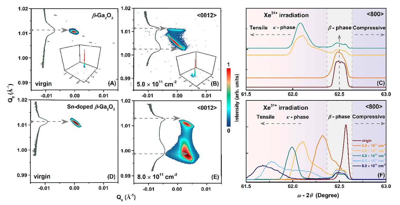
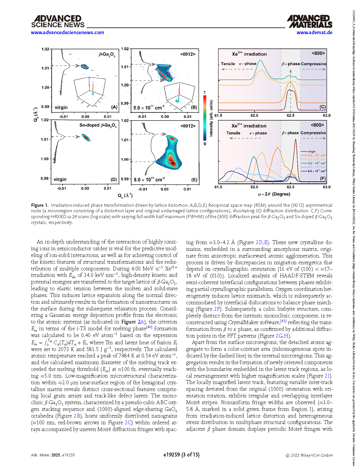
Figure 1. Irradiation-induced phase transformation driven by lattice distortion. A, B, D, E) Reciprocal space maps (RSMs) around the ⟨0012⟩ asymmetrical node (a micro-region consisting of a distortion layer and original undamaged lattice configurations), illustrating the 3D diffraction distribution. C, F) Corresponding HRXRD ω–2θ scans (log scale) with varying full-width at half-maximum (FWHM) of the ⟨800⟩ diffraction peak for β-Ga₂O₃ and Sn-doped β-Ga₂O₃ crystals, respectively.

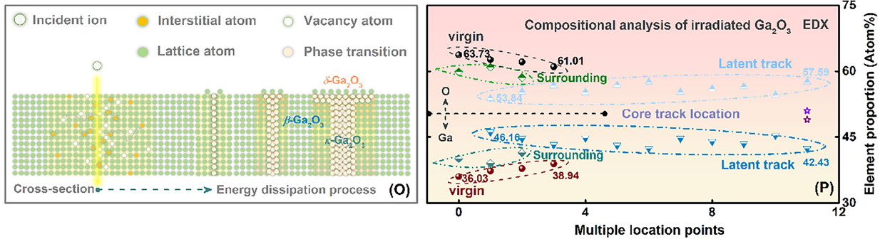
Figure 2. Irradiation-induced uneven distribution of specific phase transformations driven by thermal spike response. A) The energy deposition to the electronic and atomic subsystems under 4.00 MeV u−1 Xe³¹⁺ irradiation in β-Ga₂O₃ (Eele = 34.0 keV nm⁻¹, fluence: 5.0 × 10¹¹ cm⁻²). B) Low-magnification cross-sectional micrographs within ≈2 μm depth range. C–H) Higher-magnification images representing the orientation relationships for β → δ transformation, together with the acquired FFT patterns and corresponding diffraction simulations. I–N) Higher-magnification images representing the orientation relationships for β → κ transformation, together with the acquired FFT patterns and corresponding diffraction simulations. FFT patterns of the β phase, δ phase, and κ phase from the marked HRTEM areas confirm the orientation and structural relationships, i.e.: {200}β // {-211}δ,{200}β // {20-4}κ. O) Schematic representation summarizing the evolution features.P) Right: Energy-dispersive X-ray spectroscopy (EDS) spectrum exhibiting the elemental distribution in the latent track and surrounding microregions; detailed maps for local atomic percentage are shown in the frame underneath.

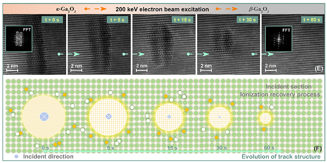
Figure 3. Stress-driven enhanced Gibbs free energy and specific phase transformation recovery behavior. A,B) Normalized oxygen K-edge recorded via DD-EELS of the latent track and surrounding regions, along with the corresponding atomic configurations of defects. C) Left: Evolution of ΔGof from β-Ga₂O₃ → κ-Ga₂O₃ → δ-Ga₂O₃. D,E,F) In situ investigation of recovery dynamics in response to electron-beam-bombardment-induced recrystallization at 200 keV accelerating voltage (5, 15, 30, 60 s intervals).

Figure 4. Irradiation-induced multiphase formation from MD simulations. A,B,E,F) Different phase-transformation structures observed from MD simulations of irradiation-induced heating along the X and Y planes. A series of Ga and O sublattices initially transform into a disordered, amorphous molten phase at 0 ps and 100 ps, followed by a gradual phase transformation. C,D) RDFs for the β and γ configurations of Ga₂O₃, with cutoff distances defined based on the shortest side length of the corresponding unit cells. G–J) Dynamic recrystallization and formation of phase-transformation structures centered on a thermal spike with energy deposition under −15 GPa pressure. K,L) Transformation of the β → κ phase within 1000 ps. M) RDFs for the κ-Ga₂O₃ polymorph. N,O,Q) The β → γ → δ structure transformation at a pressure of 15 GPa. P) Orientation relationship between the two phases: oxygen layers reconstructed from 3C (ABC) ccp (right) to 4H (ABCB) hcp (left).
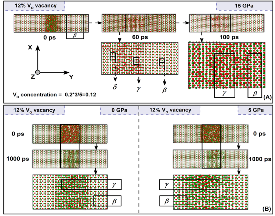
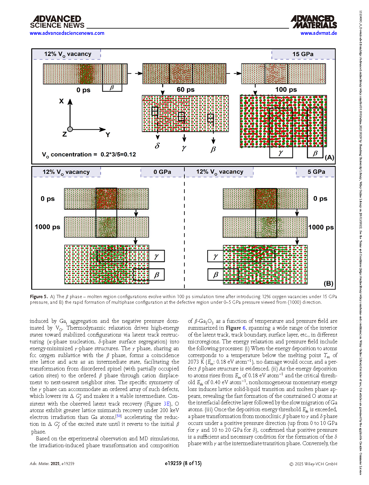
Figure 5. A) The β-phase/molten-region configurations evolving within 100 ps simulation time after introducing 12% oxygen vacancies under 15 GPa pressure. B) Rapid formation of a multiphase configuration in the defective region under 0–5 GPa pressure, viewed from the ⟨1000⟩ direction.
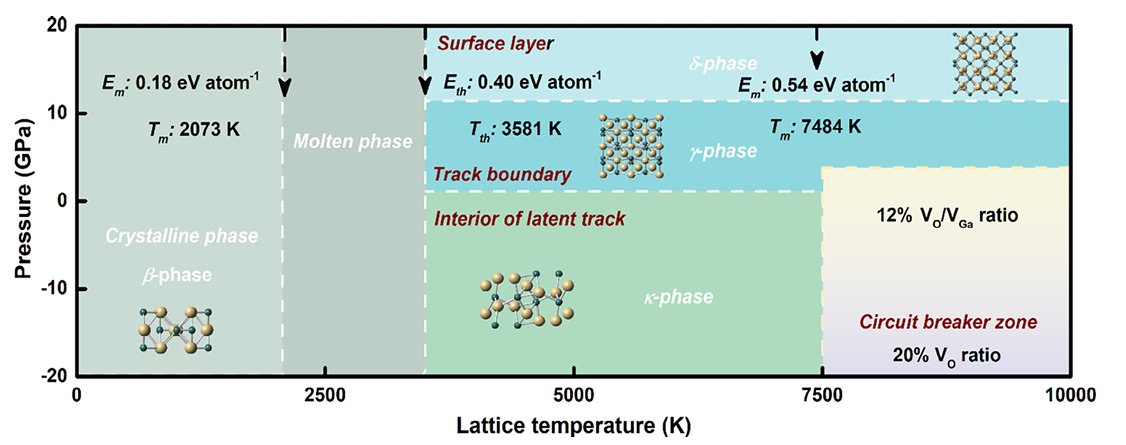
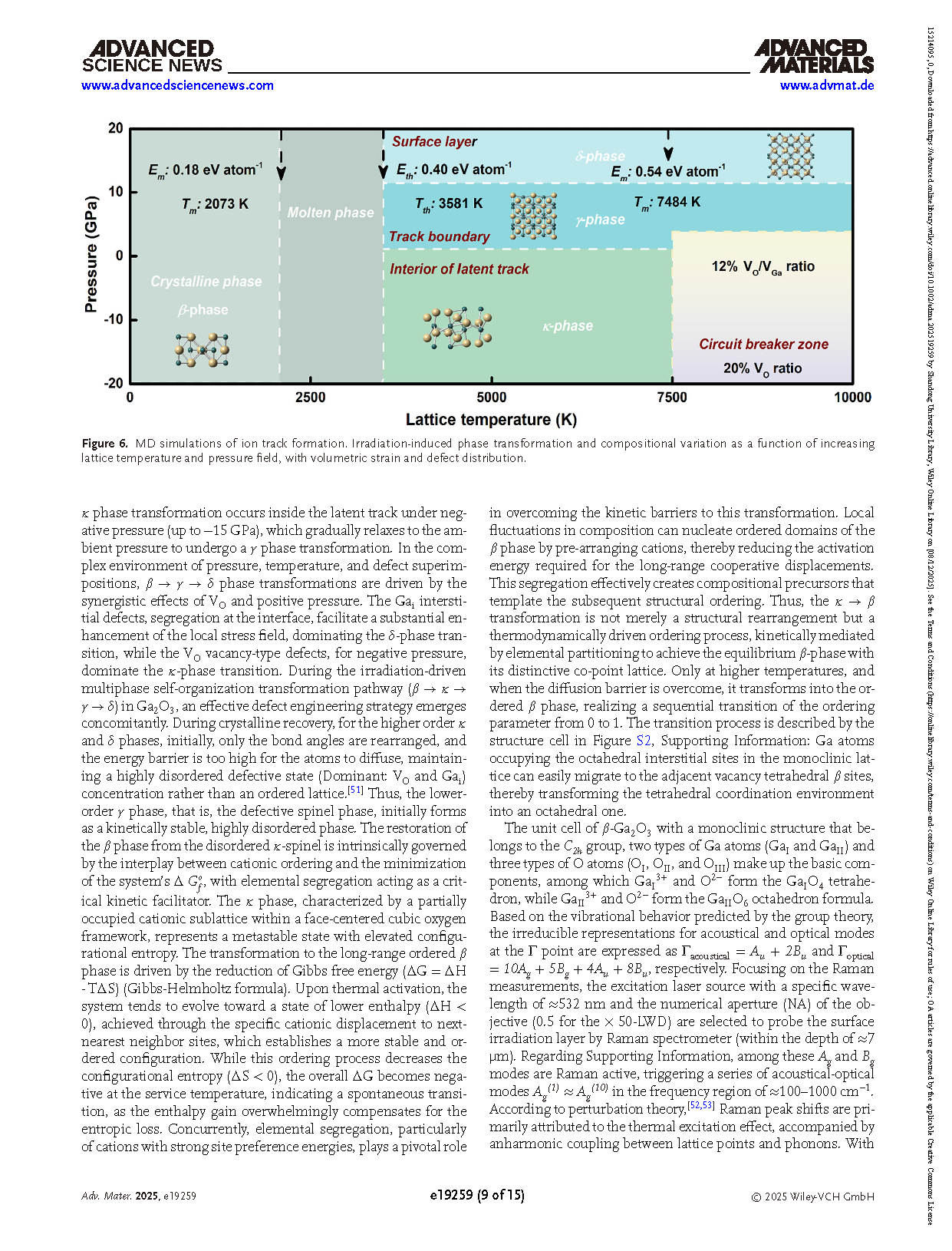
Figure 6. MD simulations of ion track formation. Irradiation-induced phase transformation and compositional variation as a function of increasing lattice temperature and pressure field, with volumetric strain and defect distribution.
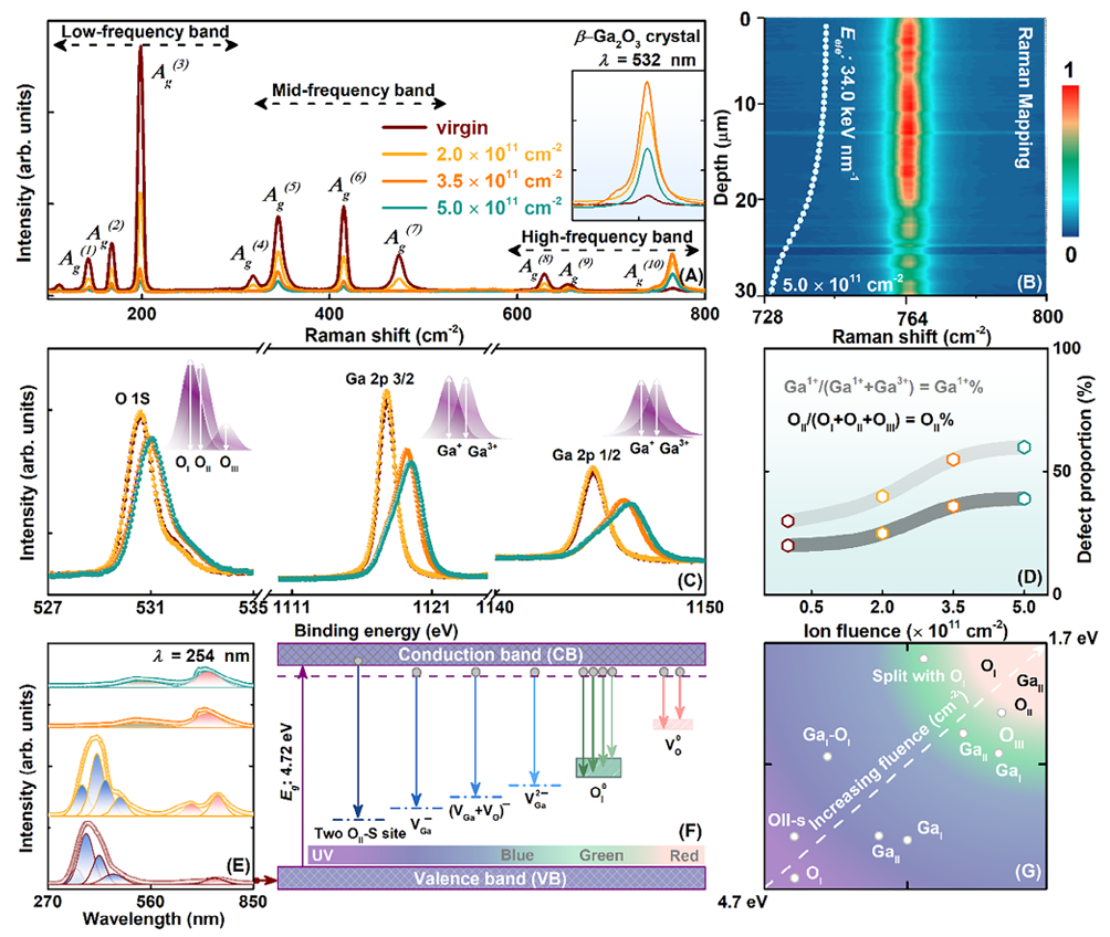
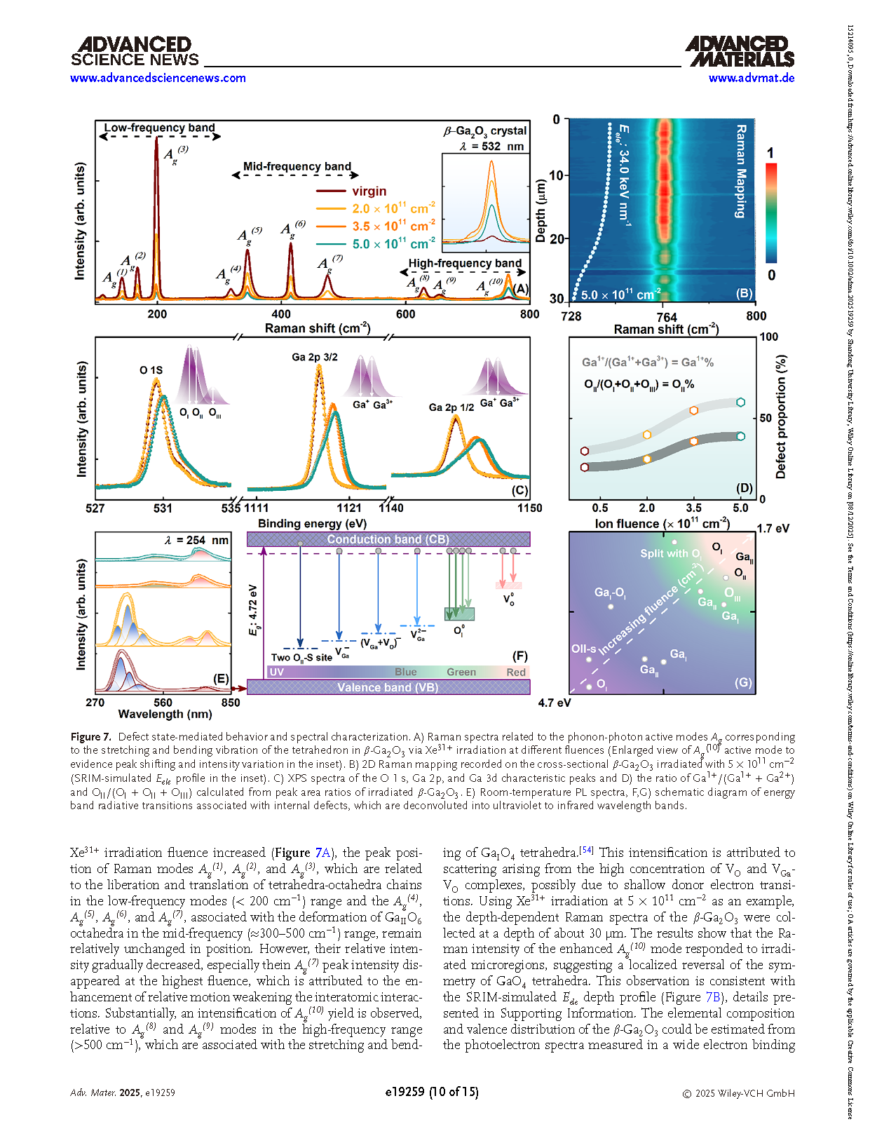
Figure 7. Defect state-mediated behavior and spectral characterization. A) Raman spectra related to the phonon–photon active modes Ag corresponding to the stretching and bending vibration of the tetrahedron in β-Ga₂O₃ via Xe³¹⁺ irradiation at different fluences (enlarged view of the Ag(10) active mode showing peak shifting and intensity variation in the inset). B) 2D Raman mapping recorded on the cross-sectional β-Ga₂O₃ irradiated with 5 × 10¹¹ cm⁻² (SRIM-simulated Eₑₗₑ profile in the inset). C) XPS spectra of the O 1s, Ga 2p, and Ga 3d characteristic peaks. D) Ratio of Ga¹⁺/(Ga¹⁺ + Ga²⁺) and OII/(OI + OII + OIII) calculated from peak area ratios of irradiated β-Ga₂O₃. E) Room-temperature PL spectra. F,G) Schematic diagram of energy-band radiative transitions associated with internal defects, deconvoluted into ultraviolet to infrared wavelength bands.
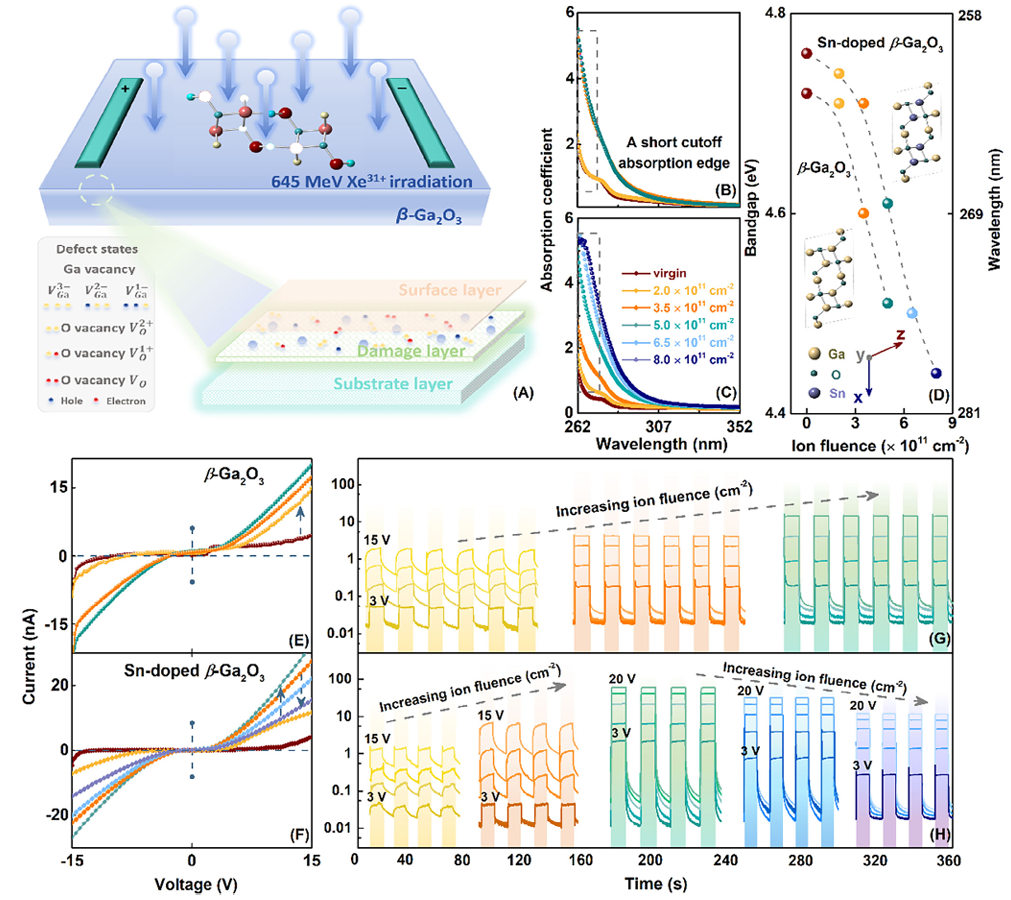
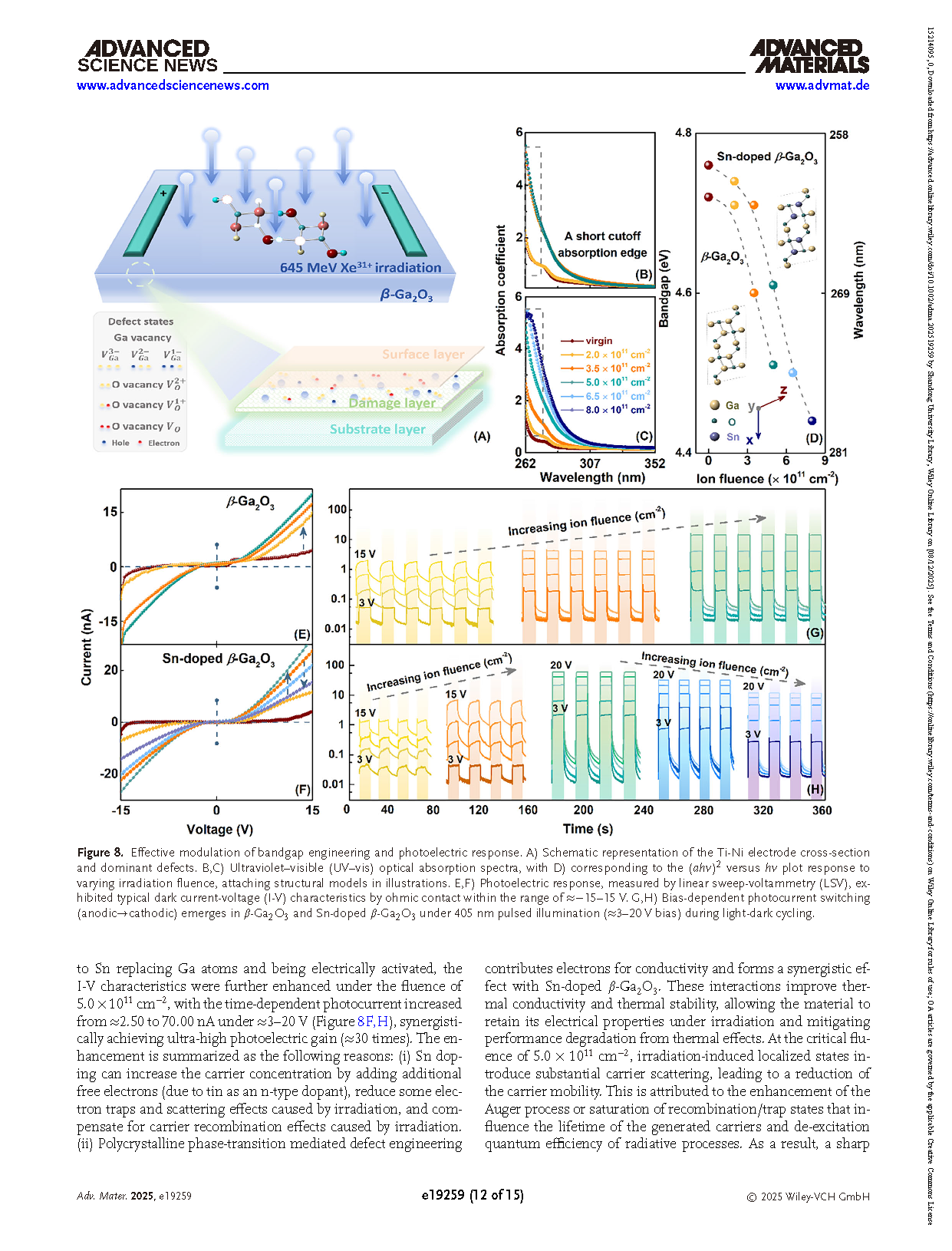
Figure 8. Effective modulation of bandgap engineering and photoelectric response. A) Schematic representation of the Ti–Ni electrode cross-section and dominant defects. B,C) Ultraviolet–visible (UV–vis) optical absorption spectra. D) Corresponding (αhv)² versus hv plot in response to varying irradiation fluence, with structural models shown in the illustrations. E,F) Photoelectric response measured by linear sweep voltammetry (LSV), exhibiting typical dark current–voltage (I–V) characteristics with ohmic contact behavior in the range of ≈ −15–15 V. G,H) Bias-dependent photocurrent switching (anodic → cathodic) emerging in β-Ga₂O₃ and Sn-doped β-Ga₂O₃ under 405 nm pulsed illumination (≈3–20 V bias) during light–dark cycling.
DOI:
doi.org/10.1002/adma.202519259