Paper Sharing
【International Papers】Structural insights into nucleation and grain orientation in β-Ga₂O₃ films grown by MOVPE on off-axis 4H-SiC substrates
日期:2025-12-11阅读:440
Researchers from the Institute for Microelectronics and Microsystems, IMM-CNR have published a dissertation titled "Structural insights into nucleation and grain orientation in β-Ga2O3 films grown by MOVPE on off-axis 4H-SiC substrates" in Applied Surface Science.
Background
Gallium oxide (Ga2O3) is an ultrawide-bandgap semiconductor that has attracted much attention as suitable material for the fabrication of power electronic devices and UV-C photodetectors. This material is very prone to polymorphism and there are five known phases, namely α (hexagonal), β (monoclinic), γ (cubic spinel), δ (cubic), κ (orthorhombic). The β-Ga2O3 polymorph is so far the most investigated because of its peculiar properties: thermodynamic stability, bandgap of about 4.9 eV, estimated breakdown field larger than 6 MV/cm and Baliga figure of merit > 3000. Furthermore, β-phase single crystals can be grown from the melt, which makes the production of good-quality substrates and homoepitaxy possible. These characteristics make this material an ideal candidate for high-power electronic devices, such as vertical Schottky diodes and FETs. However, its low-symmetry monoclinic structure and its anisotropic low thermal conductivity still trigger significant technical issues, such as undesired cleavage and poor heat dissipation.
Abstract
In this work, β-Ga2O3 was deposited by low-pressure metal organic vapour phase epitaxy on 4° off-axis 4H-SiC. This substrate has a high thermal conductivity and can enable a more effective heat dissipation in vertical power devices compared to the low-conductivity β-Ga2O3 homo-substrates. The obtained heteroepitaxial films were characterized by X-ray diffraction and transmission electron microscopy. Results show that β-Ga2O3 films are composed of grains with three specific in-plane orientations, all characterized by planes of oxygen atoms arranged in a pseudo hexagonal geometry, namely the (-201), which is the main orientation, the (101), which remains confined near the interface, and the two equivalent (310) and (3-10), which instead tend to expand laterally and grow up to the film surface. The interface between β-Ga2O3 and 4H-SiC was thoroughly investigated by electron diffraction and high-resolution scanning transmission electron microscopy. The outcome of this work provides a deeper understanding of the nucleation and growth of β-Ga2O3 on 4° off-axis 4H-SiC substrates, focusing on the competition between step-flow and island growth mechanisms.
Highlights
● β-Ga2O3 films were grown by MOVPE on 4° off-axis 4H-SiC substrates.
● TEM and XRD analyses revealed three distinct grain orientations: (-201), (101), and (310).
● The (-201) orientation dominates, while (101) grains remain confined near the interface.
● (310) grains nucleate sparsely but expand laterally up to the film surface.
● Step-flow growth is disrupted, favoring 2D nucleation and 3D island formation.
Conclusions
Films of β-Ga2O3 were deposited by MOVPE on 4° off-axis 4H-SiC substrates and characterized by XRD and TEM to investigate their nucleation and growth mechanisms. TEM analyses enabled the formulation of a sound hypothesis regarding the initial stage of β-Ga2O3 films growth on SiC substrates. In the monoclinic structure of β-Ga2O3, four different pseudo-hexagonal oxygen planes can be identified: (-201), (101) , (310) and (3-10), the last two being equivalent. Despite the similarity in the oxygen sublattices, these orientations differ in the arrangement of gallium atoms. Experimental evidence indicates that these pseudo-hexagonal oxygen planes govern the nucleation of β-Ga2O3 films at the interface with the substrate. Indeed, grains oriented with the (-201), (101), (310) and (3-10) planes parallel to the (0001) 4H-SiC basal plane were observed, with the (-201) orientation being statistically the prevalent one. It was found that (-201)-oriented grains nucleate always with a first plane of octahedral Ga atoms above the SiC terraces; (101) -oriented grains are confined near the interface, extending only a few tens of nanometers, before being fully overgrown; (310) -oriented grains nucleate less frequently than (-201) grains but can expand laterally and reach the surface. The presence at the interface of small hemispherical domains, voids at the step edges and grains with different orientations suggest that step-flow growth does not occur, despite the stepped nature of the substrate surface. Instead, a 2D followed by a 3D island growth on the terraces is observed.
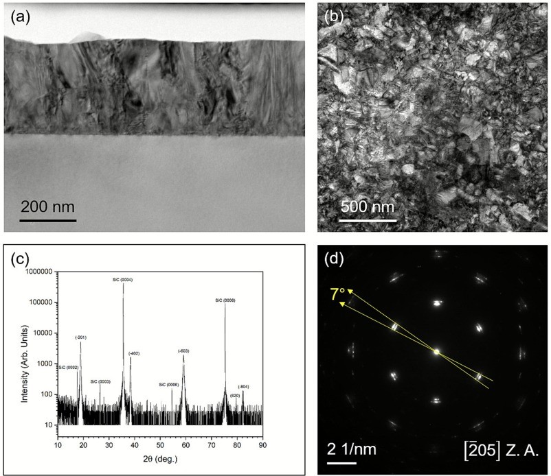
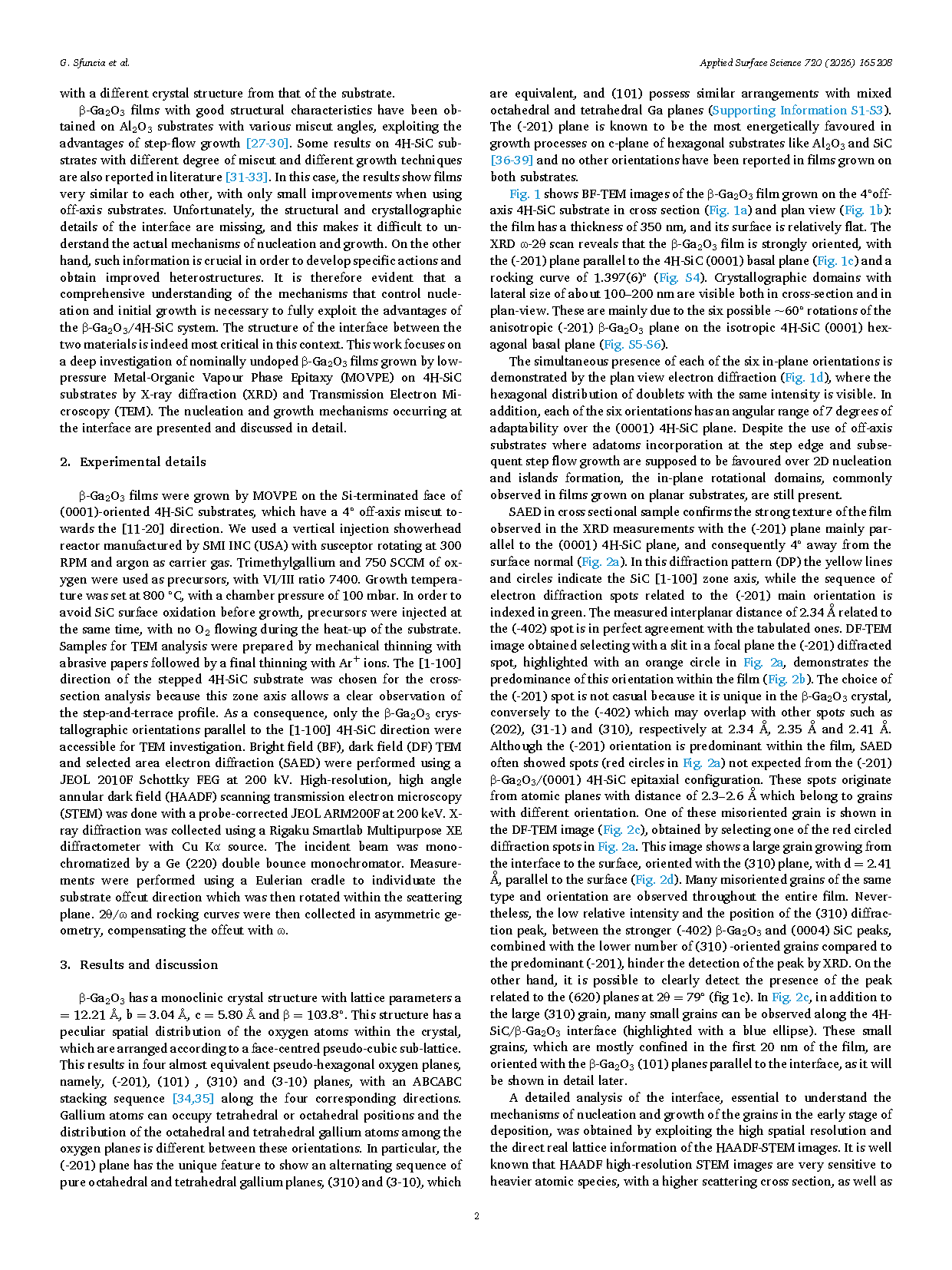
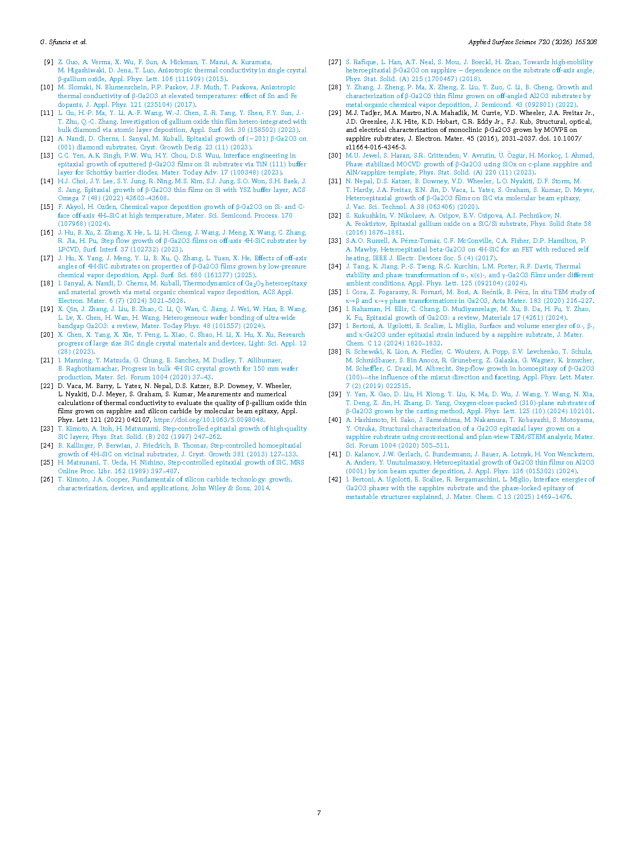
Fig. 1. (a) Cross section and (b) plan view TEM images of β-Ga2O3 grown on 4°off-axis 4H-SiC substrate. (c) XRD ω-2θ diffractogram. (d) in-plane electron diffraction along [-205] zone axis.
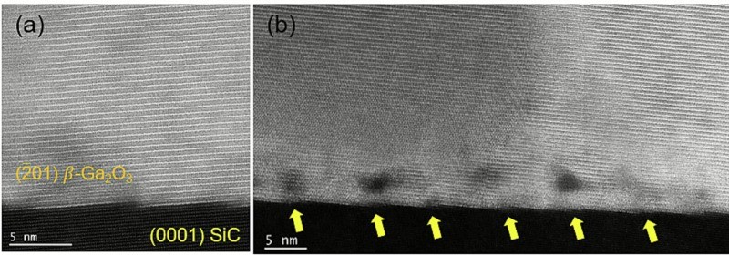
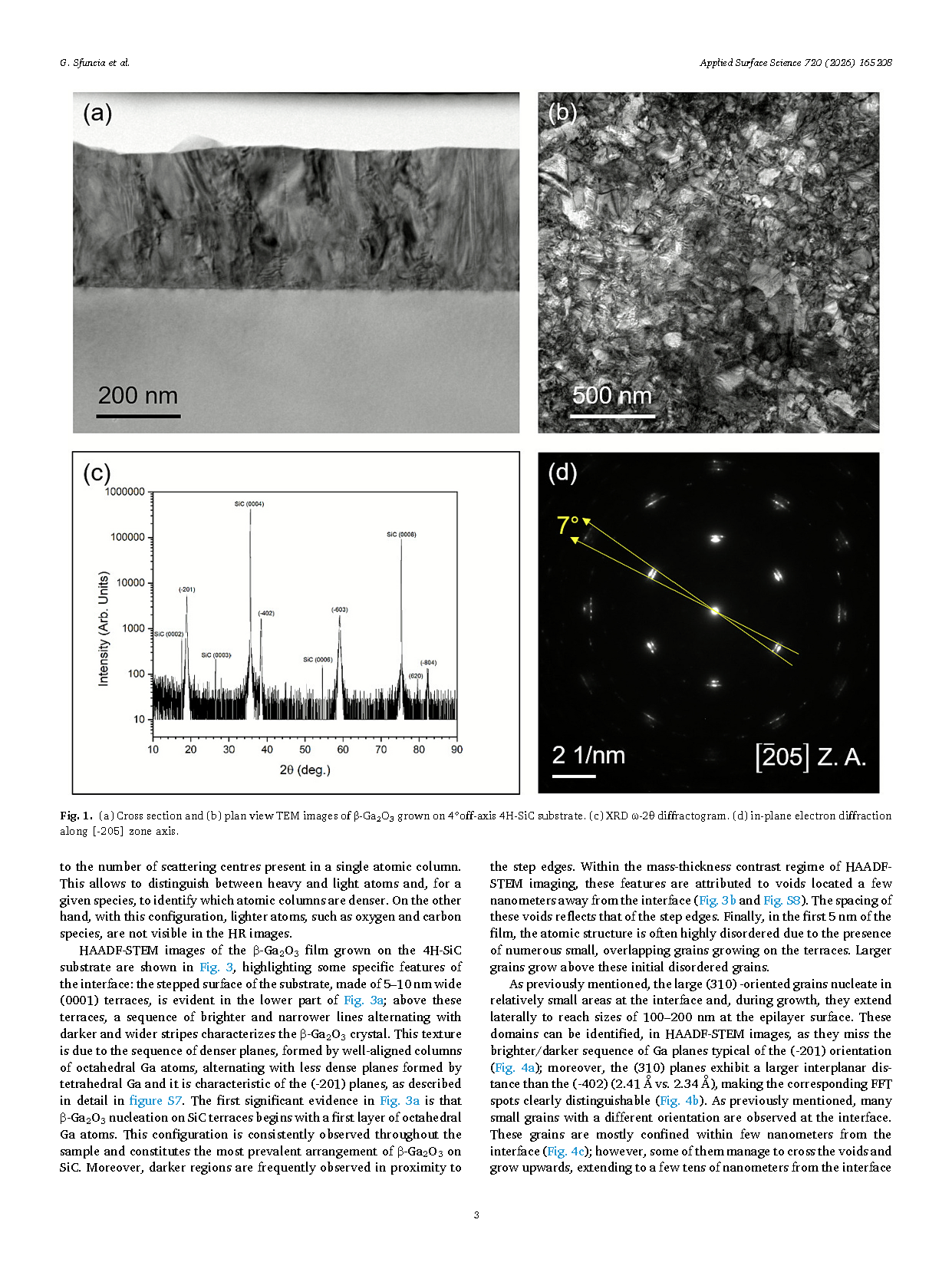
Fig. 2. (a) SAED acquired in the circled area in (b). (b) DF-TEM image obtained selecting the β-Ga2O3 (-201) diffraction spot, highlighted by an orange circle in (a). (c) DF-TEM image obtained selecting one of the red circles in (a). (d) DP acquired in the purple circled region in (c).
Fig. 3. High resolution HAADF STEM images of the β-Ga2O3/4H-SiC interface. (a) (0001) SiC terraces with (-201) octahedral Ga planes grown on it. (b) Voids at 5 nm from the interface, in correspondence with the step edges (yellow arrows).
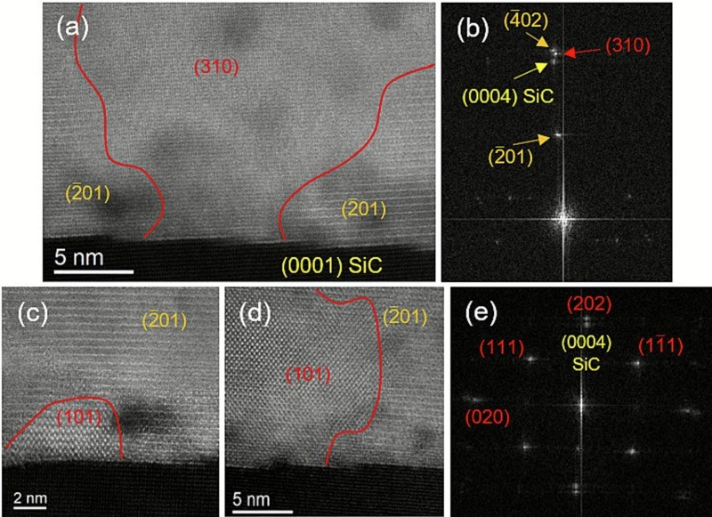
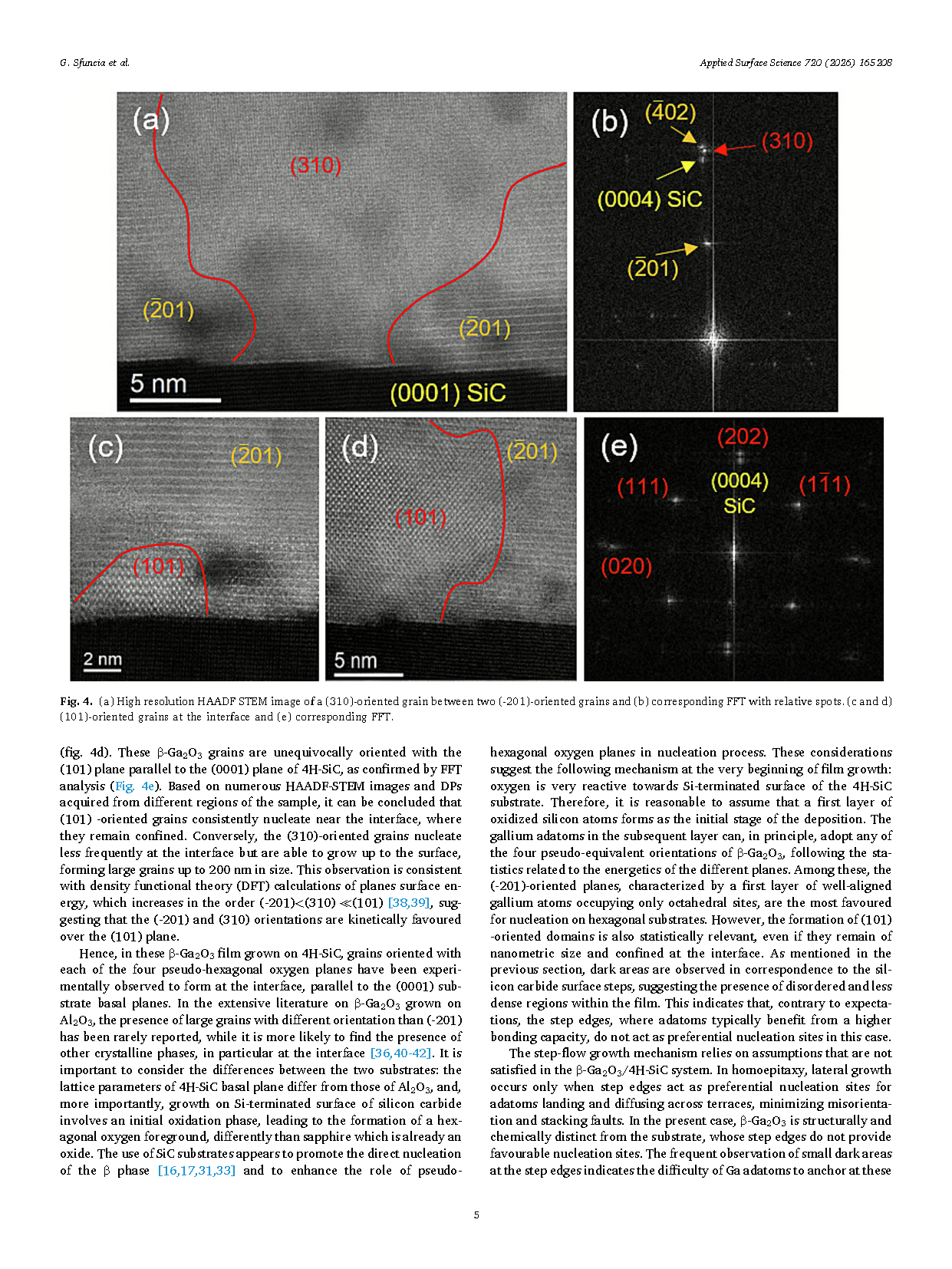
Fig. 4. (a) High resolution HAADF STEM image of a (310)-oriented grain between two (-201)-oriented grains and (b) corresponding FFT with relative spots. (c and d) (101)-oriented grains at the interface and (e) corresponding FFT.
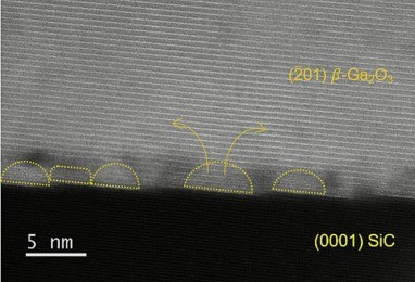
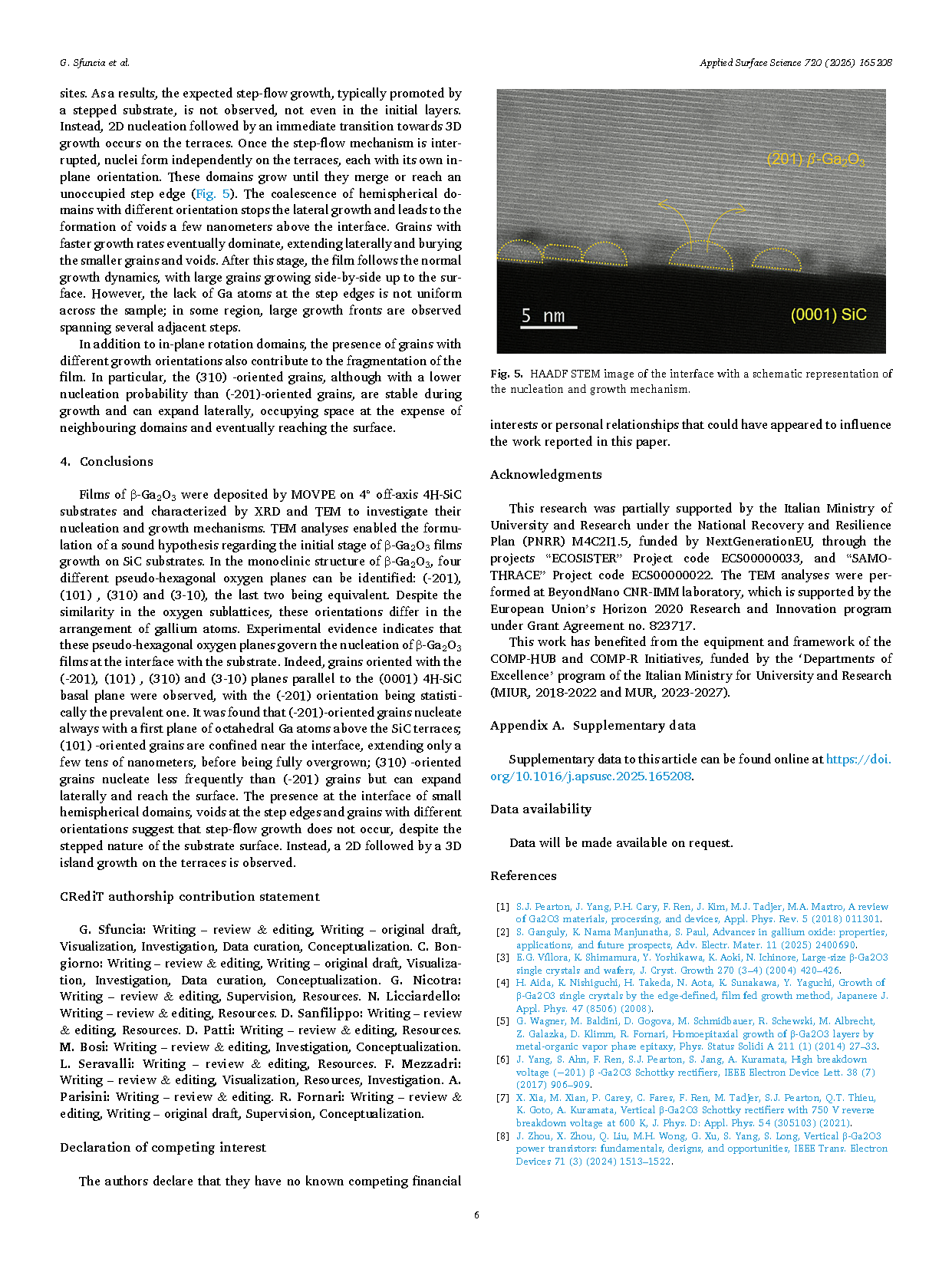
Fig. 5. HAADF STEM image of the interface with a schematic representation of the nucleation and growth mechanism.
DOI:
doi.org/10.1016/j.apsusc.2025.165208