


Member News
【Member News】Top 30 Candidates for thnnual Advances in China’s Third-Generation Semiconductor Technology: Major Breakthrough in 8-inch Gallium Oxide Single Crystals and Substrate Manufacturing by Garen Semiconductor
日期:2025-12-08阅读:580
To implement China’s innovation-driven development strategy, accelerate the cultivation of new quality productive forces, and highlight key technological advances in the nation’s third-generation semiconductor industry, the Program Committee of the 11th International Forum on Wide Bandgap Semiconductors & the 22nd China International Forum on Solid State Lighting (IFWS & SSLCHINA 2025) initiated the selection for the “Annual Top Ten Advances in China’s Third-Generation Semiconductor Technology.” In 2025, a total of 43 valid entries were collected and screened in compliance with the evaluation criteria. Based on expert voting by the Program Committee, 33 outstanding achievements have entered the final Top 30 candidates (in no particular order). These achievements will be introduced one by one—please stay tuned.
Major Breakthrough in 8-inch Gallium Oxide Single Crystals and Substrate Manufacturing
—Hangzhou Garen Semiconductor Co., Ltd.
Garen Semiconductor has achieved a major technological breakthrough, becoming the world’s first company to master the fabrication of 8-inch Gallium Oxide single crystals and substrates. Within just three years, the company completed a leap from 2 inches to 8 inches, setting a new record for rapid diameter scaling in the industry.
As a core material in ultrawide-bandgap semiconductors, Gallium Oxide features a bandgap of 4.85 eV and a high critical breakdown field of 8 MV/cm, serving as a foundational material for high-end power, RF, and optoelectronic devices. However, traditional growth methods rely heavily on precious metals, come with high costs, and are incompatible with mainstream silicon-based production lines. Leveraging its proprietary “casting method,” Garen Semiconductor has solved the twin-crystal defect challenge in single crystal growth and achieved breakthroughs in key technologies such as multiphysics-field coupling control and controlled doping. The company has developed a thermal-field system optimized for large-diameter crystal growth, enabling stable production with advantages of low cost, high efficiency, and excellent scalability. All technologies are covered by fully independent intellectual property rights.
This achievement fills the global technological gap in large-diameter Gallium Oxide crystals and substrates, helping China transition from “follower” to “leader” in the ultrawide-bandgap semiconductor domain and providing critical material support for fast charging in new energy vehicles, smart grids, and other high-end applications.
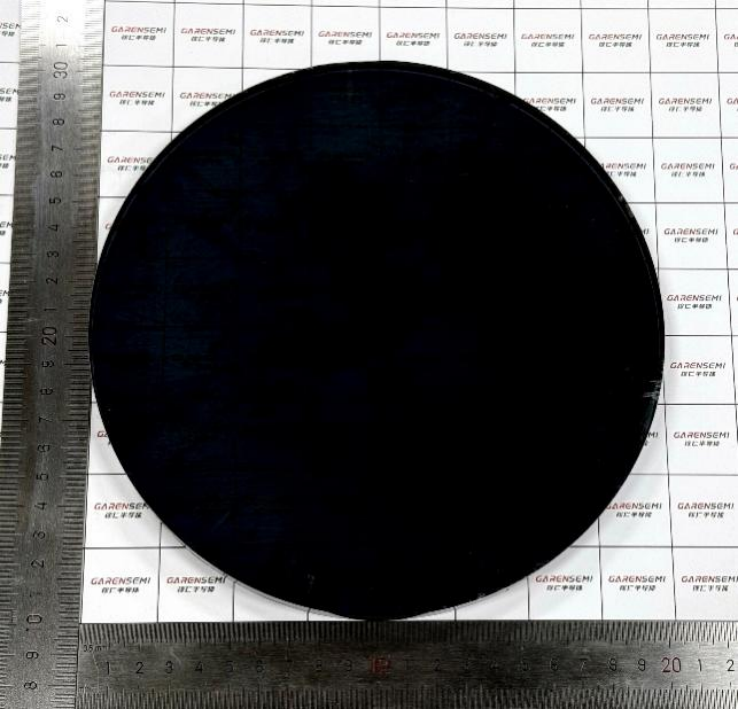
8-inch Gallium Oxide Single Crystal
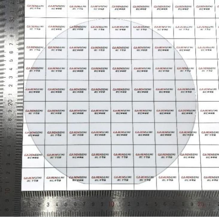
8-inch Gallium Oxide Substrate
Academic and Industrial Value
Academic Value
1.Product breakthrough:
The 8-inch Gallium Oxide single crystal and substrate represent the world’s first and are internationally leading.
2.Innovative crystal-growth method:
A proprietary, large-diameter Gallium Oxide crystal-growth method—the casting method—was developed.
This method does not require single-crystal seeds, involves fewer growth steps, enables a high degree of automation, and fills the domestic technological gap in casting-based Gallium Oxide crystal growth.
3.Precise thermal-field construction:
The company proposed a high-temperature thermal-field design using multilayer nested insulation, bottom-heating modules, and multi-coil configurations to adjust the temperature distribution within the crucible.
This enables real-time correction of temperature gradients, allowing precise control of crystal growth rates and preventing polycrystallization and cracks—thereby improving yield and quality for 8-inch Gallium Oxide crystals.
Industrial Value
1.Production-line compatibility:
The 8-inch Gallium Oxide product is compatible with existing 8-inch silicon device fabrication lines.
Compared with conventional EFG-type methods that rely on expensive precious metals, the casting method increases production efficiency by over 300% and reduces material costs by 60%, greatly lowering barriers for industrializing high-end power, RF, and optoelectronic devices.
2.Breaking international monopolies:
This breakthrough challenges the market dominance of companies such as NCT.
Garen Semiconductor currently holds the second-largest global market share, just behind NCT.
Its products provide critical domestic material support for fast charging in NEVs, high-efficiency power transmission, and high-voltage/high-frequency applications in national defense and aerospace—strengthening the security of China’s semiconductor supply chain.
Innovation Metrics
Comparative Analysis of β-Ga₂O₃ Crystals and Substrates (Domestic and International)
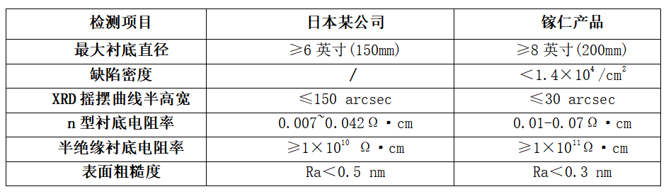
Garen Semiconductor vs. Company X (Japan): Company X has achieved mass production of 4-inch and R&D-level 6-inch substrates. Garen has achieved mass production of 6-inch and pilot production of 8-inch substrates.
Garen’s 8-inch Gallium Oxide substrates outperform those of Company X across all technical parameters, making them a viable replacement for imported products and establishing an internationally leading position.
Application Prospects
As a fourth-generation semiconductor material, Gallium Oxide offers an ultrawide bandgap and exceptionally high breakdown strength. Power devices based on Gallium Oxide exhibit higher voltage resistance, greater power capability, and lower losses, making them ideal for extreme environments such as high temperature, high voltage, and strong radiation.
Application fields include: National defense and aerospace, New energy vehicles, High-voltage power transmission, High-frequency, high-power systems.
In NEVs, Gallium Oxide materials can accelerate fast-charging technology and reduce charging times.
In smart grids, they improve transmission efficiency and reduce power losses.
In defense and aerospace, Gallium Oxide supports the development of high-voltage, high-temperature RF components, ensuring reliable operation in extreme conditions and enabling breakthroughs in critical applications.
Recommender’s Statement
This achievement, based on the fully proprietary “casting method,” overcomes core technological barriers in large-diameter Gallium Oxide production. It offers both academic and industrial significance and drives technological advancement in China’s semiconductor materials sector.
— Jiang Jiwei, Hangzhou Garen Semiconductor Co., Ltd.
Patent Portfolio
11 uthorized invention patents (9 domestic, 2 international),2 authorized utility model patents,18 invention patents under review.
