Paper Sharing
【Domestic Papers】An improved composite JTE technique with increased tolerance to interface charges for 2.8 kV β-Ga₂O₃ Schottky rectifier
日期:2025-12-08阅读:447
Researchers from the University of Science and Technology of China have published a dissertation titled "An improved composite JTE technique with increased tolerance to interface charges for 2.8 kV β-Ga2O3 Schottky rectifier" in Applied Physics Letters.
Project Support
This work was supported by the National Key Research and Development Program of China (Grant No. 2024YFE0205200), the National Natural Science Foundation of China under Grant Nos. U23A20358, 62474170, 62234007, and 61925110, the Provincial Science and Technology Major Project of Jiangsu under Grant No. BG2024030. Part of this work was carried out at the Center for Micro and Nanoscale Research of USTC.
Background
Beta-phase gallium oxide (β-Ga2O3) devices have drawn increasing attention for their rapid advances toward high efficiency and high power switching applications, due to its superior properties such as ultra-wide bandgap (4.5–4.9 eV), high critical electric field (~8MV/cm) and excellent Baliga’s figure of merit (~3444). The availability of large-size melt-grown single-crystal bulk native substrates offers a significant advantage for device development by reducing overall economic cost.
A highly efficient edge termination technique is indispensable for fully exploiting the superior breakdown voltage (BV) supporting capability offered by β-Ga2O3. Several edge termination techniques, such as field plate (FP), trench-mos, high resistive termination, deep mesa, and junction termination extension (JTE), have been proposed and implemented at the periphery of the devices to improve the BV. Among these techniques, JTE is a highly efficient one widely used in commercial Si and SiC devices. The heterojunction engineering of p-type oxide semiconductors represented by NiO provides a feasible solution for the implementation of JTE in β-Ga2O3 devices.
Abstract
This paper presents an efficient high-k BaTiO3 dielectric assisted junction termination extension (BTO-JTE) technique for vertical β-Ga2O3 Schottky barrier diodes (SBDs), to reduce the sensitivity of breakdown voltage (BV) to interface charges. In comparison with single-zone JTE (SZ-JTE), the BTO-JTE creates a more uniform electric field distribution with significantly reduced peak electric field at the edges of the Schottky junction or JTE. As a result, a highest BV of 3 kV and a low specific on-resistance (Ron,sp) of 6.2 mΩ cm2 were achieved, yielding a highest power figure-of-merit (PFOM) of 1.45 GW/cm2. Importantly, compared to the SZ-JTE SBDs, BTO-JTE SBDs exhibit significantly better BV uniformity across the entire wafer and an average BV of 2.81 kV with a smaller standard deviation of 0.1 kV. Combined with an average Ron,sp of 6.9 mΩ cm2, an average PFOM of 1.14 GW/cm2 is achieved, which still ranks among the best reported values for vertical β-Ga2O3 SBDs. Based on experimental and simulation results, it was validated that high-k BaTiO3 dielectric can suppress the negative impact of interface charges on the efficiency of BTO-JTE. This work presents a valuable strategy to improve the electric field management efficiency of JTE structures in the presence of interface charge, enabling robust kilovolt-class β-Ga2O3 power devices.
Conclusion
In summary, we have demonstrated superior-performance β-Ga2O3 SBDs with efficient high-k BaTiO3 dielectric enhanced JTE, showing a wide tolerance to positive and negative interface charges. The reduced BV sensitivity to interface charge has been proved by experimental and simulation results. The β-Ga2O3 SBDs with BTOJTE maintain an average BV of 2.81 kV with an increased tolerance to interface charge. With these improvements, the BTO-JTE demonstrates enhanced BV robustness against the interface charges introduced by the NiO-based heterogeneous structure. This work shows that BTO-JTE is a promising edge termination technique for realizing high-voltage β-Ga2O3 devices.
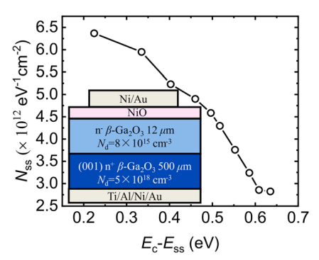
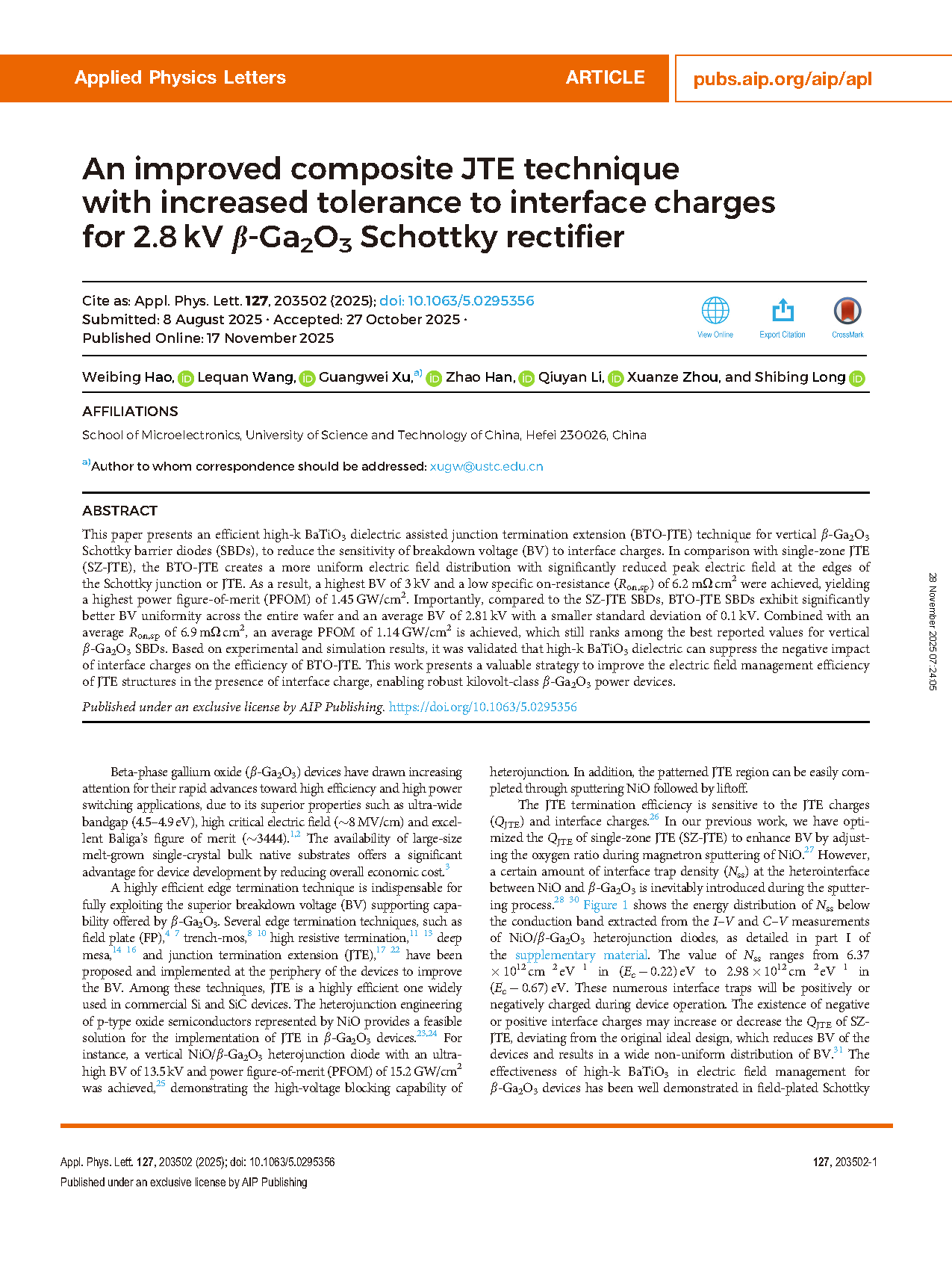
FIG. 1. Distribution profile of the interface state density as a function of interface state energy with respect to the conduction band (Ec–Ess) obtained from the measured experimental data of NiO/β-Ga2O3 heterojunction diodes.
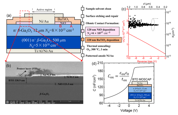
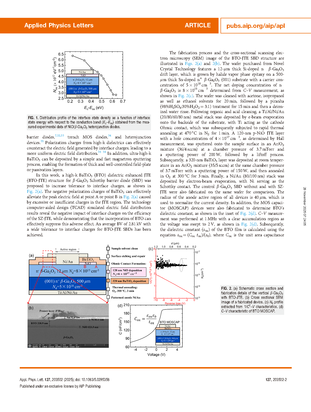
FIG. 2. (a) Schematic cross section and fabrication details of the vertical β-Ga2O3 with BTO-JTE. (b) Cross sectional SEM image of a fabricated device. (c) Nd profile extracted from 1/C2 –V characteristics. (d) C–V characteristic of BTO MOSCAP.

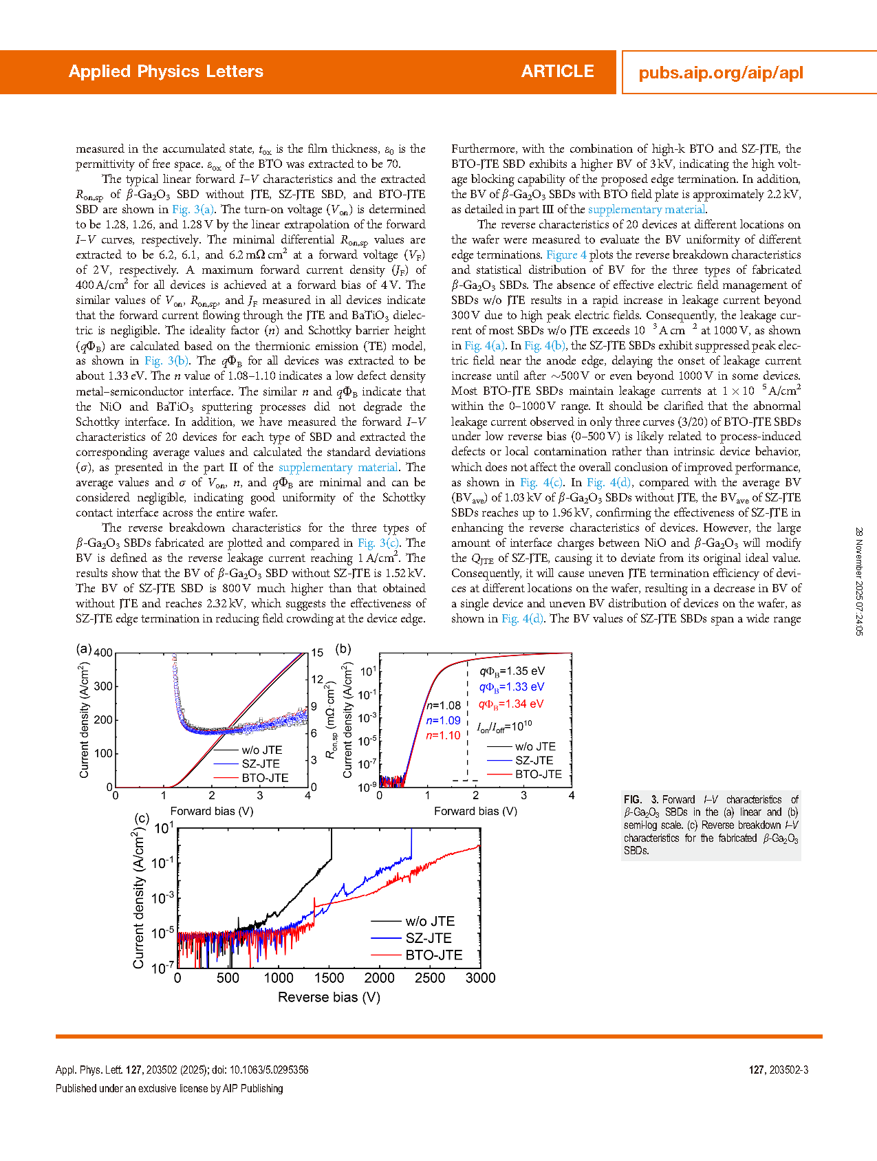
FIG. 3. Forward I–V characteristics of β-Ga2O3 SBDs in the (a) linear and (b) semi-log scale. (c) Reverse breakdown I–V characteristics for the fabricated β-Ga2O3 SBDs.
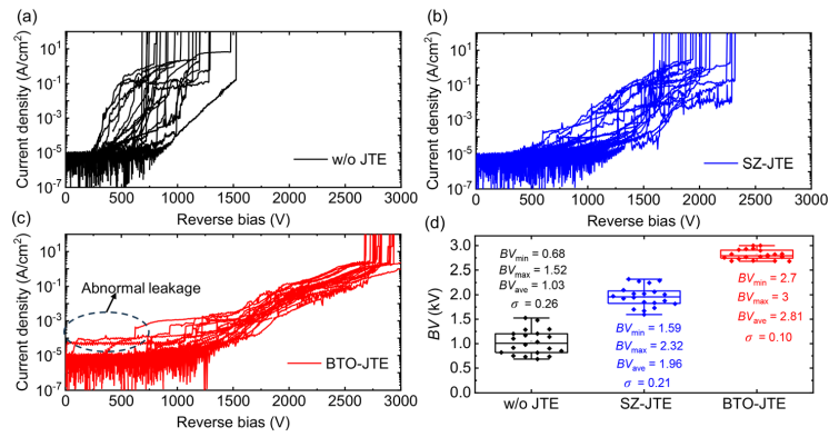
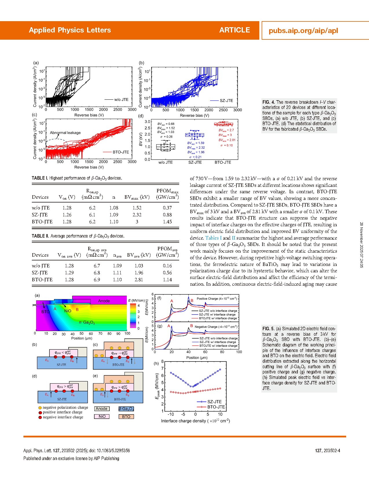
FIG. 4. The reverse breakdown I–V characteristics of 20 devices at different locations of the sample for each type β-Ga2O3 SBDs, (a) w/o JTE, (b) SZ-JTE, and (c) BTO-JTE. (d) The statistical distribution of BV for the fabricated β-Ga2O3 SBDs.
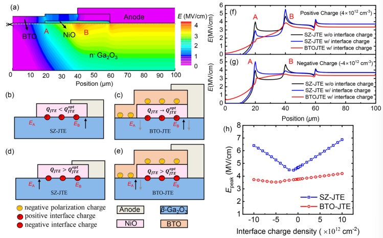
FIG. 5. (a) Simulated 2D electric field contours at a reverse bias of 3 kV for β-Ga2O3 SBD with BTO-JTE. (b)–(e) Schematic diagram of the working principle of the influence of interface charges and BTO on the electric field. Electric field distribution extracted along the horizontal cutting line of β-Ga2O3 surface with (f) positive charge and (g) negative charge. (h) Simulated peak electric field vs interface charge density for SZ-JTE and BTO-JTE.
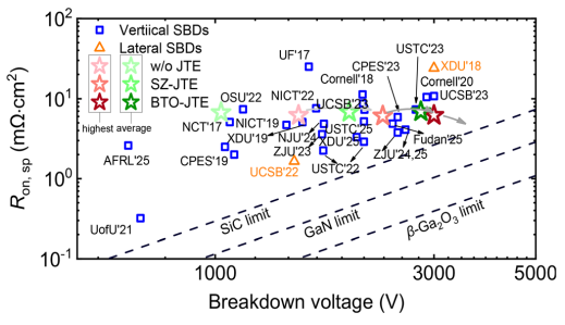
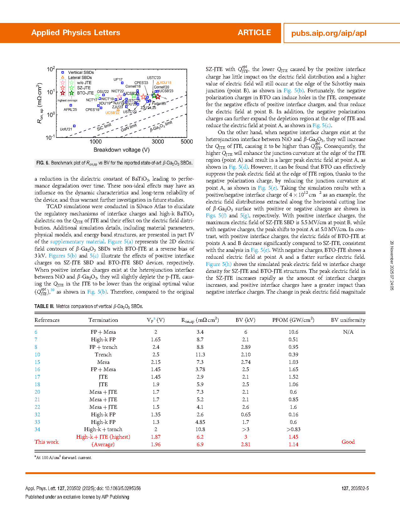
FIG. 6. Benchmark plot of Ron,sp vs BV for the reported state-of-art β-Ga2O3 SBDs.
DOI:
doi.org/10.1063/5.0295356