Paper Sharing
【Domestic Papers】Room-temperature single-photon emission from β-Ga₂O₃
日期:2025-12-05阅读:476
Researchers from the Beijing University of Technology and Chinese Academy of Sciences have published a dissertation titled " Room-temperature single-photon emission from β-Ga2O3" in Nature Communications.
Project Support
This work was partially supported by the National Natural Science Foundation of China (Grant No. 62174009, J.M. and 52473268, X.Z.) and the National Key Research and Development Program of China (Grant No. 2024YFA1409702, X.Z.).
Background
Single photon sources are key elements for various scalable quantum information technologies including quantum communication, quantum computing, quantum sensing and measurement. So far, single photon emission has been observed from various quantum emitters such as single molecules, atoms, ions, quantum dots, and point defects in semiconductors. Among them, color centers in wide bandgap semiconductors are considered to be one of the most promising single photon emitters (SPEs) due to their unique properties of stable emission at room temperature or even at high temperature as well as a wide range of single-photon emission wavelengths. Furthermore, the SPEs based on wide bandgap semiconductors are compatible with mature semiconductor technologies, which is beneficial for the integration of optoelectronic devices. In recent years, defect-based SPEs have been discovered in various wide bandgap materials, such as diamond, silicon carbide (SiC), silicon nitride (SiN), zinc oxide (ZnO), gallium nitride (GaN), aluminum nitride (AlN), and hexagonal boron nitride (h-BN).
Abstract
Single photon emitters (SPEs) hosted by the wide bandgap semiconductors have the great potential to enable quantum applications at room temperature. Recently, many defect-based SPEs have been discovered in various wide bandgap materials, such as diamond, AlN, SiC, h-BN, GaN and ZnO. Beta-phase gallium oxide (β-Ga2O3) is an emerging ultrawide bandgap semiconductor with promising electronic and optoelectronic properties, however, there has been no report on single-photon emission from β-Ga2O3 to date. Herein, we present the demonstration of room-temperature photostable single-photon emission from β-Ga2O3. We find that the SPEs can be found in a variety of β-Ga2O3 including homoepitaxial and heteroepitaxial β-Ga2O3 films and commercially available β-Ga2O3 wafers. The observed emitters have excellent photophysical characteristics including high purity, high brightness, and linear polarization. First-principles calculations predict that a localized neutral divacancy defect, generated by plasma treatment and activated by annealing, is responsible for the SPEs in β-Ga2O3. The high-performance room-temperature SPEs embedded in a technologically mature semiconductor are promising for on-chip scalable integrated devices and quantum technologies.
Conclusion
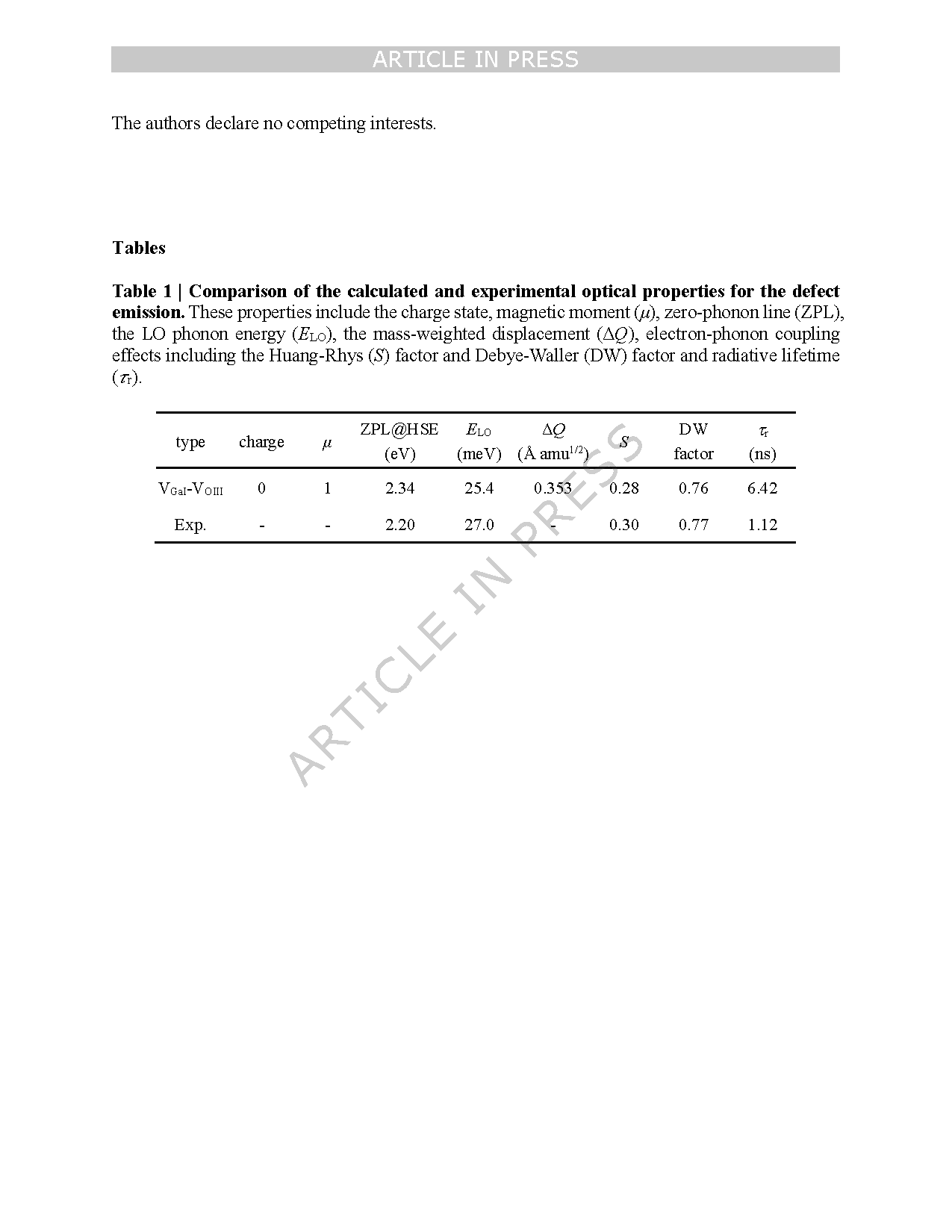
In summary, optically stable single-photon emissions from point defects in β-Ga2O3 in the visible range have been observed at room temperature. We found that the SPEs can be generated in various β-Ga2O3, including homoepitaxial and heteroepitaxial β-Ga2O3 films and commercially available single-crystal β-Ga2O3 wafers, by plasma treatment combined with annealing. Compared with the heteroepitaxial β-Ga2O3 films, the emitters hosted by homoepitaxial β-Ga2O3 films and single-crystal β-Ga2O3 wafers exhibit better performance. Photophysical analysis reveals bright (~105 counts/s after correction), pure (g2(0) < 0.2), stable, linearly polarized room-temperature quantum light emission from color centers in various β-Ga2O3 samples. DFT calculations indicate that the neutral VGaI-VOIII defect is responsible for the observed single-photon emissions. This bright SPEs operating at room temperature provides a fundamental building block for β-Ga2O3-based optoelectronic devices and future integrated quantum photonics.
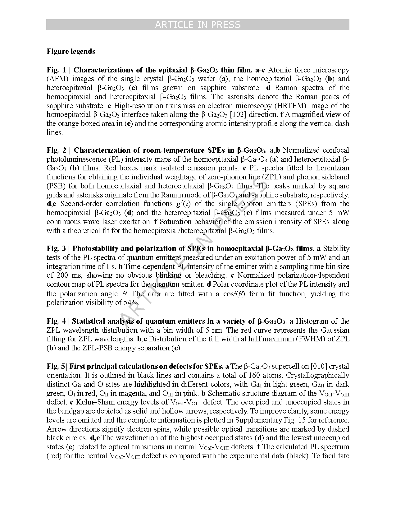
Fig. 1 | Characterizations of the epitaxial β-Ga2O3 thin film. (a-c) Atomic force microscopy (AFM) images of the single crystal β-Ga2O3 wafer (a), the homoepitaxial β-Ga2O3 (b) and heteroepitaxial β-Ga2O3 (c) films grown on sapphire substrate. (d) Raman spectra of the homoepitaxial and heteroepitaxial β-Ga2O3 films. The asterisks denote the Raman peaks of sapphire substrate. (e) High-resolution transmission electron microscopy (HRTEM) image of the homoepitaxial β-Ga2O3 interface taken along the β-Ga2O3 [102] direction. (f) A magnified view of the orange boxed area in (e) and the corresponding atomic intensity profile along the vertical dash lines.
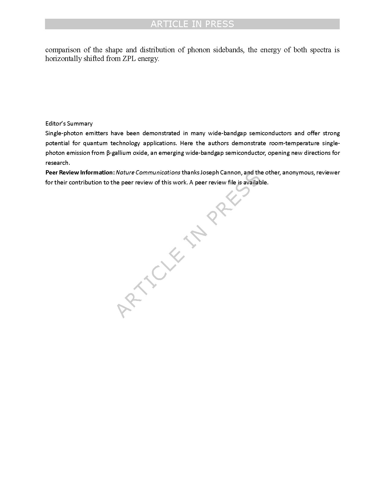
Fig. 2 | Characterization of room-temperature SPEs in β-Ga2O3. (a,b) Normalized confocal photoluminescence (PL) intensity maps of the homoepitaxial β-Ga2O3 (a) and heteroepitaxial β-Ga2O3 (b) films. Red boxes mark isolated emission points. (c) PL spectra fitted to Lorentzian functions for obtaining the individual weightage of zero-phonon line (ZPL) and phonon sideband (PSB) for both homoepitaxial and heteroepitaxial β-Ga2O3 films. The peaks marked by square grids and asterisks originate from the Raman mode of β-Ga2O3 and sapphire substrate, respectively. (d,e) Second-order correlation functions g2(τ) of the single photon emitters (SPEs) from the homoepitaxial β-Ga2O3 (d) and the heteroepitaxial β-Ga2O3 (e) films measured under 5 mW continuous wave laser excitation. (f) Saturation behavior of the emission intensity of SPEs along with a theoretical fit for the homoepitaxial/heteroepitaxial β-Ga2O3 films.
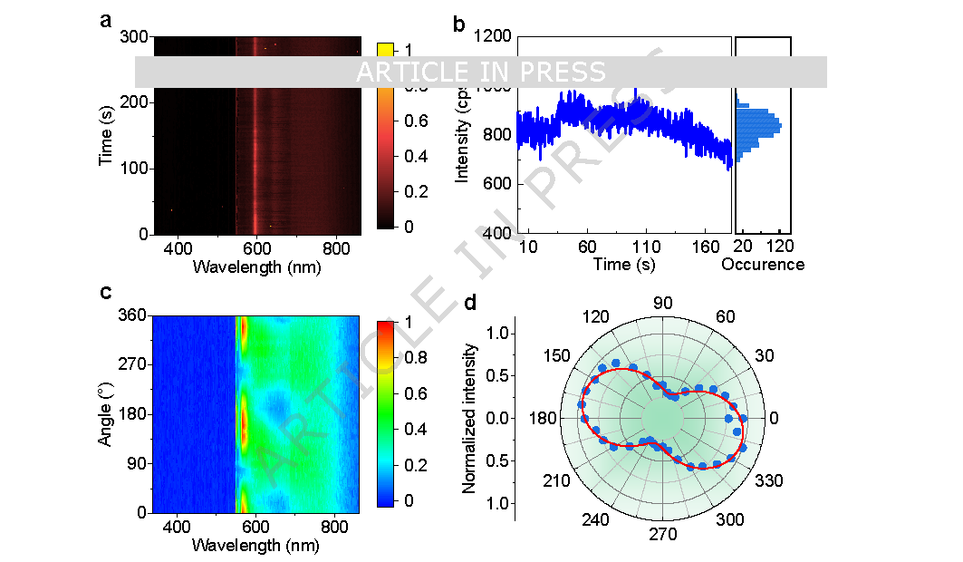
Fig. 3 | Photostability and polarization of SPEs in homoepitaxial β-Ga2O3 films. a Stability tests of the PL spectra of quantum emitters measured under an excitation power of 5 mW and an integration time of 1 s. b Time-dependent PL intensity of the emitter with a sampling time bin size of 200 ms, showing no obvious blinking or bleaching. c Normalized polarization-dependent contour map of PL spectra for the quantum emitter. d Polar coordinate plot of the PL intensity and the polarization angle q. The data are fitted with a cos2(θ) form fit function, yielding the polarization visibility of 54%.
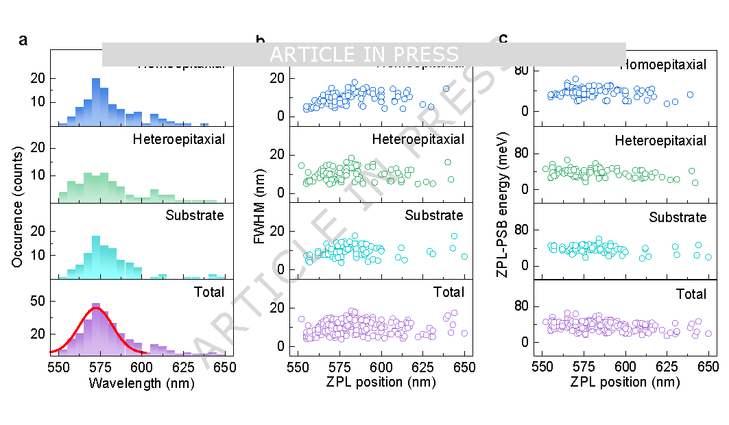
Fig. 4 | Statistical analysis of quantum emitters in a variety of β-Ga2O3. (a) Histogram of the ZPL wavelength distribution with a bin width of 5 nm. The red curve represents the Gaussian fitting for ZPL wavelengths. (b,c) Distribution of the full width at half maximum (FWHM) of ZPL (b) and the ZPL-PSB energy separation (c).
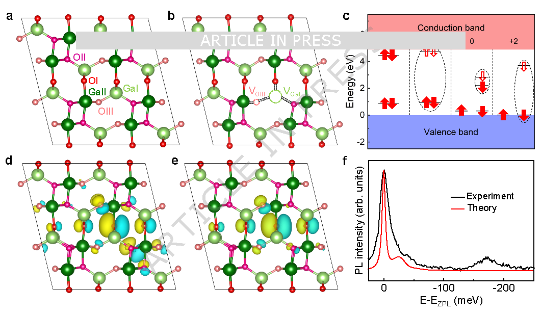
Fig. 5 | First principal calculations on defects for SPEs. (a) The β-Ga2O3 supercell on [010] crystal orientation. It is outlined in black lines and contains a total of 160 atoms. Crystallographically distinct Ga and O sites are highlighted in different colors, with GaΙ in light green, GaΙΙ in dark green, OΙ in red, OΙΙ in magenta, and OΙΙΙ in pink. (b) Schematic structure diagram of the VGaI-VOIII defect. (c) Kohn–Sham energy levels of VGaI-VOIII defect. The occupied and unoccupied states in the bandgap are depicted as solid and hollow arrows, respectively. To improve clarity, some energy levels are omitted and the complete information is plotted in Supplementary Fig. 15 for reference. Arrow directions signify electron spins, while possible optical transitions are marked by dashed black circles. (d,e) The wavefunction of the highest occupied states (d) and the lowest unoccupied states (e) related to optical transitions in neutral VGaI-VOIII defects. (f) The calculated PL spectrum (red) for the neutral VGaI-VOIII defect is compared with the experimental data (black). To facilitate comparison of the shape and distribution of phonon sidebands, the energy of both spectra is horizontally shifted from ZPL energy.
DOI:
doi.org/10.1038/s41467-025-66953-9