Paper Sharing
【Member Papers】Fermi-Level Pinning-Free 2D Hybrid MXene/β-Ga₂O₃ van der Waals Polarization-Sensitive Schottky Photodiodes
日期:2025-12-05阅读:457
Researchers from the Nanjing University of Posts and Telecommunications have published a dissertation titled "Fermi-Level Pinning-Free 2D Hybrid MXene/β-Ga2O3 van der Waals Polarization-Sensitive Schottky Photodiodes" in Laser & Photonics Reviews.
Project Support
This work was supported by the Joint Funds of the National Natural Science Foundation of China (Grant No. U23A20349), the National Natural Science Foundation of China (Grant Nos. 62204125, 62305171, 62564011 and 62501320), the Key Technology Project of Suzhou City (Grant No. SYG2024003), the Jiangsu Provincial Team of Innovation and Entrepreneurship (Grant No. JSSCTD202351), the Program for Innovative Research Team in Universities of Inner Mongolia Autonomous Region (Grant No. NMGIRT2503), the Inner Mongolia Autonomous Region-level Scientific Research Startup Fund (Grant Nos. 21700-252904 and 21700- 252905), the Steed Plan of Inner Mongolia University for Introducing High-Level Talents (Grant Nos. 10000-A24199006 and 10000-A24106015), and the Inner Mongolia University Experimental Technology Research Project in 2025 (Self-Made and Modified Equipment Project) (Grant No. SYJS2025004).
Background
Deep ultraviolet (DUV) photodiodes are essential components in modern solid-state optoelectronic systems, capable of converting DUV light (<280 nm) into electrical signals. This functionality makes them highly valuable for various applications, including deep space exploration, environmental monitoring, and the Internet of Things (IoT). Lasting for decades, the polarized photodetector, a new type of photoelectric device, has been a significant concern due to its unique application prospects in medical and health fields. Recent research has focused on identifying suitable materials for DUV detection to meet the evolving demands of modern electronics. In recent years, 2D materials have emerged as a highly promising class of materials, garnering significant attention within the field of photodetectors due to their remarkable properties.
Abstract
Metal-semiconductor (MS) interface plays a crucial role in electronic and optoelectronic devices, where Fermi-level (FL) pinning is the primary proposal for the formation of a Schottky barrier. The concerned carrier transport would be seriously influenced by the electronic states and defects at the MS interface. Traditional metal electrodes always introduce a severe FL pinning effect, which limits device performance. Thus, introducing an MS interface with low contact resistance and weak FL pinning is desired. Here, a high-performance MXene/β-Ga2O3 van der Waals (vdW) Schottky photodiode is introduced. The exceptional MXene/β-Ga2O3 interface alleviates FL pinning by achieving a pinning factor of 0.995, remarkably close to the Schottky-Mott limit. In this case, the rectification ratio of MXene/β-Ga2O3 vdW Schottky photodiode approaches ∼109 with an ultra-low reverse leak current of ∼10−12 A. The proposed photodiode exhibits standout self-powered photoresponse, its rise and decay times are 0.27 and 0.29 ms, respectively, and responsivity is 125.1 mA/W. Notably, the device exhibits polarization-sensitive photodetection with a linear dichroic ratio of 7.1 at zero bias. These findings underscore the promise of MXene/β-Ga2O3 vdW Schottky photodiode for next-generation deep ultraviolet (DUV) optoelectronic technologies, offering superior performance and potential applications in the Internet of Things and energy-efficient systems.
Conclusions
In summary, we proposed Ti3C2TX/β-Ga2O3 vdW Schottky photodiodes, addressing the long-standing challenge of the FL pinning effect in MS contacts. The Dit for the Ti3C2TX vdW contacts with β-Ga2O3 is approximately 10 times lower than that of Ni contacts with β-Ga2O3. And the S of our proposed device is approaching the Schottky–Mott limit. This critical improvement translates into a substantially faster response speed, enabling the device to operate with heightened efficiency and precision in dynamic scenarios. Beyond its enhanced speed, the device demonstrates exceptional capabilities in the realm of deep-ultraviolet polarized light detection. Furthermore, it successfully realizes high-quality deep UV polarized light detection imaging. What’s more, the device, with its comprehensive set of advanced features and reliable performance, is fully capable of meeting the stringent and evolving requirements of modern artificial intelligence systems. Its ability to process information rapidly, detect specialized light signals with precision, and generate clear imaging data makes way in the next generation of artificial intelligence technologies.

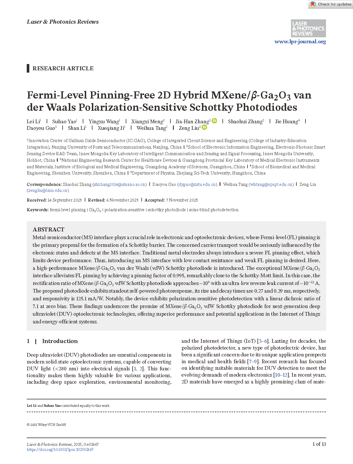
FIGURE 1 (a) XRD of the β-Ga2O3. (b) FWHM of XRD of the β-Ga2O3. (c) The HR-TEM of the β-Ga2O3. (d) Surface characterization and thickness (inset) of the Ti3C2Tx film. (e) TEM of the interface of Ti3C2Tx and β-Ga2O3. (f) The EDS elements mapping of Ti and Ga.
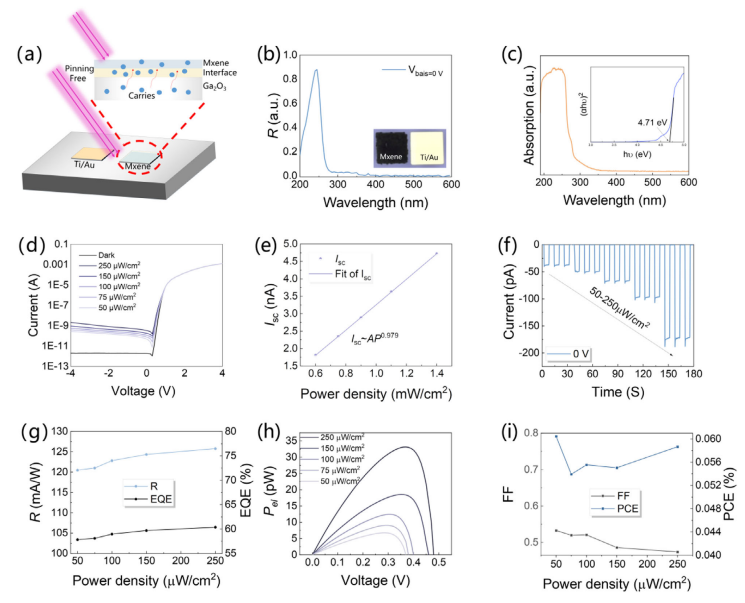
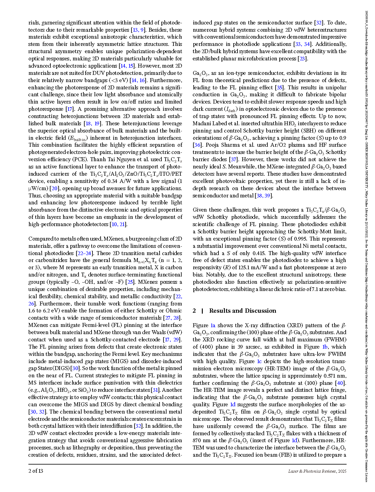
FIGURE 2 (a) schematic diagram of the Ti3C2TX/β-Ga2O3 vdW Schottky photodiodes. (b) The photoresponse spectrum of the photodiode, and the inset is the individual complete device. (c) absorbance spectrum of the β-Ga2O3, and the inset is the corresponding tauc plot. (d) The I–V curve of the proposed photodiode. (e) Extracted the Isc and light density of the photodiode. (f) I-t curve of the photodiode at 0 V. (g) The R and EQE of the proposed photodiode. (h) pel under 255 nm light illuminated with different densities. (i) ff and pec of the proposed photodiode.
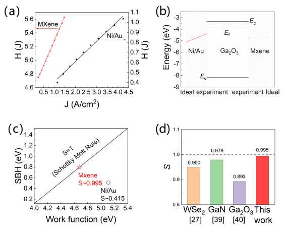
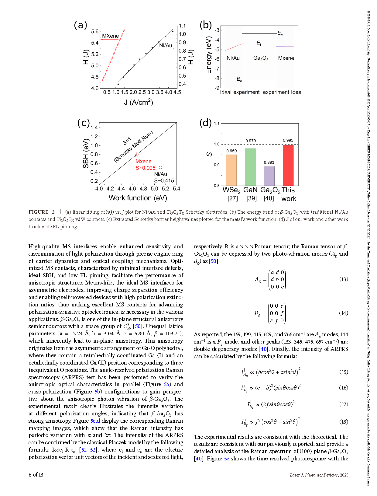
FIGURE 3 (a) linear fitting of h(j) vs. j plot for Ni/Au and Ti3C2TX Schottky electrodes. (b) The energy band of β-Ga2O3 with traditional Ni/Au contacts and Ti3C2TX vdW contacts. (c) Extracted Schottky barrier height values plotted for the metal’s work function. (d) S of our work and other work to alleviate FL pinning.

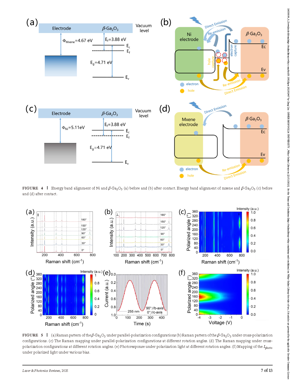
FIGURE 4 Energy band alignment of Ni and β-Ga2O3 (a) before and (b) after contact. Energy band alignment of mxene and β-Ga2O3 (c) before and (d) after contact.
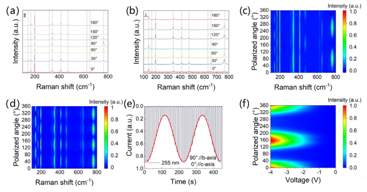
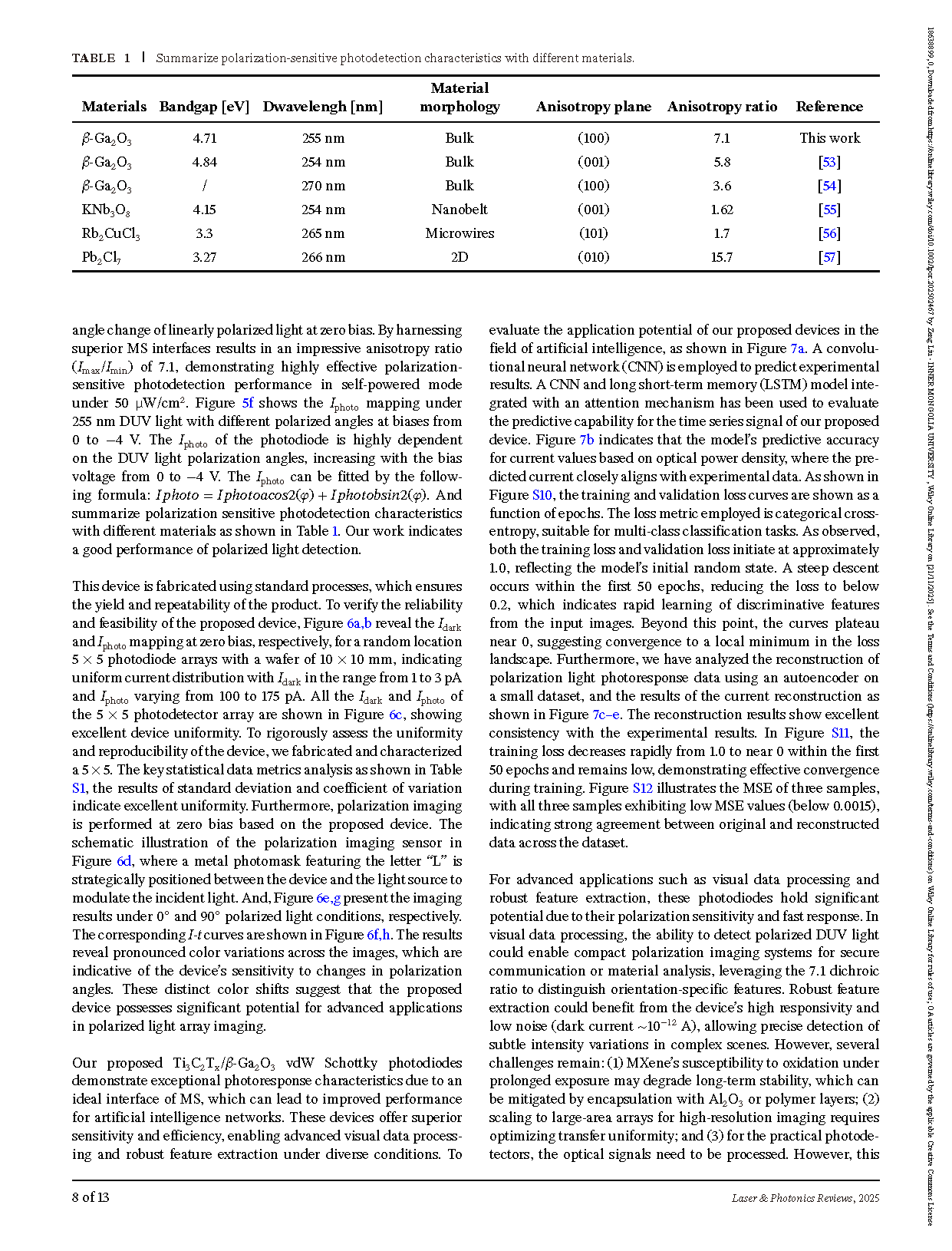
FIGURE 5 (a) Raman pattern of the β-Ga2O3 under parallel-polarization configurations (b) Raman pattern of the β-Ga2O3 under cross-polarization configurations. (c) The Raman mapping under parallel-polarization configurations at different rotation angles. (d) The Raman mapping under cross-polarization configurations at different rotation angles. (e) Photoresponse under polarization light at different rotation angles. (f) Mapping of the Iphoto under polarized light under various bias.
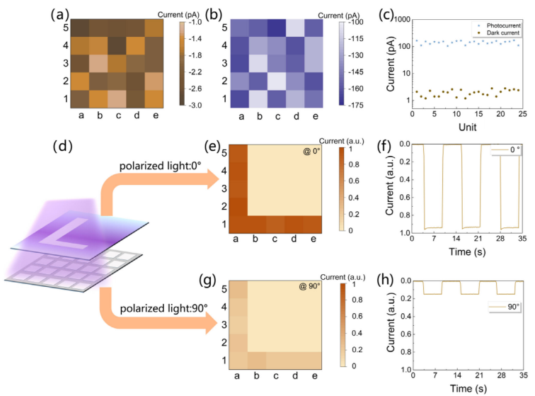
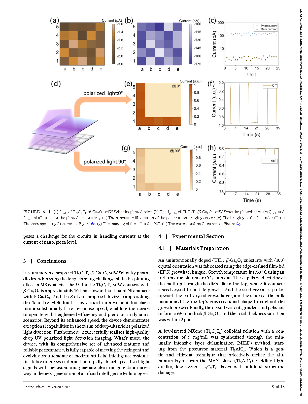
FIGURE 6 (a) Idark of Ti3C2TX/β-Ga2O3 vdW Schottky photodiodes. (b) The Iphoto of Ti3C2TX/β-Ga2O3 vdW Schottky photodiodes. (c) Idark and Iphoto of all units for the photodetector array. (d) The schematic illustration of the polarization imaging sensor. (e) The imaging of the “l” under 0◦. (f) The corresponding I-t curves of Figure 6e. (g) The imaging of the “l” under 90◦. (h) The corresponding I-t curves of Figure 6g.
DOI:
doi.org/10.1002/lpor.202502467