Paper Sharing
【Member Papers】A Pathway to High-Quality Heteroepitaxial Ga₂O₃ Films via Metalorganic Chemical Vapor Deposition
日期:2025-12-04阅读:453
Researchers from the Xidian University have published a dissertation titled "A Pathway to High-Quality Heteroepitaxial Ga2O3 Films via Metalorganic Chemical Vapor Depositionx" in Micromachines.
Project Support
This research was funded by National Natural Science Foundation of China (Grant No. 62174127), National Key Research and Development Program (Grant No. 2021YFB3601102), Key Research and Development Program of Jiangsu Province (Grant No. BE2020004-4), Shanxi Province Key Research and Development Program (Grant No. 202202030201001). We would also like to thank the Hefei Comprehensive National Science Center and Jiangsu Institute of Advanced Semiconductors Co. Ltd. And The APC was funded by Xidian University.
Background
Beta-gallium oxide (β-Ga2O3) is an emerging ultra-wide-bandgap (~4.9 eV) semiconductor with a high critical electric field (~8 MV/cm) and excellent thermal and chemical stability. These properties make it a promising candidate for high-power electronic devices, solar-blind photodetectors, and extreme-environment applications. However, the development of β-Ga2O3-based technology is hampered by the high cost and small wafer size of commercially available native substrates, driving significant interest in heteroepitaxial growth on compatible foreign substrates.
Heteroepitaxy of β-Ga2O3, however, faces fundamental challenges, primarily due to laice and thermal expansion mismatch between the film and substrate. These mismatches often lead to high defect densities, residual stress, and degraded electronic performance. In particular, oxygen vacancies—the dominant native point defect in β-Ga2O3— play a decisive role in controlling electrical conductivity, affecting device performance and stability. Therefore, understanding and controlling the formation of oxygen vacancies during heteroepitaxy is crucial for tailoring the material’s electronic properties.
Abstract
This work systematically investigates the heteroepitaxial growth of β-Ga2O3 thin films under varied substrate and temperature conditions via metalorganic chemical vapor deposition (MOCVD). Comprehensive characterization reveals that both the substrate type and growth temperature significantly influence the crystalline quality, surface morphology, chemical composition, and defect structure. Films grown at higher temperatures generally exhibit superior crystallinity and closer-to-stoichiometry composition, and thus suggest a reduction in oxygen deficiency. Certain substrates are shown to facilitate high-quality epitaxial growth with smooth surfaces and excellent crystallographic alignment. These findings offer key insights into optimizing growth parameters for high-performance β-Ga2O3-based devices.
Conclusions
In summary, this study identifies 800 °C as the optimal growth temperature for high-quality β-Ga2O3 heteroepitaxy, yielding superior crystallinity, improved stoichiometry (closer to the ideal O/Ga ratio of 3:2), and a reduced oxygen deficiency. The 6° off-cut sapphire and AlN/sapphire substrates are the most favorable, effectively mitigating non-stoichiometry and defect formation. A key finding is that surface smoothness can be misleading, as it does not guarantee high phase purity or controlled oxygen deficiency, exemplified by the p-GaN substrate. These results provide clear guidelines for optimizing chemical composition and defect control in β-Ga2O3 device fabrication.
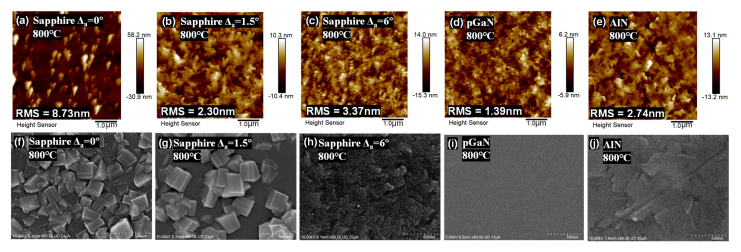
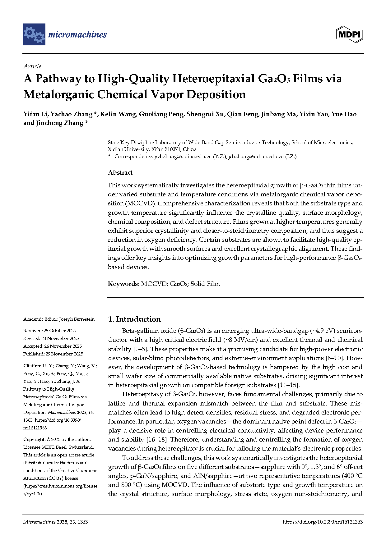
Figure 1. Surface morphology of β-Ga2O3 films heteroepitaxially grown on various substrates at 800 °C: (a–e) AFM top-view images (5 × 5 µm scan areas), and (f–j) corresponding SEM images (scale bar: 500 nm).
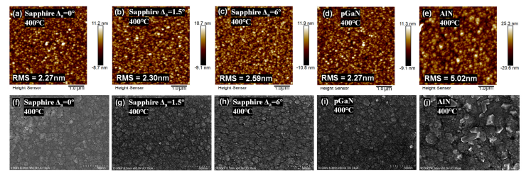
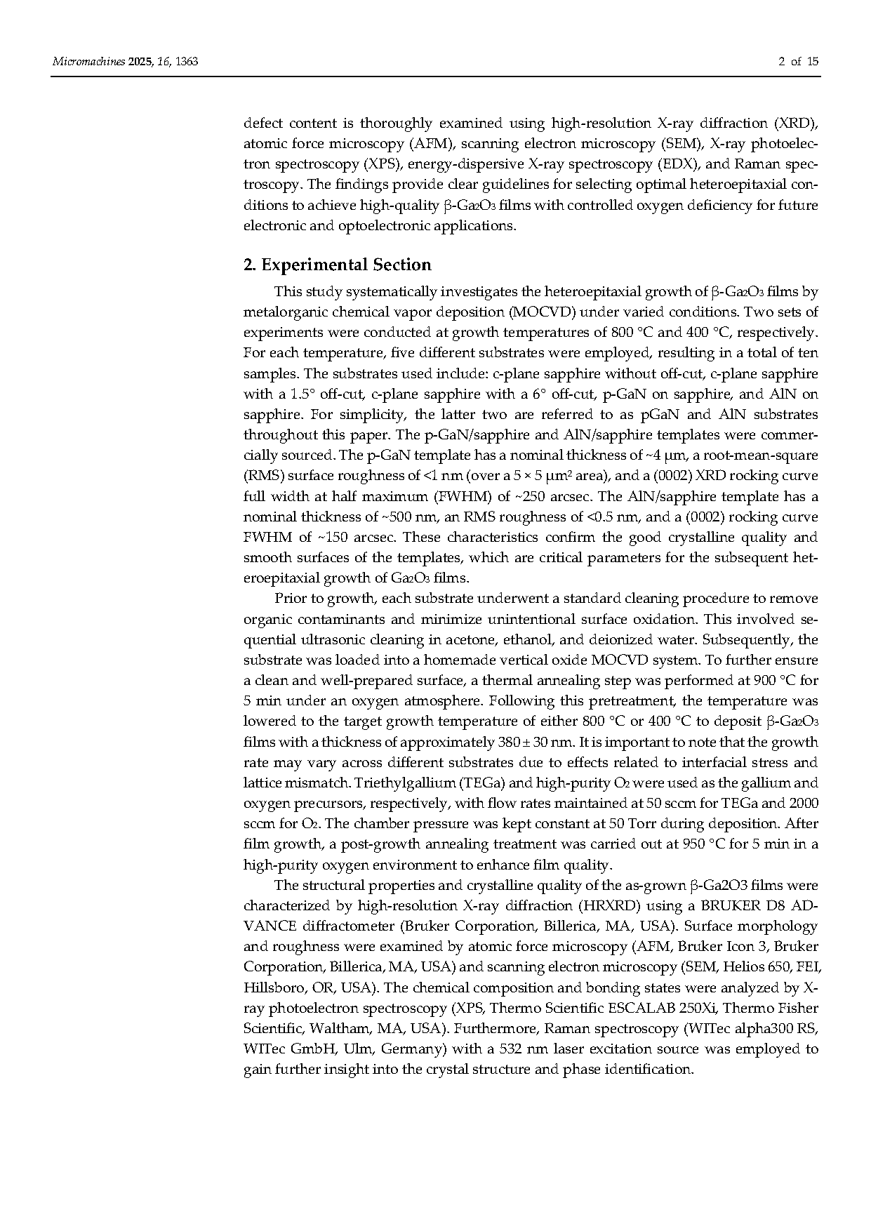
Figure 2. Surface morphology of β-Ga2O3 films heteroepitaxially grown on various substrates at 400 °C: (a–e) AFM top-view images (5 × 5 µm scan areas), and (f–j) corresponding SEM images (scale bar: 500 nm).
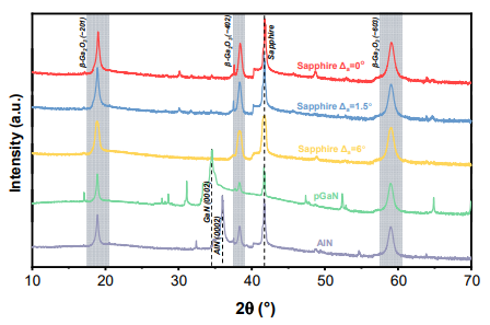
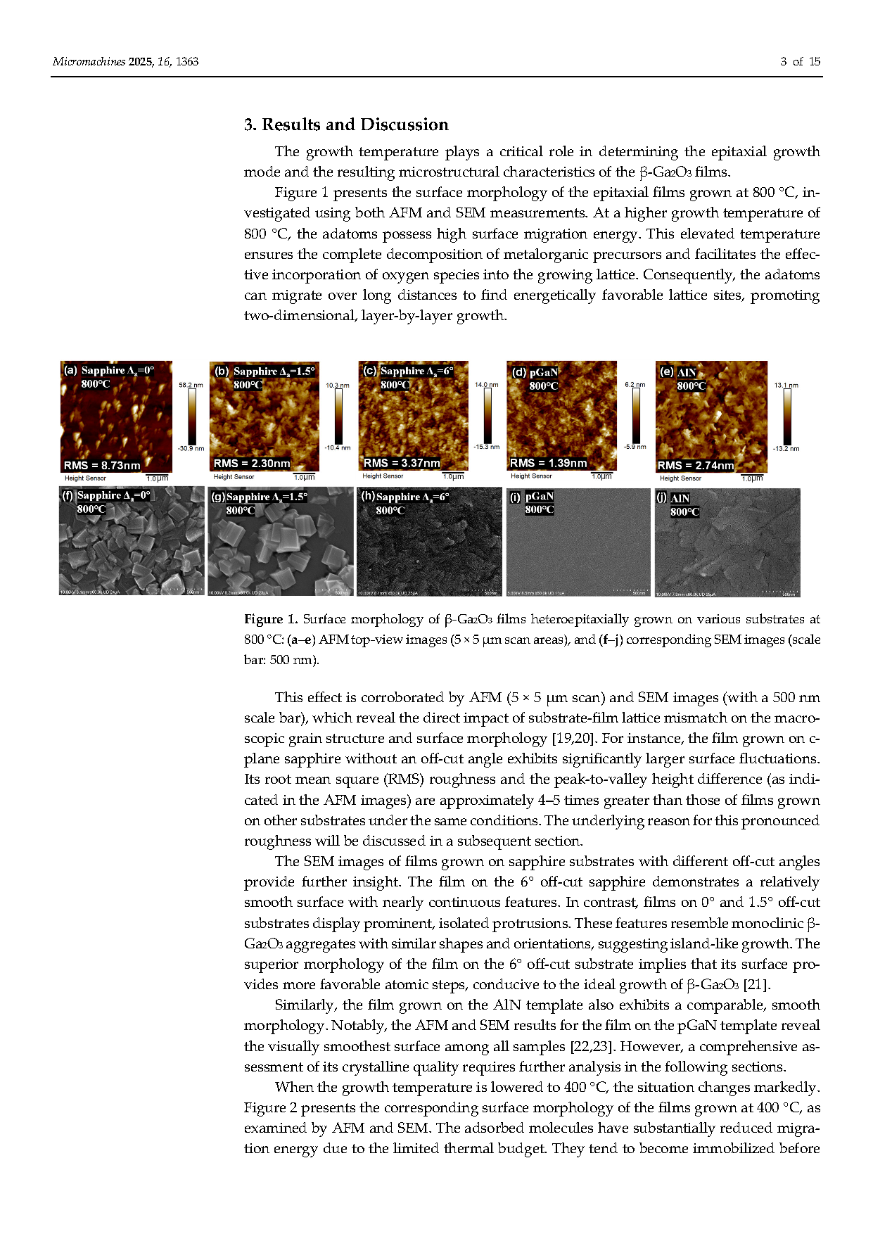
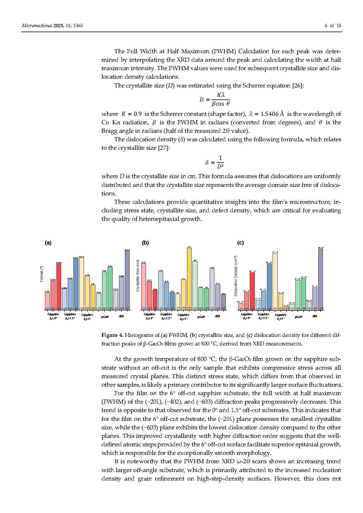
Figure 3. XRD ω-2θ scans of β-Ga2O3 films grown on different substrates at 800 °C.
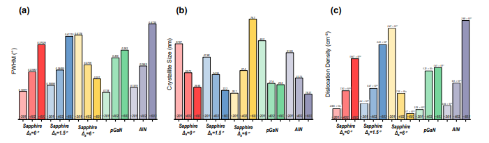
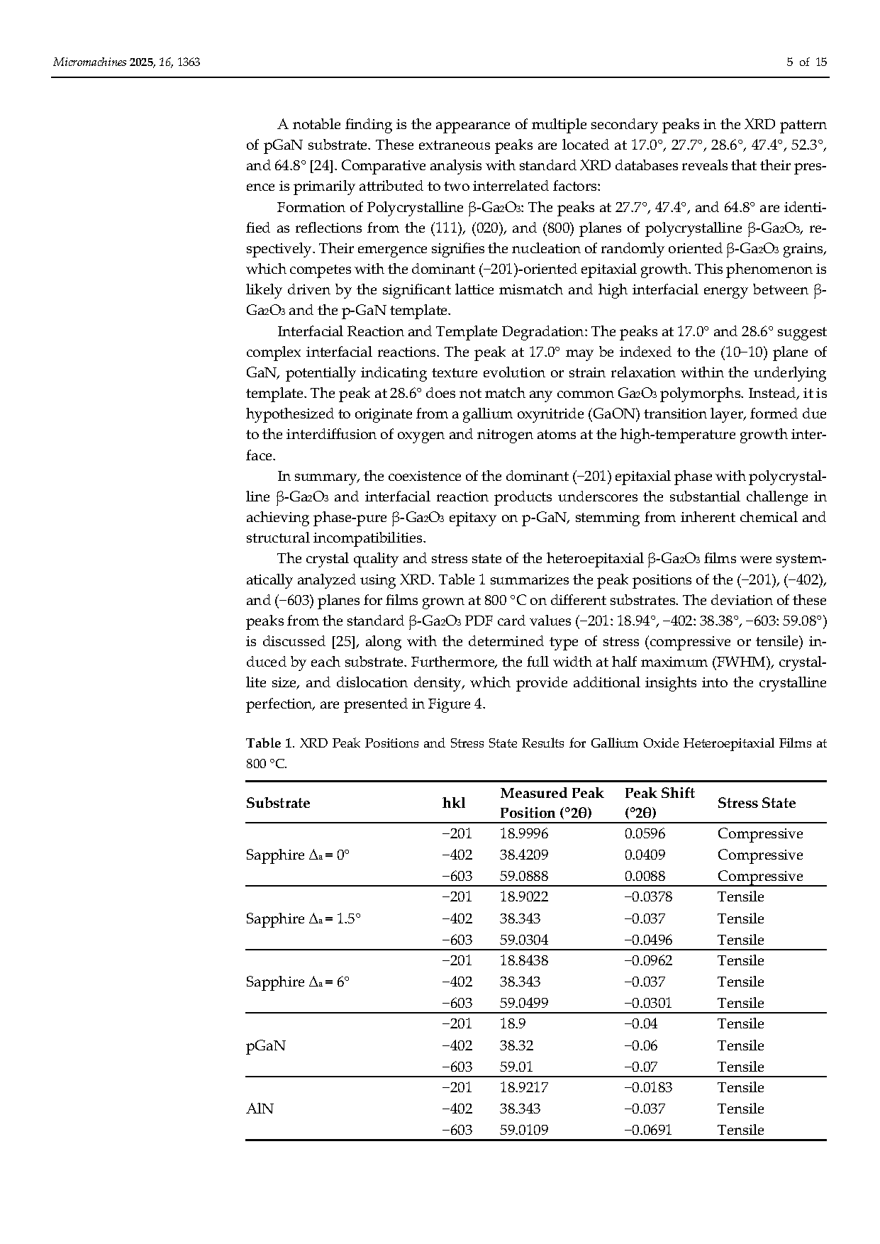
Figure 4. Histograms of (a) FWHM, (b) crystallite size, and (c) dislocation density for different diffraction peaks of β-Ga2O3 films grown at 800 °C, derived from XRD measurements.
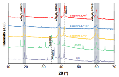
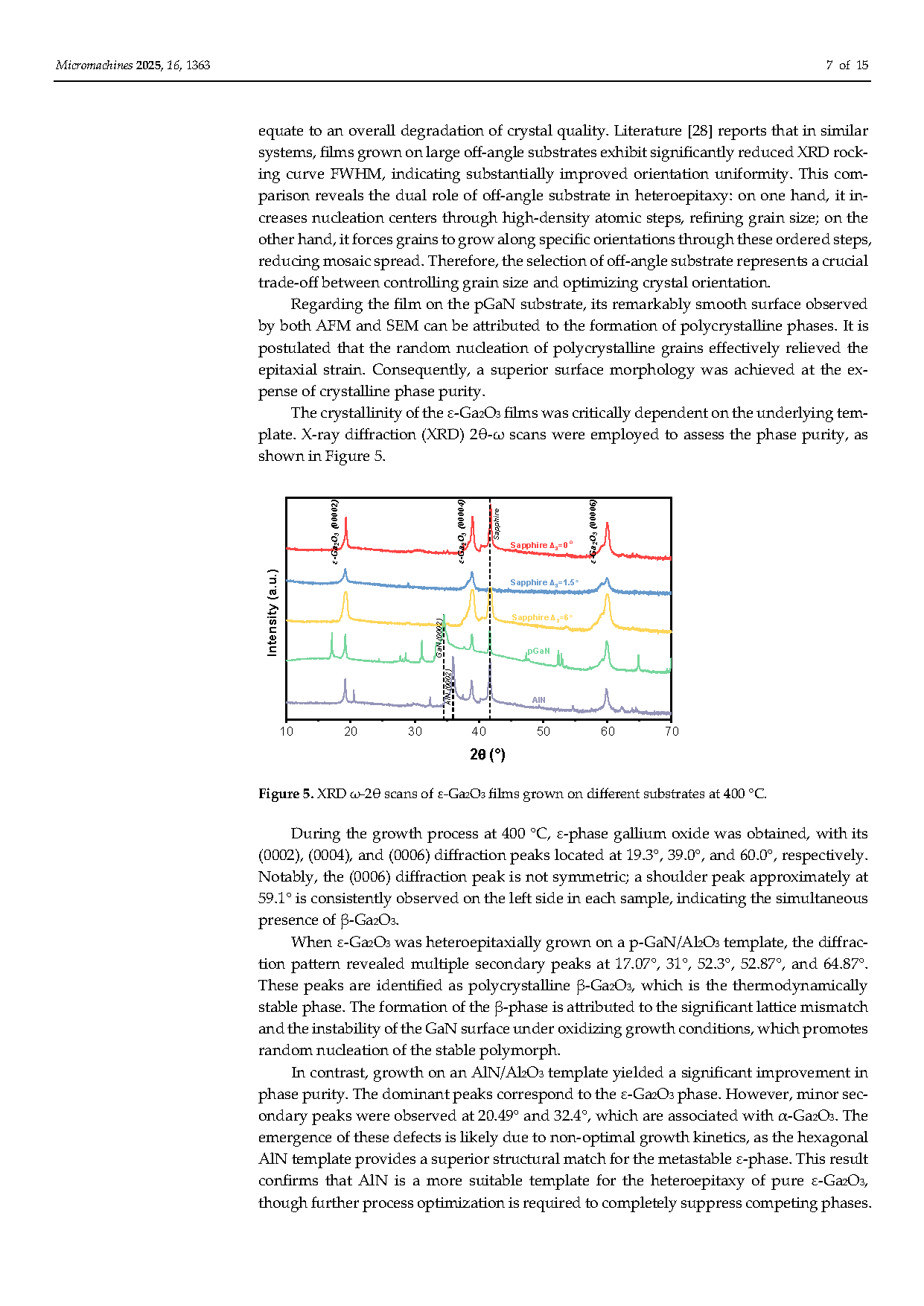
Figure 5. XRD ω-2θ scans of ε-Ga2O3 films grown on different substrates at 400 °C.
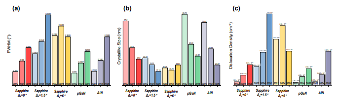
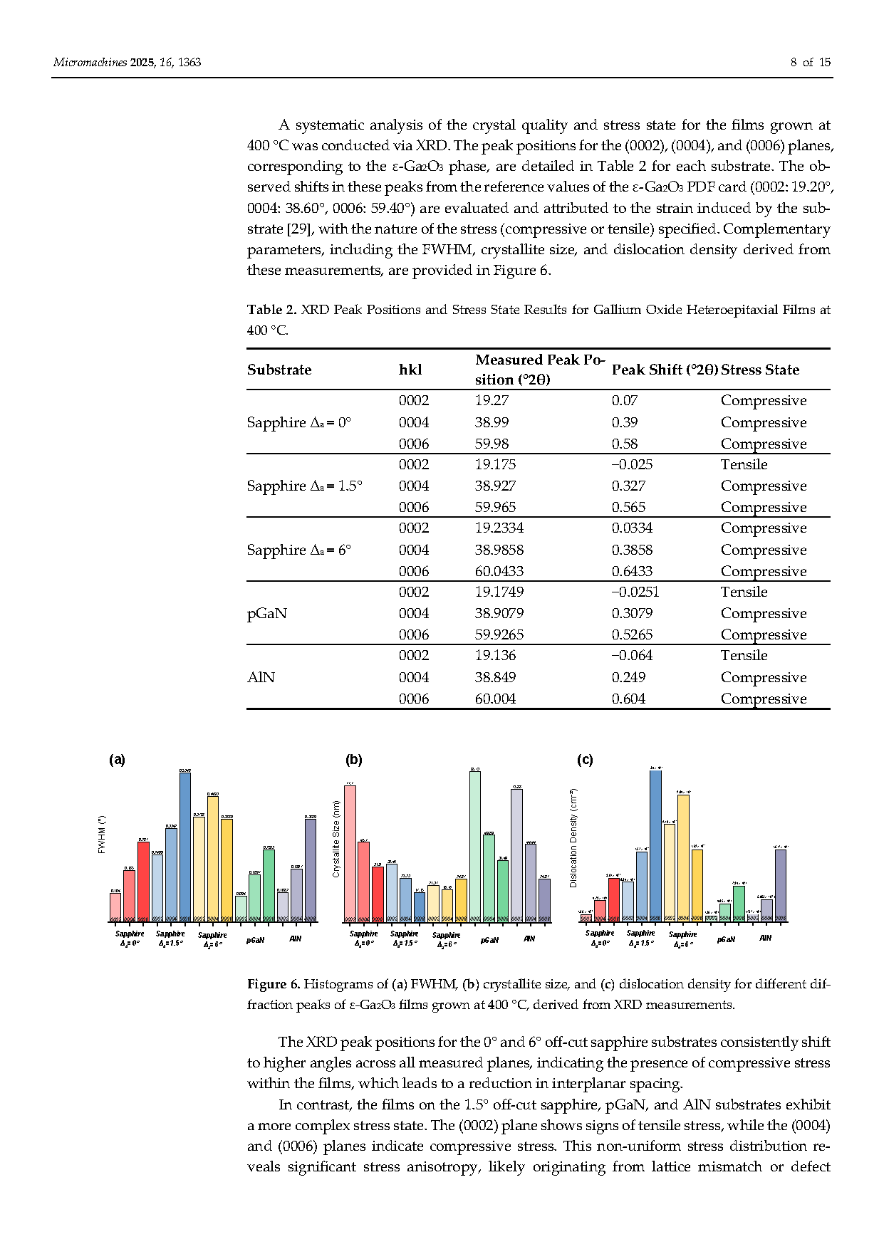
Figure 6. Histograms of (a) FWHM, (b) crystallite size, and (c) dislocation density for different diffraction peaks of ε-Ga2O3 films grown at 400 °C, derived from XRD measurements.
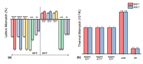
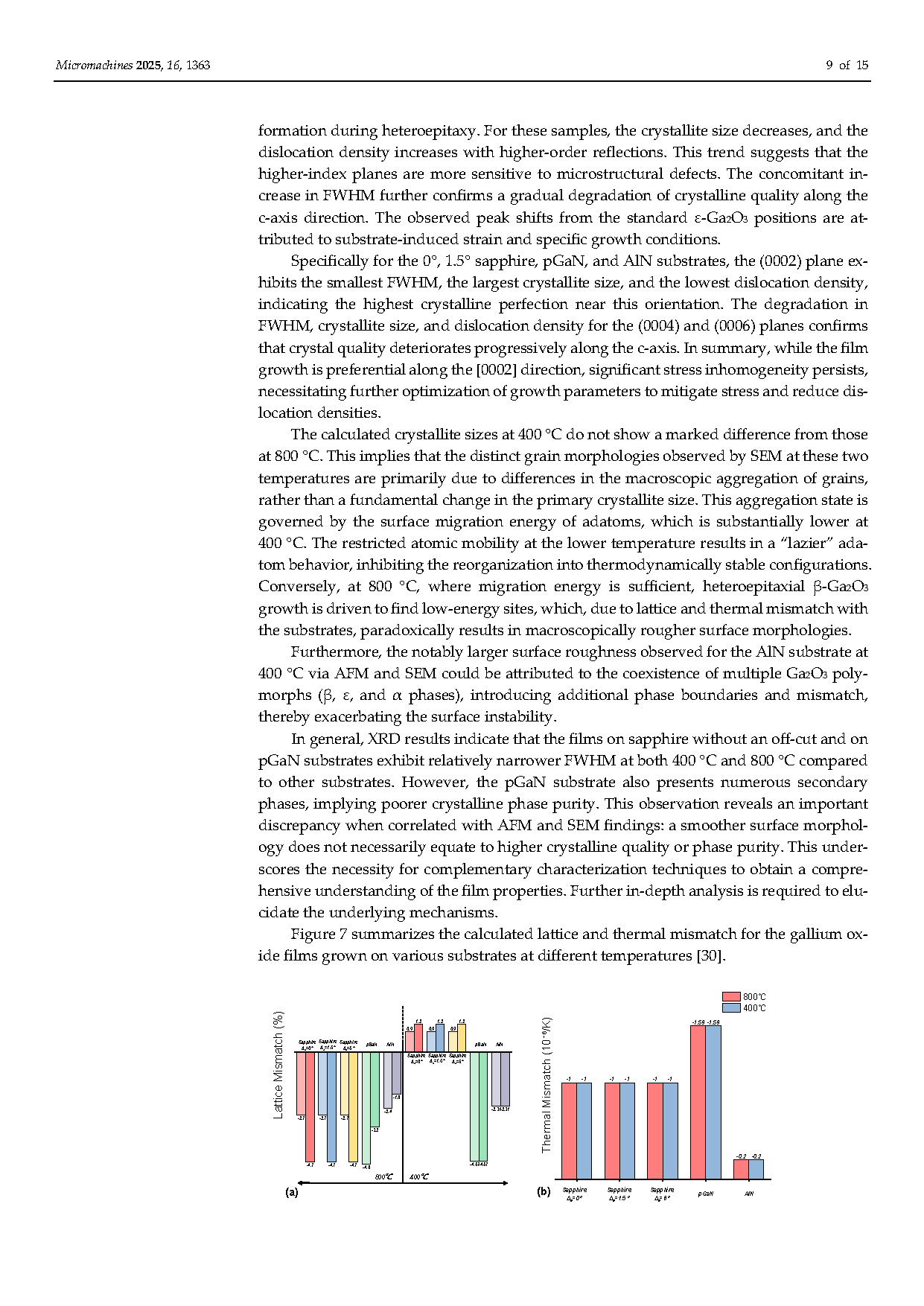
Figure 7. Histograms illustrating the (a) laice mismatch and (b) thermal mismatch between the heteroepitaxial gallium oxide films and various substrates.
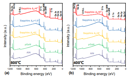
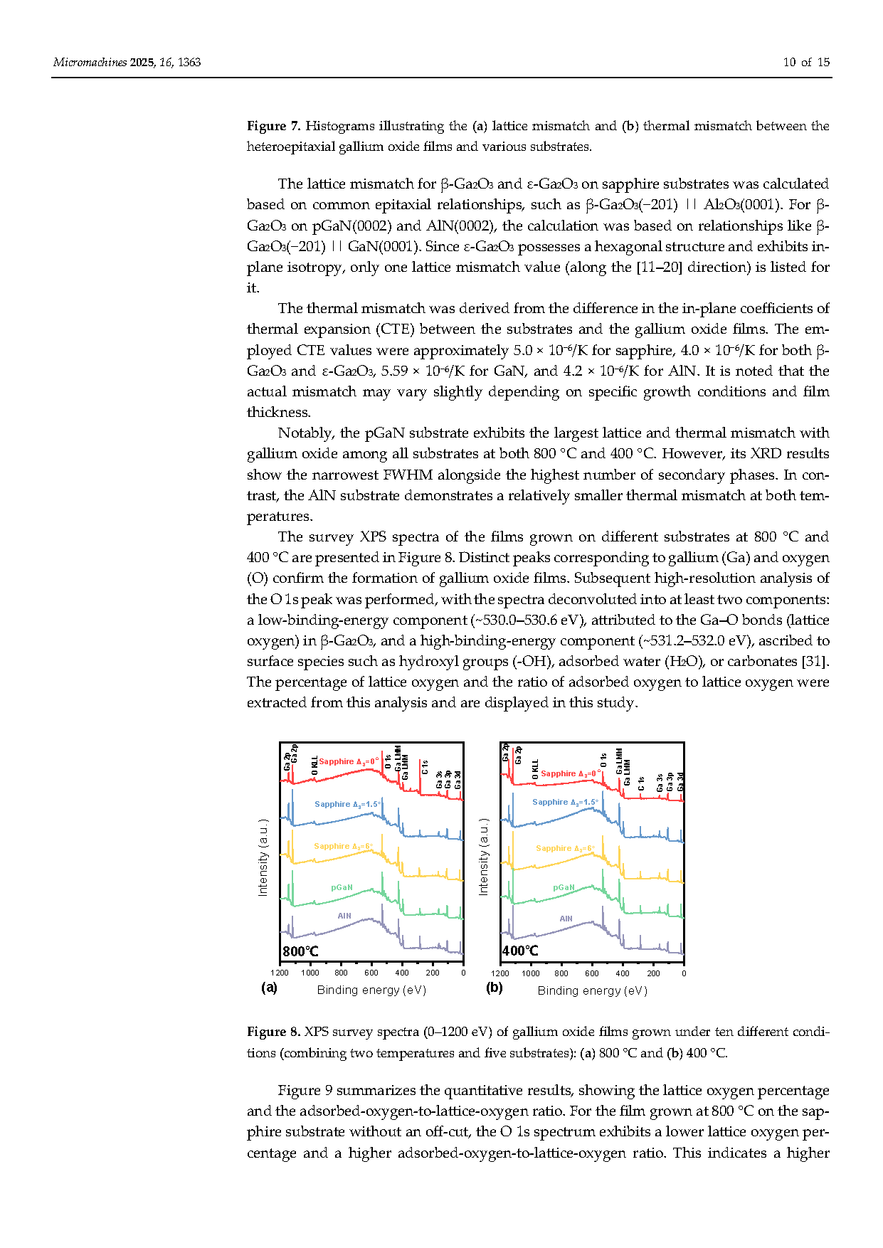
Figure 8. XPS survey spectra (0–1200 eV) of gallium oxide films grown under ten different conditions (combining two temperatures and five substrates): (a) 800 °C and (b) 400 °C.
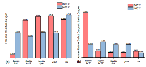
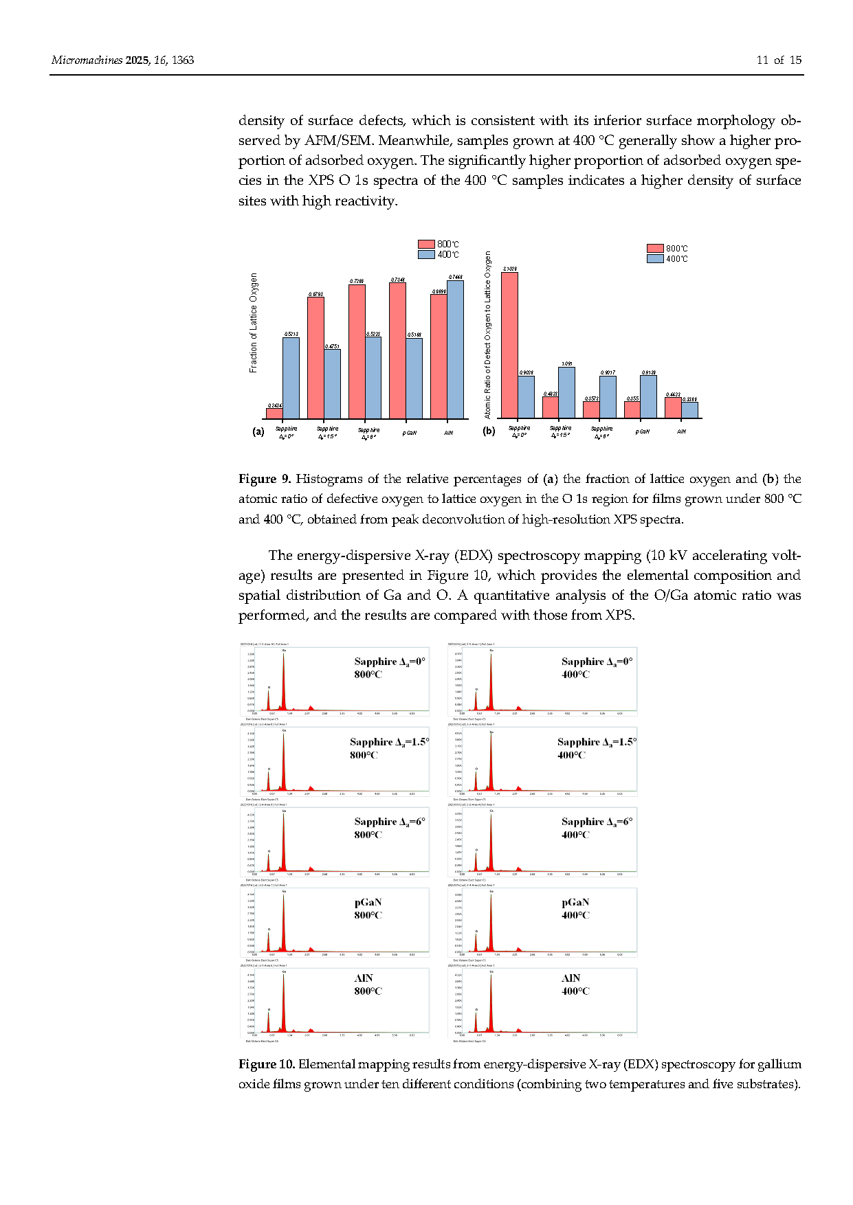
Figure 9. Histograms of the relative percentages of (a) the fraction of laice oxygen and (b) the atomic ratio of defective oxygen to laice oxygen in the O 1s region for films grown under 800 °C and 400 °C, obtained from peak deconvolution of high-resolution XPS spectra.
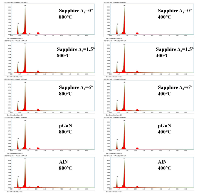
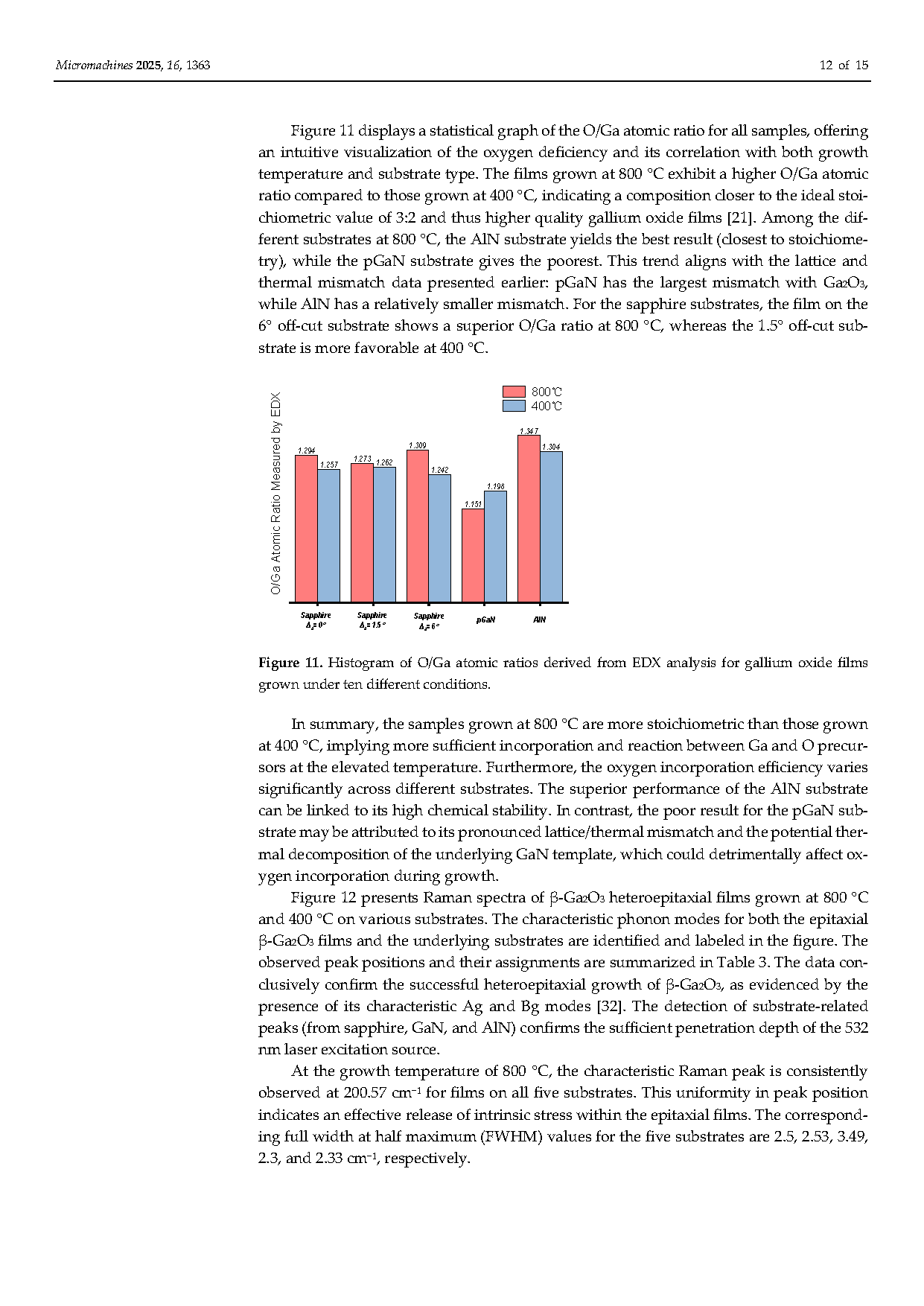
Figure 10. Elemental mapping results from energy-dispersive X-ray (EDX) spectroscopy for gallium oxide films grown under ten different conditions (combining two temperatures and five substrates).
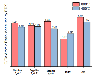
Figure 11. Histogram of O/Ga atomic ratios derived from EDX analysis for gallium oxide films grown under ten different conditions.
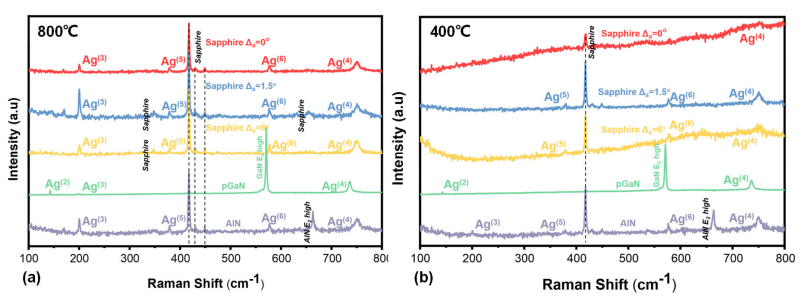
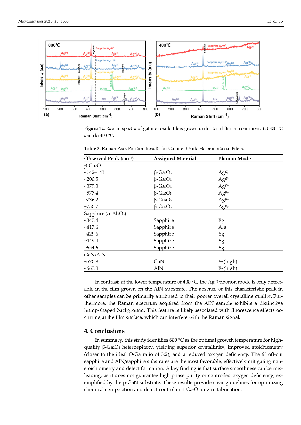
Figure 12. Raman spectra of gallium oxide films grown under ten different conditions: (a) 800 °C and (b) 400 °C.
DOI:
doi.org/10.3390/mi16121363