Paper Sharing
【Member Papers】Dual Modulation of Dark Carrier and Photocarrier in Ga₂O₃ Nanopillar Arrays for High-Performance Solar-Blind Ultraviolet Photodetectors
日期:2025-12-04阅读:427
The research team from Beijing University of Posts and Telecommunications (BUPT) and Nanjing University of Posts and Telecommunications (NJUPT) has published a paper in Laser & Photonics Reviews titled “Dual Modulation of Dark Carrier and Photocarrier in Ga2O3 Nanopillar Arrays for High-Performance Solar-Blind Ultraviolet Photodetectors.”
Background
Solar-blind ultraviolet photodetectors are critical for applications such as missile tracking and flame detection, yet conventional planar Gallium Oxide detectors are limited by weak optical absorption and high surface dark current. Although the wide-bandgap semiconductor Gallium Oxide naturally exhibits solar-blind characteristics, its photoelectric conversion efficiency remains restricted by carrier transport and light–matter interaction mechanisms. In recent years, nanostructures such as nanopillar arrays have been shown to enhance light trapping and modulate band structures; however, achieving precise nanoscale engineering in Gallium Oxide remains challenging.
In this study, by designing Gallium Oxide nanopillar arrays, the researchers experimentally and theoretically demonstrate—for the first time—a dual optimization mechanism that simultaneously modulates interface barriers and enhances the optical field. This work provides a new pathway toward developing high-performance solar-blind ultraviolet photodetectors.
Abstract
Planar Ga2O3-based solar-blind photodetectors (SBPDs) are limited by weak light absorption and elevated surface-related dark current, impeding practical applications. Here, Ga2O3 nanopillar-integrated SBPDs are proposed to strengthen light-matter interactions and suppress dark current through interfacial barrier modulation. The conduction band upshift increases the interfacial barrier and confines carrier transport channels, significantly reducing dark current, with its suppression modulated by the nanopillar period. The nanopillar geometry further enhances light absorption by reducing reflectance and transmittance while strengthening the local electric field. The nanoengineered structure fabricated via electron-beam lithography and inductively coupled plasma etching exhibits improved absorbance and photoluminescence. The optimized SBPDs incorporating Ga2O3 nanopillar arrays achieve a 1000-fold reduction in dark current, a responsivity of 354.6 A/W, a specific detectivity of 4.21 × 10¹⁴ Jones (an improvement of 2729.4%), and ultrafast response times of 0.29/0.35 ms (τr/τd). Systematic investigation reveals the dual optimization mechanisms through enhanced light-matter interactions and barrier-controlled carrier transport. This work introduces an innovative strategy to advance the performance of Ga2O3-based SBPDs for future applications.

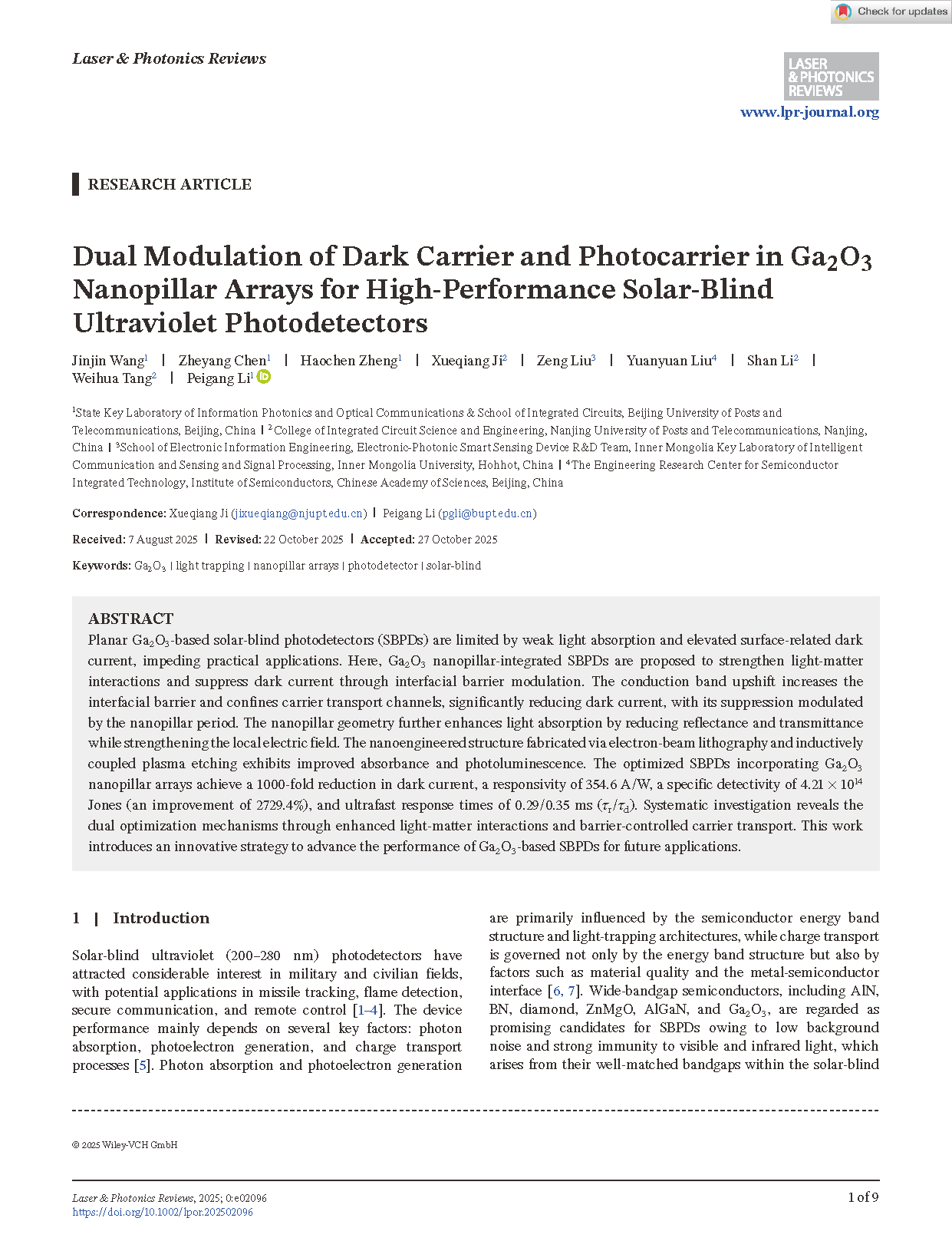
Figure 1 illustrates the simulated current-density distribution and electric-field enhancement in the Ga₂O₃ nanopillar arrays, revealing both the carrier-transport limitations and the characteristics of localized optical fields.
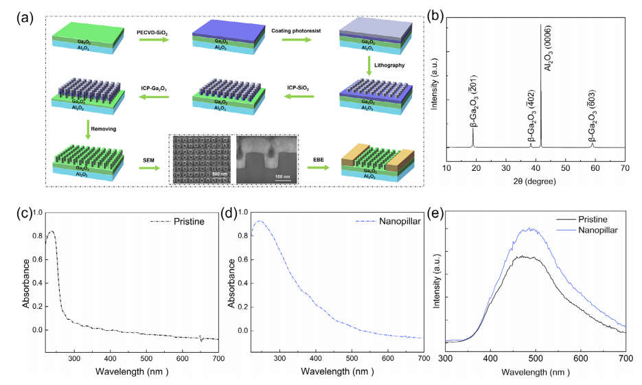
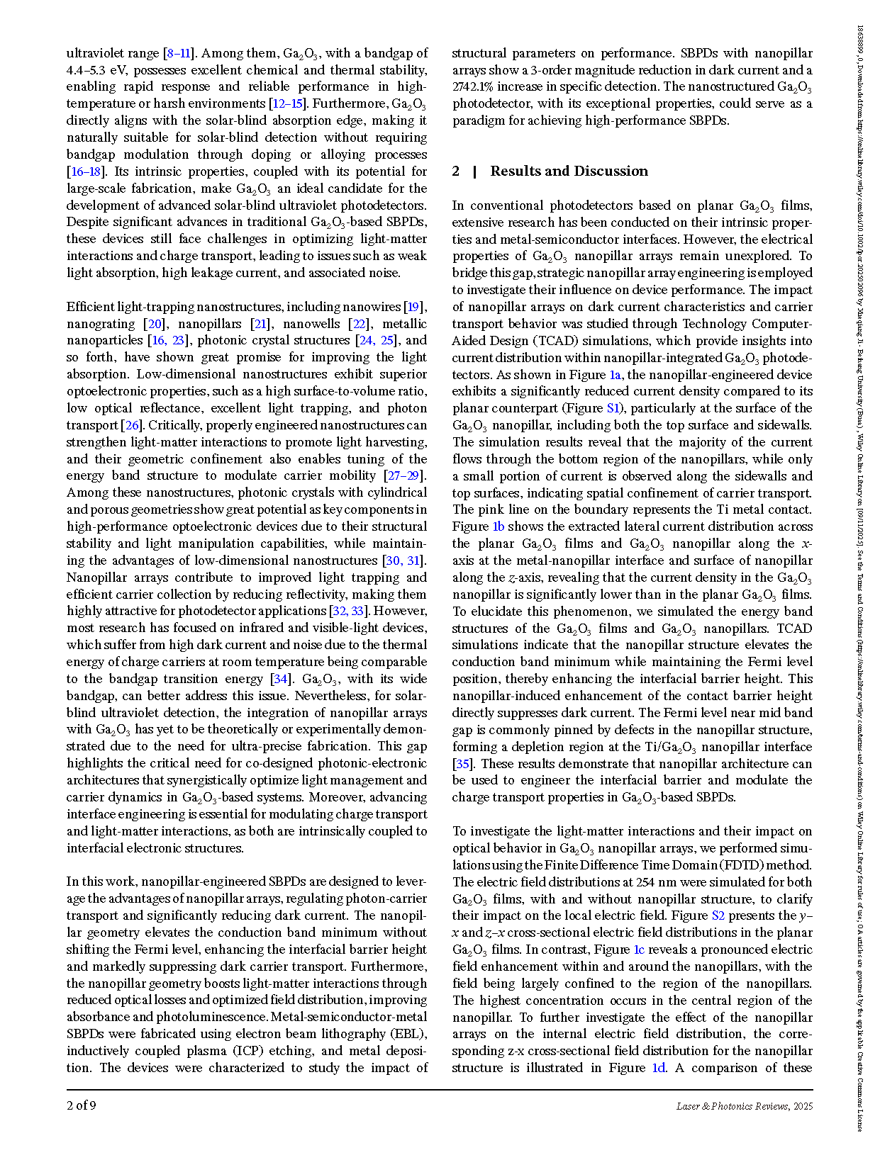
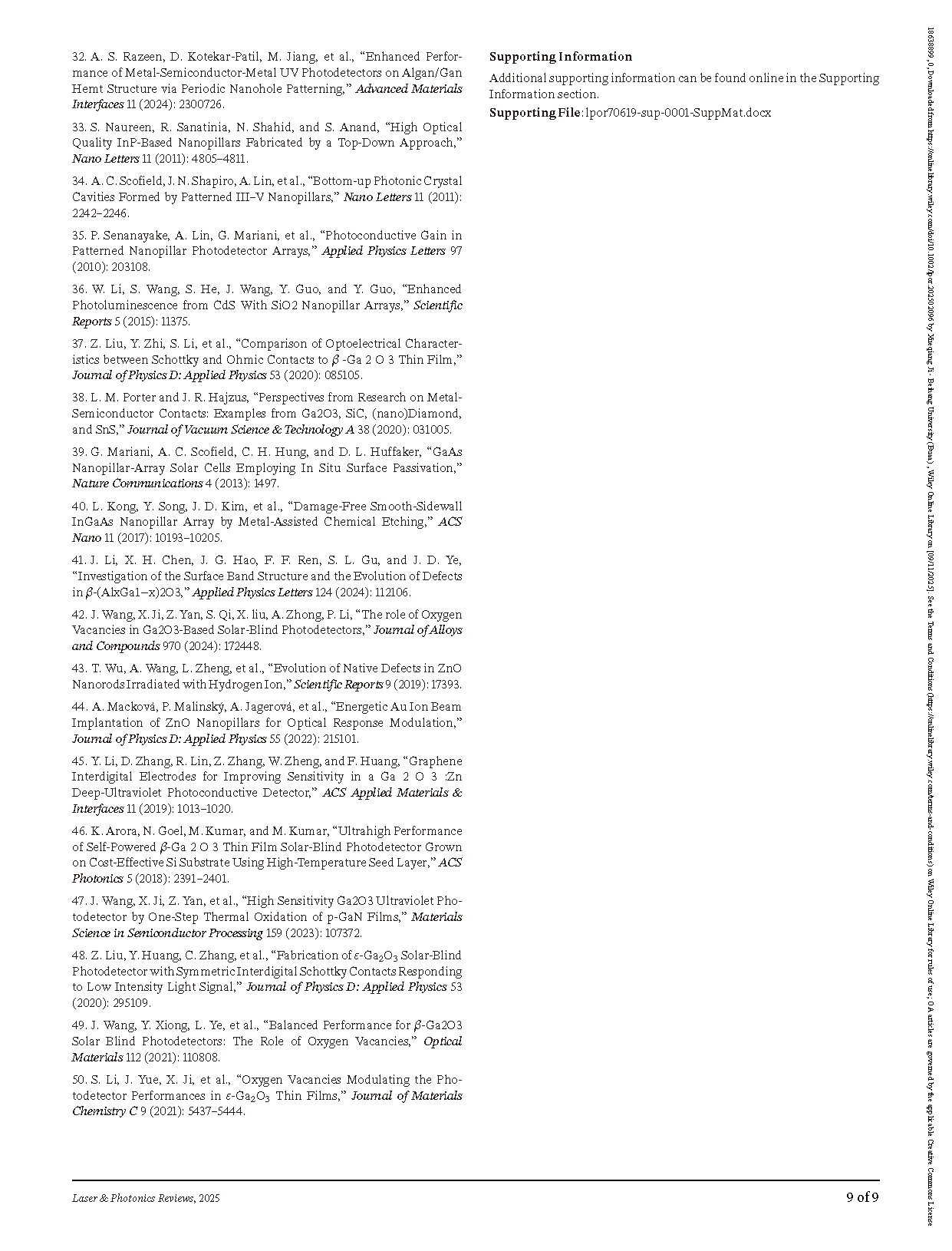
Figure 2 presents the fabrication process and material characterization of the nanopillar arrays, including XRD patterns and UV–Vis absorption spectra, confirming that the nanostructure enhances optical absorption and photoluminescence intensity.

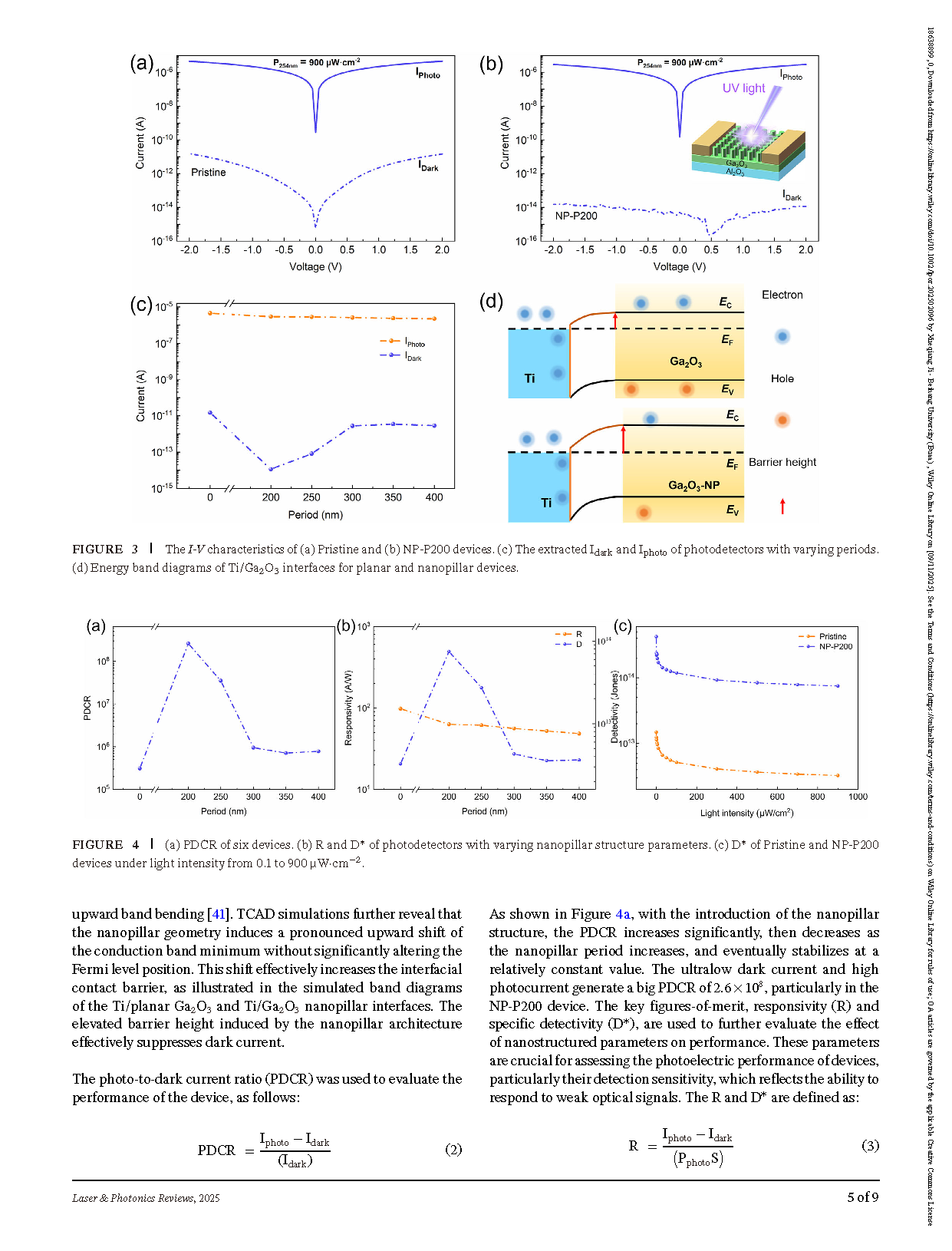
Figure 3 analyzes the I–V characteristics and band diagrams, showing that the nanopillar structure significantly suppresses dark current and increases the interfacial barrier height.
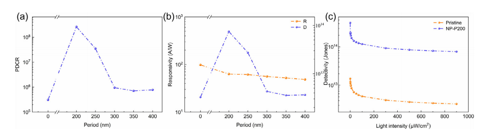
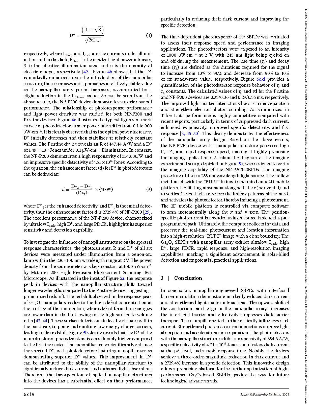
Figure 4 compares the PDCR, responsivity, and specific detectivity of devices with different nanopillar periods, highlighting the NP-P200 device as the optimal design.
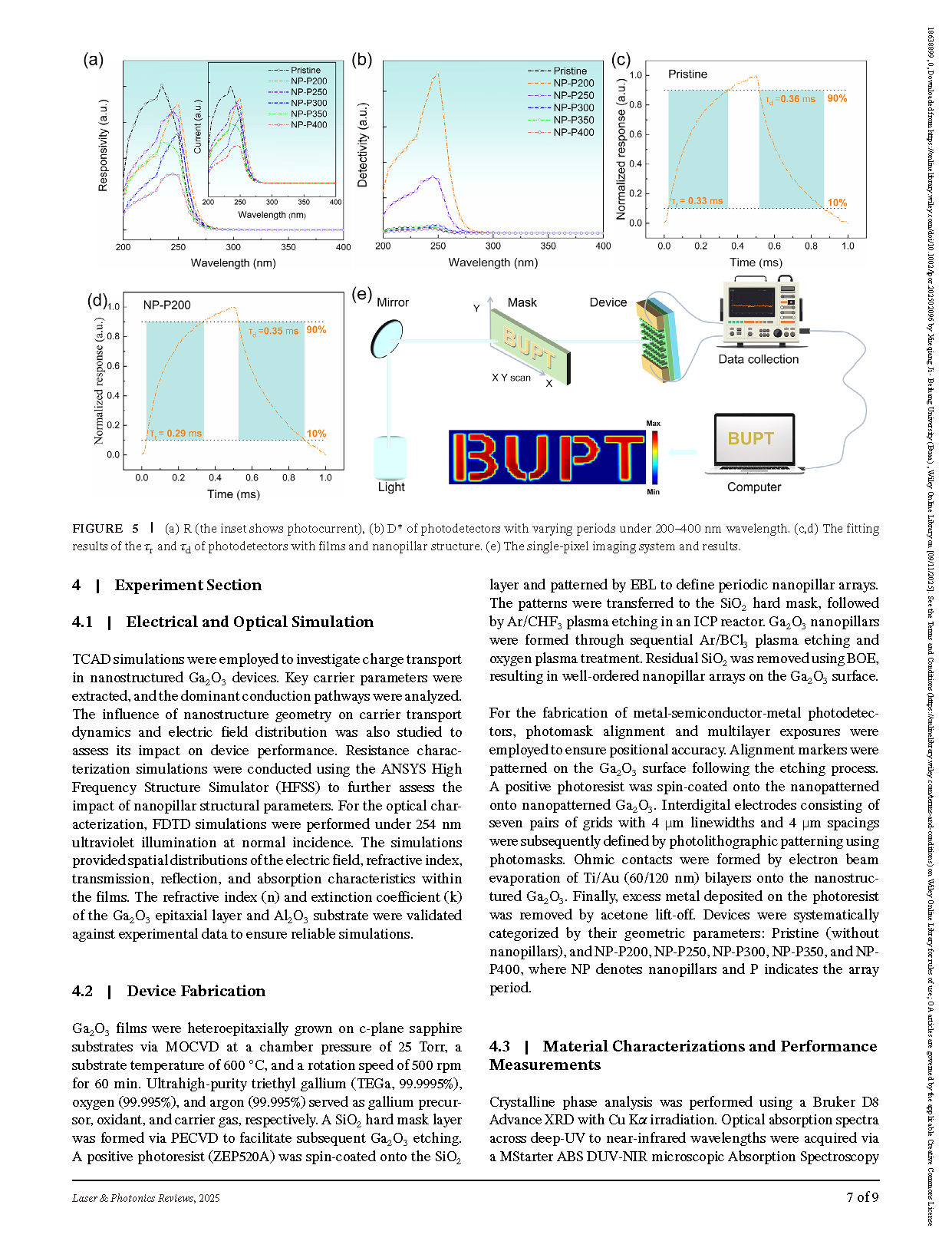
Figure 5 displays the spectral response, temporal characteristics, and a single-pixel imaging demonstration, verifying the device’s fast response and imaging capability.
Insights
This study achieves a major performance leap in Ga₂O₃ solar-blind ultraviolet photodetectors through nanopillar-array engineering, reducing the dark current to the pA level, boosting detectivity by 2729.4%, and achieving a fast response time of 0.29 ms. The key innovation lies in the synergistic optimization of photonic and electronic design via nanostructure engineering, offering a scalable fabrication paradigm for wide-bandgap semiconductor photodetectors. The findings suggest that strategies for modulating interfacial barriers and optical-field distributions using nanostructures can be broadly applied to other optoelectronic systems, enabling high-performance devices for harsh-environment applications.
DOI:
https://doi.org/10.1002/lpor.202502096