Paper Sharing
【International Papers】Defect Analysis of the β– to γ–Ga₂O₃ Phase Transition
日期:2025-12-04阅读:455
Researchers from the GFZ Helmholtz Centre for Geosciences have published a dissertation titled "Defect Analysis of the β– to γ–Ga2O3 Phase Transition" in Advanced Functional Materials.
Background
Throughout the history of science and engineering, there has always been a drive to find new and superior materials to advance technology. This is also true for power electronics, which needs new materials and related research activities to ensure future developments. Gallium oxide (Ga2O3) is a promising candidate for future ultrawide-bandgap (UWB) semiconductor materials for power electronic devices. It has two main advantages over the traditional UWB semiconductor materials, such as silicon carbide and gallium nitride. Ga2O3 does not only have a superior breakdown voltage, which allows to increase the device performance, but cost-effective large wafer production by melt growth methods is also possible with Ga2O3. Furthermore, the existence of different polymorphs of Ga2O3 makes it a compelling material for crystal structure engineering. This might be achieved via fabrication of different polymorphic layers on a single wafer as well as engineering of nanostructures with different polymorphs. However, most research has focused on the β phase, which is the most chemically and thermally stable polymorph of Ga2O3.
Abstract
This study investigates the ion irradiation induced phase transition in gallium oxide (Ga2O3) from the β to the γ phase, the role of defects during the transformation, and the quality of the resulting crystal structure. Using a multi-method analysis approach including X-ray diffraction (XRD), transmission electron microscopy (TEM), Rutherford backscattering spectrometry in channeling mode (RBS/c), Doppler broadening variable energy positron annihilation spectroscopy (DB-VEPAS), and variable energy positron annihilation lifetime spectroscopy (VEPALS) supported by density functional theory (DFT) calculations, defects at all the relevant stages of the phase transition are characterized. A reduction in backscattering yield is observed in RBS/c spectra after the transition to the γ phase. This goes hand in hand with a significant decrease in the positron trapping center density due to generation of embedded vacancies intrinsic for the γ–Ga2O3 but too shallow in order to trap positrons. A comparison of the observed positron lifetime of γ–Ga2O3 with different theoretical models shows good agreement with the three-site γ phase approach. A characteristic increase in the effective positron diffusion length and the positron lifetime at the transition point from β–Ga2O3 to γ–Ga2O3 enables visualization of the phase transition with positrons for the first time. Moreover, a subsequent reduction of these quantities with increasing irradiation fluence is observed, which attributes to further evolution of the γ–Ga2O3 and changes in the gallium vacancy density as well as relative occupation in the crystal lattice.
Conclusion
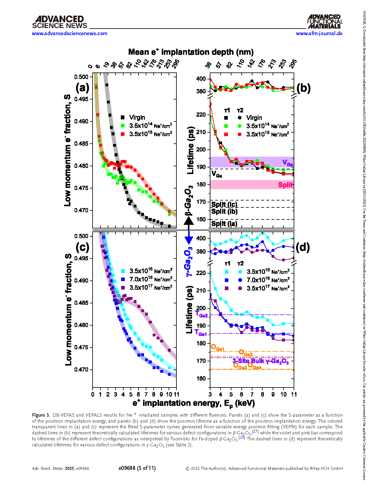
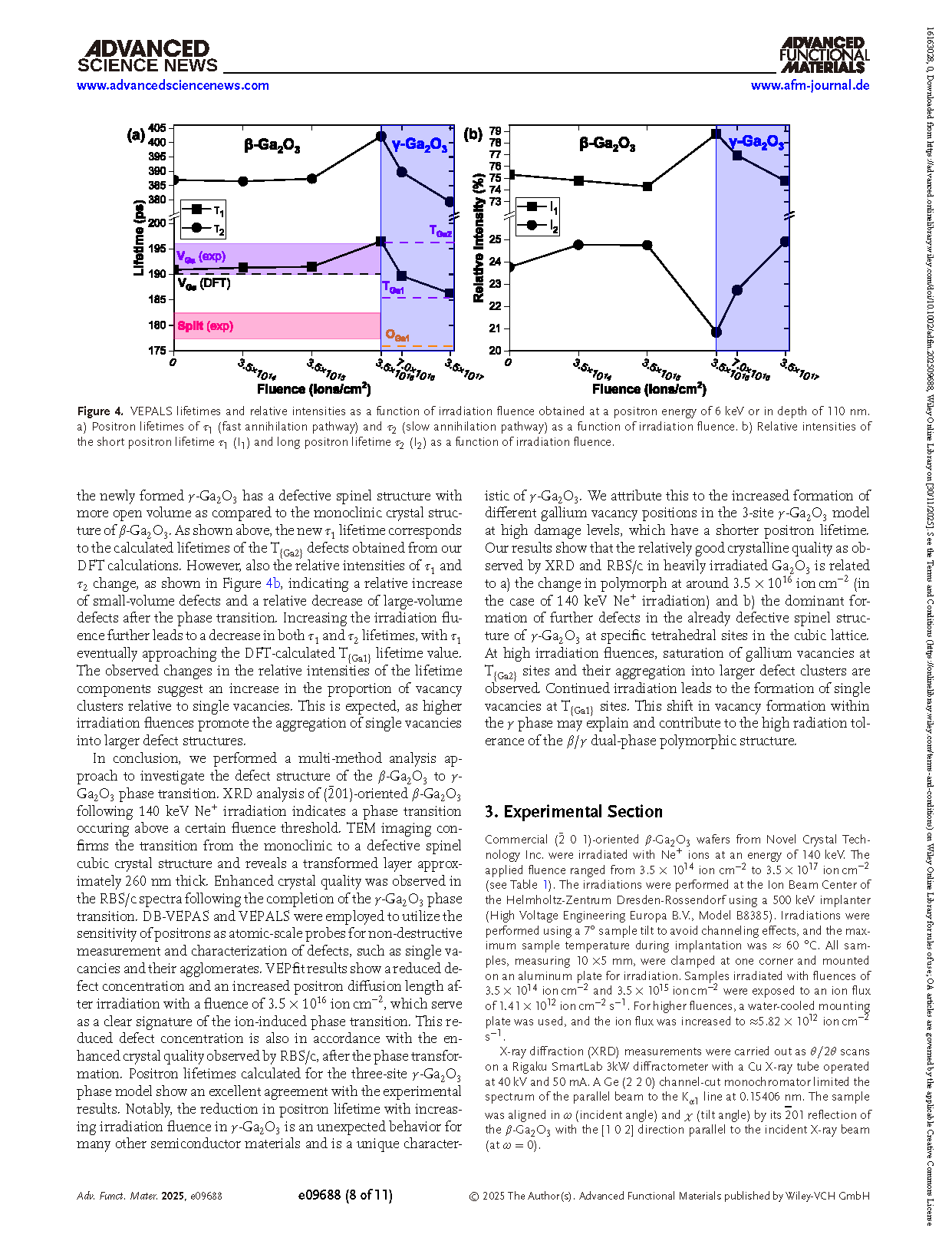
In conclusion, we performed a multi-method analysis approach to investigate the defect structure of the β-Ga2O3 to γ-Ga2O3 phase transition. XRD analysis of (-201)-oriented β-Ga2O3 following 140 keV Ne+ irradiation indicates a phase transition occuring above a certain fluence threshold. TEM imaging confirms the transition from the monoclinic to a defective spinel cubic crystal structure and reveals a transformed layer approximately 260 nm thick. Enhanced crystal quality was observed in the RBS/c spectra following the completion of the γ-Ga2O3 phase transition. DB-VEPAS and VEPALS were employed to utilize the sensitivity of positrons as atomic-scale probes for non-destructive measurement and characterization of defects, such as single vacancies and their agglomerates. VEPfit results show a reduced defect concentration and an increased positron diffusion length after irradiation with a fluence of 3.5 × 10¹⁶ ion cm−2, which serve as a clear signature of the ion-induced phase transition. This reduced defect concentration is also in accordance with the enhanced crystal quality observed by RBS/c, after the phase transformation. Positron lifetimes calculated for the three-site γ-Ga2O3 phase model show an excellent agreement with the experimental results. Notably, the reduction in positron lifetime with increasing irradiation fluence in γ-Ga2O3 is an unexpected behavior for many other semiconductor materials and is a unique characteristic of γ-Ga2O3. We attribute this to the increased formation of different gallium vacancy positions in the 3-site γ-Ga2O3 model at high damage levels, which have a shorter positron lifetime. Our results show that the relatively good crystalline quality as observed by XRD and RBS/c in heavily irradiated Ga2O3 is related to a) the change in polymorph at around 3.5 × 10¹⁶ ion cm−2 (in the case of 140 keV Ne+ irradiation) and b) the dominant formation of further defects in the already defective spinel structure of γ-Ga2O3 at specific tetrahedral sites in the cubic lattice. At high irradiation fluences, saturation of gallium vacancies at T{Ga2} sites and their aggregation into larger defect clusters are observed. Continued irradiation leads to the formation of single vacancies at T{Ga1} sites. This shift in vacancy formation within the γ phase may explain and contribute to the high radiation tolerance of the β/γ dual-phase polymorphic structure.
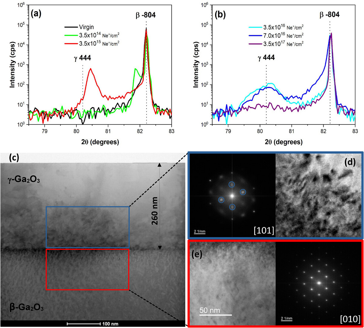
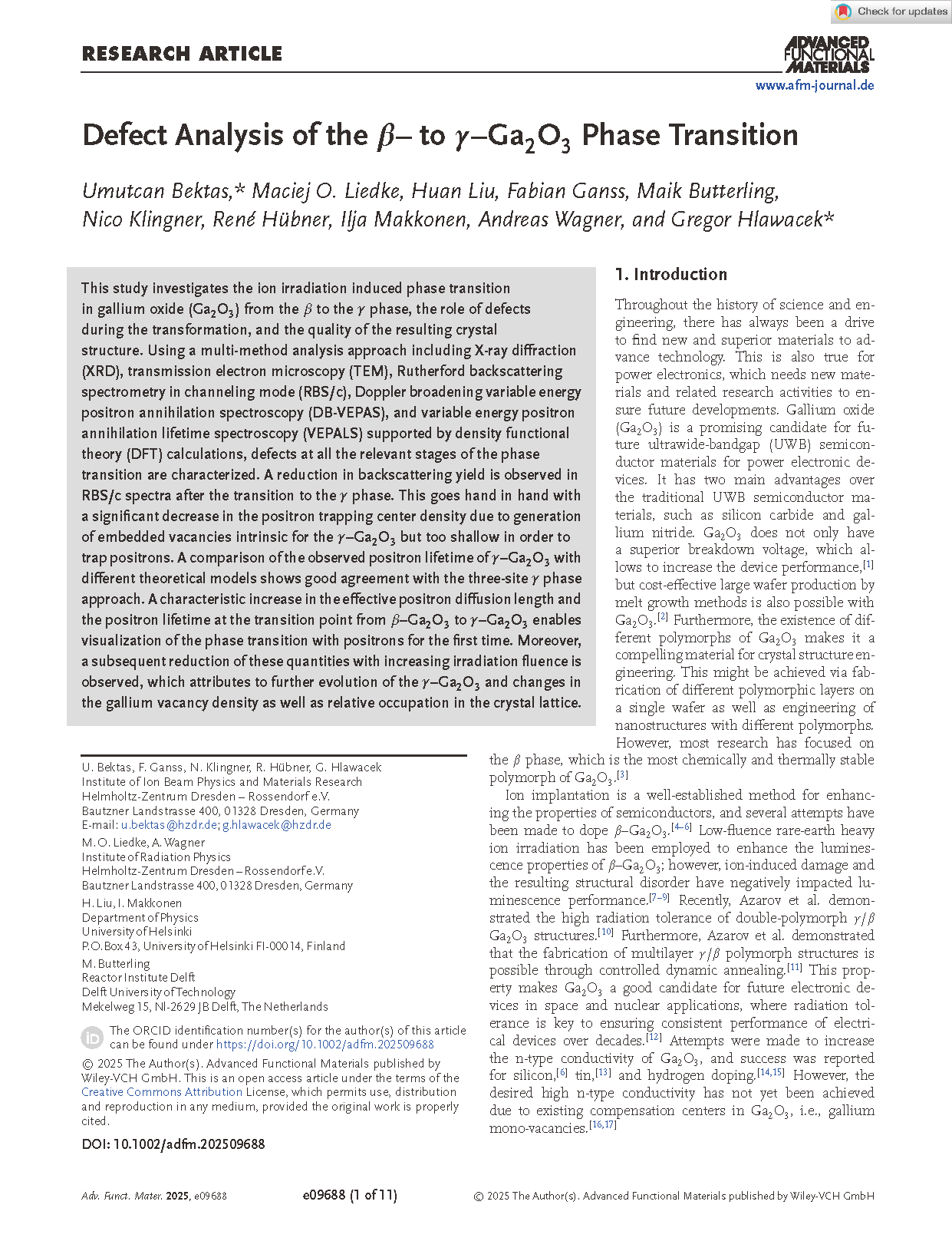
Figure 1. Structure analysis of β–Ga2O3 irradiated with different fluences of 140 keV Ne+. a) XRD patterns of the virgin and irradiated samples with low fluences, b) XRD patterns of the irradiated samples with high fluences. c) bright-field scanning transmission electron microscopy (BF-STEM) image of the converted layer on top of pristine β–Ga2O3. d) high-resolution transmission electron microscopy (HRTEM) image (right) and fast Fourier transform (FFT) (left) of theγ layer close to the interface along [1 0 1] zone axis. The diffraction spots highlighted by the blue circles correspond to the γ–Ga2O3 {111} reflections. e) HRTEM image and FFT pattern of the β region close to the interface along [0 1 0] zone axis.
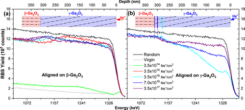
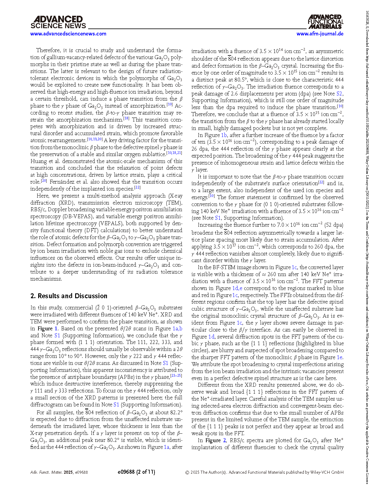
Figure 2. RBS/c spectra for β-Ga2O3 irradiated with different fluences. The irradiated area is converted from β-Ga2O3 to γ-Ga2O3 for 3.5 × 10¹⁶ ion cm−2 and higher fluences. a) RBS/c spectra obtained after aligning to the [-2 0 1] β-Ga2O3 channeling direction. b) RBS/c spectra obtained after the phase transformation and realignment to the [111] γ-Ga2O3 channeling direction. The dashed lines in the sample configuration inset are only a sketch of the lattice planes and do not represent the actual misalignment. Of note, the depth scale is calculated for gallium atoms.
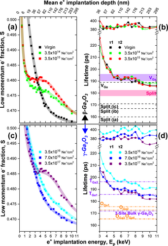
Figure 3. DB-VEPAS and VEPALS results for Ne+-irradiated samples with different fluences. Panels (a) and (c) show the S-parameter as a function of the positron implantation energy, and panels (b) and (d) show the positron lifetime as a function of the positron implantation energy. The colored transparent lines in (a) and (c) represent the fitted S-parameter curves generated from variable energy positron fitting (VEPfit) for each sample. The dashed lines in (b) represent theoretically calculated lifetimes for various defect configurations in β-Ga2O3, while the violet and pink bar correspond to lifetimes of the different defect configurations as interpreted by Tuomisto for Fe-doped β-Ga2O3. The dashed lines in (d) represent theoretically calculated lifetimes for various defect configurations in γ-Ga2O3.
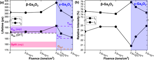
Figure 4. VEPALS lifetimes and relative intensities as a function of irradiation fluence obtained at a positron energy of 6 keV or in depth of 110 nm. a) Positron lifetimes of τ1 (fast annihilation pathway) and τ2 (slow annihilation pathway) as a function of irradiation fluence. b) Relative intensities of the short positron lifetime τ1 (I1) and long positron lifetime τ2 (I2) as a function of irradiation fluence.
DOI:
doi.org/10.1002/adfm.202509688