


Member News
【Member News】Garen Semiconductor’s Breakthrough in 8-Inch Gallium Oxide Selected as a 2025 Major Scientific and Technological Achievement of Zhejiang Province
日期:2025-12-04阅读:661
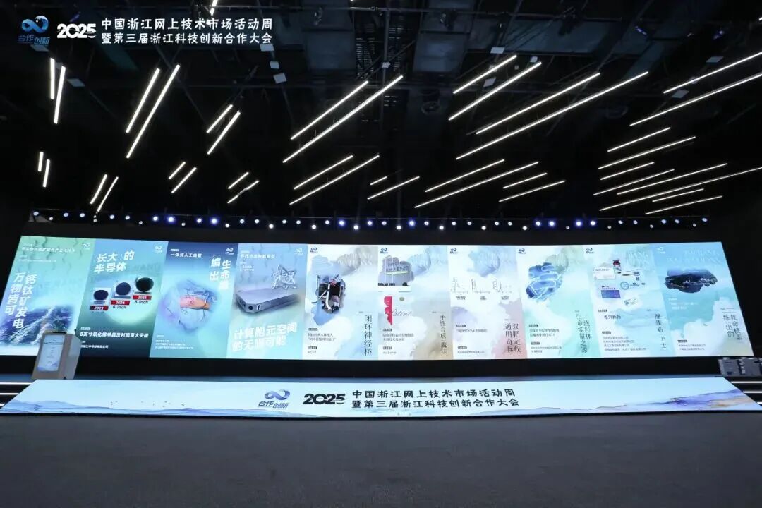
In November 2025, the 2025 China Zhejiang Online Technology Market Week & the 3rd Zhejiang Science and Technology Innovation Cooperation Conference was grandly held in Hangzhou. Hangzhou Garen Semiconductor Co., Ltd. (“Garen Semiconductor”) was successfully selected by the Zhejiang Provincial Department of Science and Technology for its “Major Breakthrough in 8-Inch Gallium Oxide Single Crystals and Substrates,” becoming an important representative of Zhejiang’s “hard-core” scientific and technological strength. This achievement marks a critical leap for China’s ultra-wide-bandgap semiconductor field—from “following” to “leading.”
Breaking International Monopoly:
8-Inch Gallium Oxide Achievement Accelerates Industrial Deployment
As a core material of the fourth-generation semiconductors, Gallium Oxide is regarded as a key enabler for high-voltage new-energy vehicle platforms, smart grids, and power systems in AI data centers, thanks to its ultra-wide bandgap and exceptional breakdown field strength. However, for years, global Gallium Oxide substrate manufacturing has been constrained by traditional crystal growth technologies, leading to major limitations including small wafer sizes, high production costs, and incompatibility with mainstream silicon-based production lines. These bottlenecks have significantly restricted the pace of industrialization.
Leveraging the scientific strength of the National Key Laboratory of Silicon and Advanced Semiconductor Materials at Zhejiang University and the Zhejiang University Hangzhou Global Scientific and Technological Innovation Center, GAREN Semiconductor has built a world-class R&D team under the guidance of Prof. Yang Deren, Academician of the Chinese Academy of Sciences, who serves as the chief scientific advisor. The company pioneered a proprietary “Casting Method” for Gallium Oxide single-crystal growth—successfully overcoming multiple long-standing industry challenges.
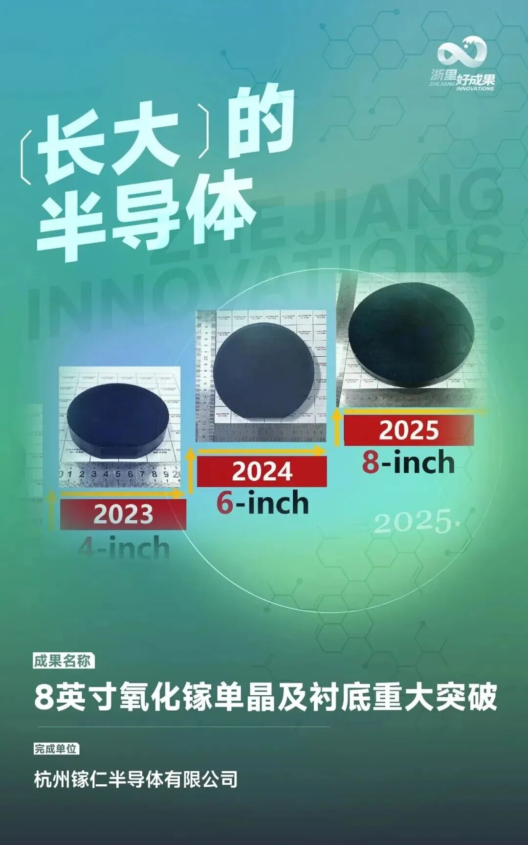
Within just three years, GAREN Semiconductor achieved a leapfrog advancement from 2-inch to 8-inch Gallium Oxide substrates, setting a remarkable industry record of “one wafer size breakthrough per year.”
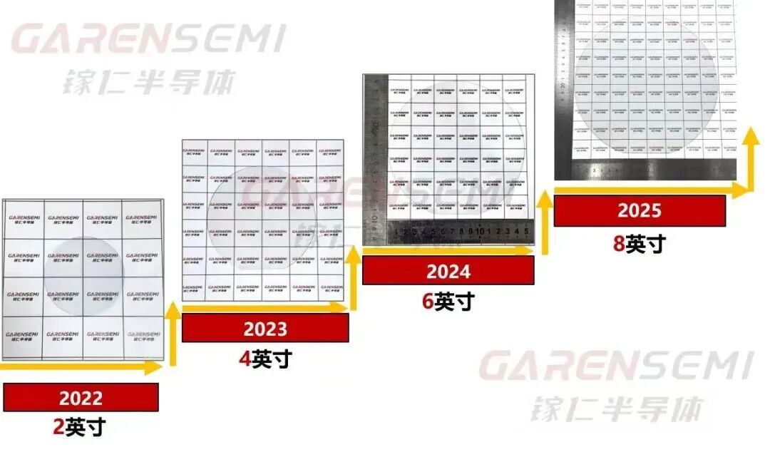
Size of GAREN SEMI Gallium Oxide substrate rapid evolution
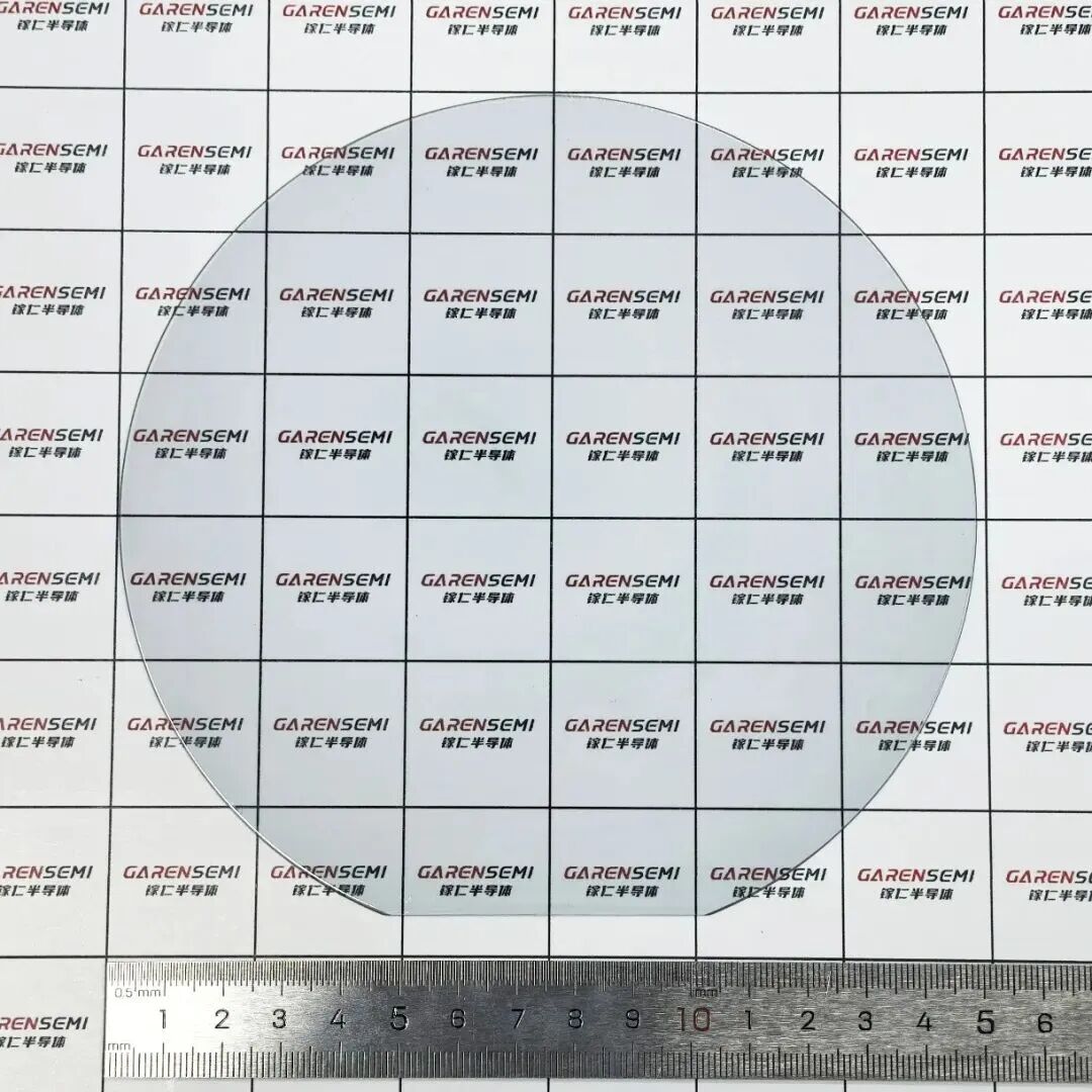
In March 2025, the company globally debuted its 8-inch Gallium Oxide single crystal and substrate, becoming the first enterprise worldwide to master the growth technology for this dimension. In July of the same year, GAREN SEMI’s 8-inch products passed certification by authoritative institutions at home and abroad, including the Shenzhen Pinghu Laboratory and the Malvern Panalytical Asia-Pacific Application Center. The XRD rocking curve exhibited a minimum full width at half maximum (FWHM) of only 12.4 arcsec, with all values below 30 arcsec, reaching an internationally leading level.
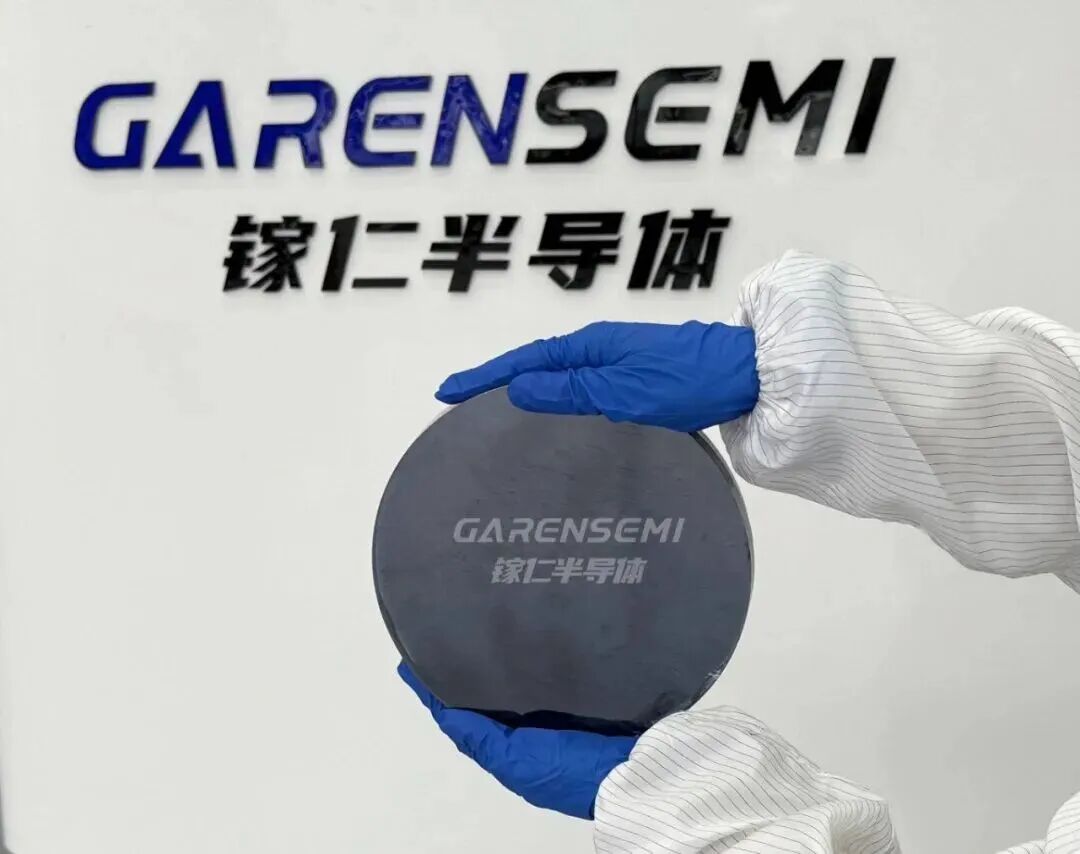
GAREN SEMI’s 8-inch Gallium Oxide Breakthrough
Not only does this achievement set a new global record for Gallium Oxide substrate size, but it also holds strong potential for full compatibility with existing silicon-based production lines. By significantly improving material utilization and dramatically lowering overall manufacturing costs, this milestone lays a crucial foundation for enabling Gallium Oxide to move from the laboratory into mass-production fabs.
Multiple Honors Highlight the Innovation Strength of Zhejiang’s Semiconductor Enterprises
2025 marked a year of significant breakthroughs for Garen Semiconductor. In addition to being selected as one of the Major Scientific and Technological Achievements of 2025 by the Zhejiang Provincial Department of Science and Technology, the company has also earned several prestigious industry awards for its technological innovation and contributions to industrialization—solidifying its position as a “benchmark force” in the regional semiconductor sector.
2025.03
GAREN SEMI was awarded the "SEMI Outstanding Contribution Award for Sustainable Development" at SEMICON CHINA, the world's largest semiconductor industry event, highlighting the concept of green production.
2025.04
GAREN SEMI won the " Solidarity Colleagues Award" at the 2025 Jiufengshan Conforence (JFSC), demonstrating the value of industrial chain collaboration.
2025.05
GAREN SEMI was awarded the "Innovation Vitality Award" in the semiconductor industry of Zhejiang Province for its technological innovation capabilities, becoming a benchmark in the local semiconductor industry.
2025.09
GAREN SEMI represented the Hangzhou region and won the second prize in the enterprise group of the 10th "Maker China" Zhejiang Provincial Finals, demonstrating its outstanding technological innovation capabilities and industrialization achievements.
2025.10
GAREN SEMI achieved a double celebration - not only did it successfully enter the top 500 of the national enterprise group in the 10th "Maker China" Small and Medium-sized Enterprises Innovation and Entrepreneurship Competition, but it also shared the "2024-2025 Semiconductor Materials Industry Contribution Award" with four leading enterprises in the domestic semiconductor materials field.
2025.11
At The 11th International Forum on Wide Bandgap Semiconductors & the 22nd China International Forum on Solid State Lighting (IFWS & SSLCHINA 2025), Garen Semiconductor was selected for the “Top 10 China Third-Generation Semiconductor Technology Advances of 2025” with its achievement “Major Breakthrough in 8-inch Ga₂O₃ Single Crystal and Substrate Preparation.” This recognition highlights the innovative strength and industry leadership of semiconductor enterprises in Zhejiang Province.
Rooted in Zhejiang, Expanding Nationwide:
Building Global Competitiveness Through Industrial Leadership
Since its establishment in September 2022 in Xiaoshan District, Hangzhou, Garen Semiconductor has remained firmly rooted in Zhejiang’s fertile ground for innovation, leveraging local policies and industrial ecosystem advantages to achieve rapid growth. After settling in Xiaoshan, the company successively received recognition under the “5213” talent program and the Leading Innovation & Entrepreneurship Project, and secured nearly 100 million RMB in Pre-A round financing in 2024, injecting strong momentum into technological R&D and industrialization.
At present, the company has been certified as a National Technology-Based SME and a Zhejiang Province “Specialized, Refined, Differential, and Innovative (SRDI)” SME, forming a positive development pattern driven by policy empowerment, capital support, and technological innovation.
In terms of market deployment, Garen Semiconductor has achieved full-scale implementation from core equipment to key materials.
On the equipment side, the company has independently developed crystal growth equipment for Gallium Oxide dedicated to VB-method. The system uses a non-iridium (Ir-free) crucible and operates under ambient air atmosphere, enabling stable growth of large-size single crystals with multiple orientations while supporting further scale-up. It has already been supplied in batches to more than ten domestic universities, research institutes, and semiconductor companies, accelerating downstream development of large-diameter Ga₂O₃ materials.
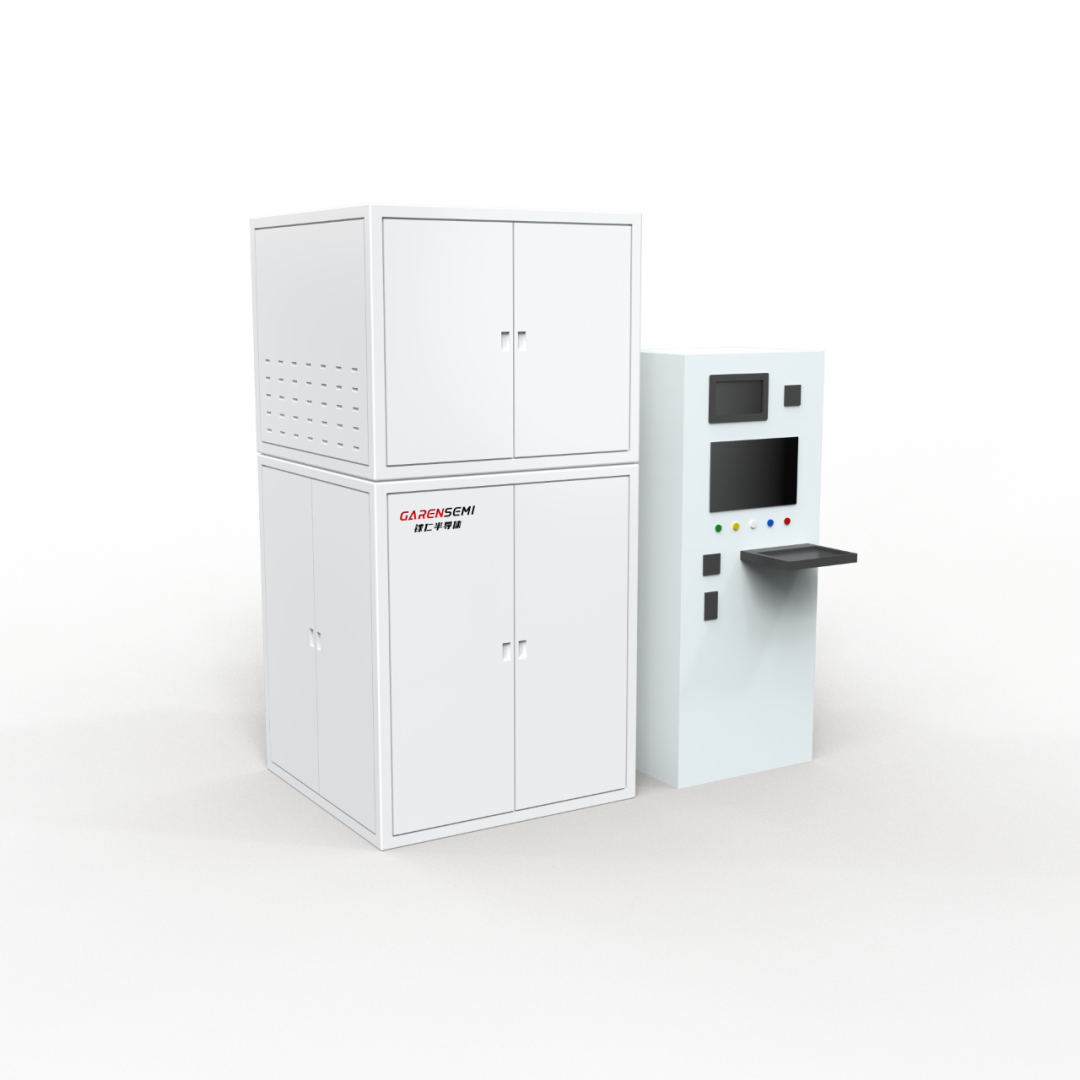
Garen Semiconductor’s self-developed VB-method crystal growth equipment
On the materials side, beyond large-size Ga₂O₃ substrates, the company has achieved stable mass production of (011)-oriented gallium oxide wafers. Leveraging the unique characteristics of this crystal orientation, these substrates meet diversified application needs such as high-frequency devices and sensors, and have already completed supply verification with multiple customers.
Meanwhile, the thick-film homoepitaxial Ga₂O₃ wafers (thickness >10 μm), featuring outstanding thickness uniformity (σ < 1%) and high crystalline quality (XRD rocking curve FWHM < 40 arcsec), have become a core choice for high-performance power-device manufacturers.
6-inch Ga₂O₃ Homoepitaxial Wafer by Garen Semiconductor
In terms of industry standards development and technology transfer, Garen Semiconductor is also actively contributing its “Garen Intelligence.” In 2025, the company not only served as the lead drafting organization in the review of two group standards — “Dislocation Density Measurement Method for Gallium Oxide Single Crystals” and “β-Gallium Oxide Homoepitaxial Wafers” — but also participated in the proposal of the group standard “Semi-Insulating Silicon Carbide Wafers for Augmented Reality (AR) Glasses”. These efforts have helped lay the groundwork for the standardized and normative development of the Gallium Oxide industry in Zhejiang Province and across China.
In addition, the national standard “Test Method for Transmittance of Semiconductor Single Crystal Materials,” co-drafted by Garen Semiconductor, has been officially released. This standard fills a domestic gap in the field of transmittance measurement for semiconductor single crystals and provides a unified and authoritative testing reference for the industry.
Looking ahead, Garen Semiconductor will continue to take Zhejiang as its core innovation hub, advancing the size scaling and quality enhancement of Gallium Oxide materials while accelerating the industrialization of its casting-growth technology. The company will further deepen its national market presence, strengthen international technical cooperation, and strive for new breakthroughs in larger-size and higher-performance Gallium Oxide materials. With these efforts, Garen Semiconductor aims to support the establishment of Zhejiang as a global innovation center for ultrawide-bandgap semiconductors and contribute “Garen Strength” to China’s independent and secure semiconductor development.
For more information about GAREN SEMI and its products
Visit our official website: http://garen.cc/
Or contact us in the following ways:
Mr. Jiang :15918719807
Email :jiangjiwei@garen.cc
Mr. Xia :19011278792
Email :xianing@garen.cc
