Paper Sharing
【Member Papers】Single-event burnout mechanism in β-Ga₂O₃ Schottky barrier diodes
日期:2025-11-30阅读:475
Researchers from the Xidian University have published a dissertation titled "Single-event burnout mechanism in β-Ga2O3 Schottky barrier diodes" in Applied Physics Letters.
Project Support
This research was supported in part by the National Science Fund for Distinguished Young Scholars under Grant No. 62525402, in part by the National Natural Science Foundation of China under Grant No. 62404164, and in part by the National Key Research and Development Program of China under Grant Nos. 2022YFB3604203 and 2021YFB3601102.
Background
β-Ga₂O₃, with its ultra-wide bandgap, high breakdown field, and strong intrinsic radiation resistance, is a promising semiconductor material for high-power device applications. Schottky barrier diodes (SBDs) based on β-Ga₂O₃ are particularly attractive for aerospace applications but remain susceptible to single-event effects (SEE) induced by high-energy heavy ions, such as single-event burnout (SEB). Previous studies on materials like SiC and GaN have shown that SEB is mainly caused by local overheating and defect-induced conductive paths. However, the radiation-sensitive regions and the detailed breakdown mechanisms in β-Ga₂O₃ SBDs have not yet been fully elucidated. Therefore, investigating the SEB characteristics of β-Ga₂O₃ SBDs, identifying radiation-sensitive regions, and revealing the underlying failure mechanisms are crucial for guiding future radiation-hardening optimization of β-Ga₂O₃ devices.
Abstract
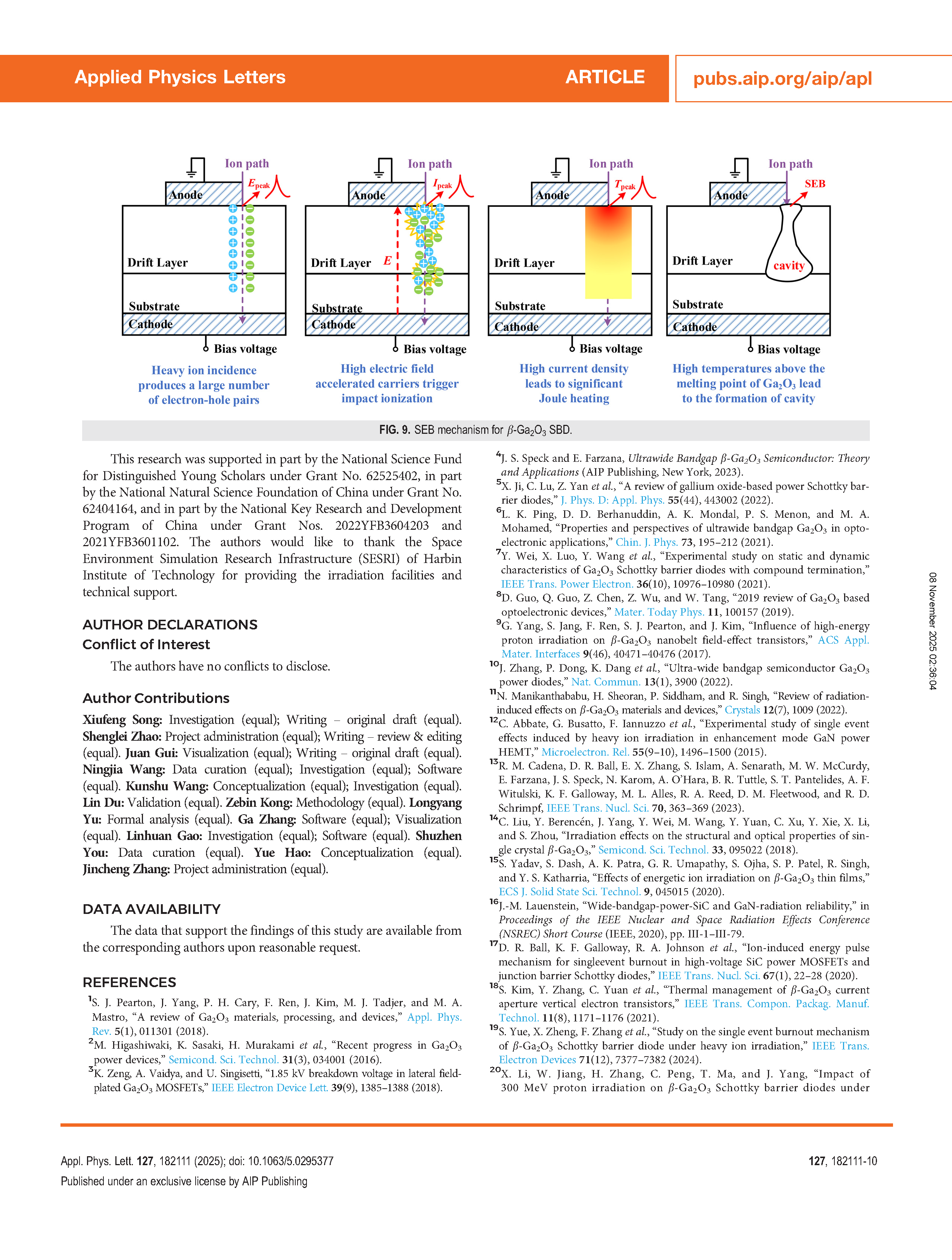
In this work, the single-event burnout (SEB) mechanism of β-Ga2O3 SBD is systematically investigated. The irradiation experiment was performed based on Kr ions with a high linear energy transfer of 37.9 MeV/(mg/cm2). During irradiation, the SBDs experienced burnout at applied bias voltages of 300 and 500 V, and the failure points were found at the anode edge. The TCAD simulation results show that the region outside the anode is less sensitive to irradiation. In contrast, ion incidence in the anode region leads to significant increases in electric field, current density, and temperature. Furthermore, there is a significant increase in these parameters at the anode edge compared to the anode center. Therefore, the anode edge is identified as the most sensitive region to radiation, which is consistent with the experimental results. Based on experimental and simulation results, an SEB mechanism is proposed. Heavy ion incidence will introduce a large number of electron–hole pairs, which are subsequently accelerated by the peak electric field at the anode edge. This acceleration initiates impact ionization, leading to the continuous generation of additional electron–hole pairs and resulting in a peak current at the anode edge. The current induced by the irradiation will cause significant Joule heating. When the local lattice temperature exceeds the melting temperature of β-Ga2O3 material, it gradually leads to thermal damage and triggers SEB. This paper analyzed the radiation-sensitive regions and the mechanism of SEB in β-Ga2O3 SBD, which provides a research basis for future heavy-ion irradiation hardening.
Conclusion
This study systematically elucidates the single-event burnout (SEB) mechanism in β-Ga₂O₃ Schottky barrier diodes under high-energy ion irradiation. The results reveal that device failure primarily originates from electric field crowding at the anode edge. When energetic ions penetrate the β-Ga₂O₃ layer, dense electron–hole pairs are generated, leading to local avalanche multiplication that further enhances current density and electric field strength. The resulting transient power dissipation causes rapid temperature rise, and due to the inherently low thermal conductivity of β-Ga₂O₃, localized heat cannot dissipate efficiently, triggering thermal runaway and irreversible burnout. Both simulation and experimental results consistently confirm that the coupling of electric field concentration and thermal accumulation is the fundamental cause of SEB. Furthermore, incorporating a field plate and optimizing the anode edge geometry effectively homogenize the electric field distribution and reduce peak temperature, thereby significantly improving the device’s SEB robustness. This work provides essential insights into the failure physics of β-Ga₂O₃ power devices and offers practical design guidance for enhancing their radiation tolerance and reliability.
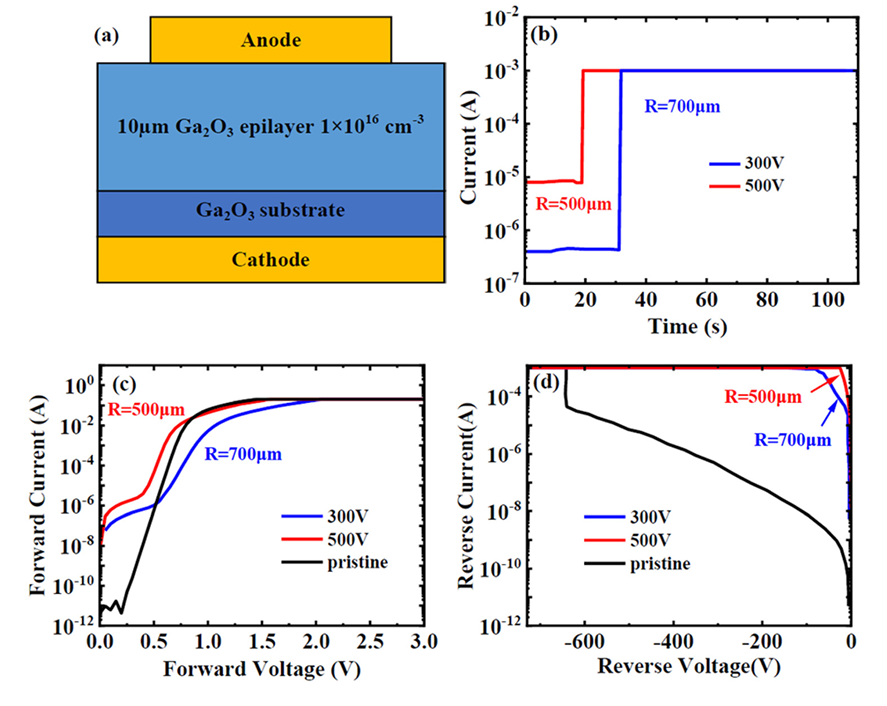
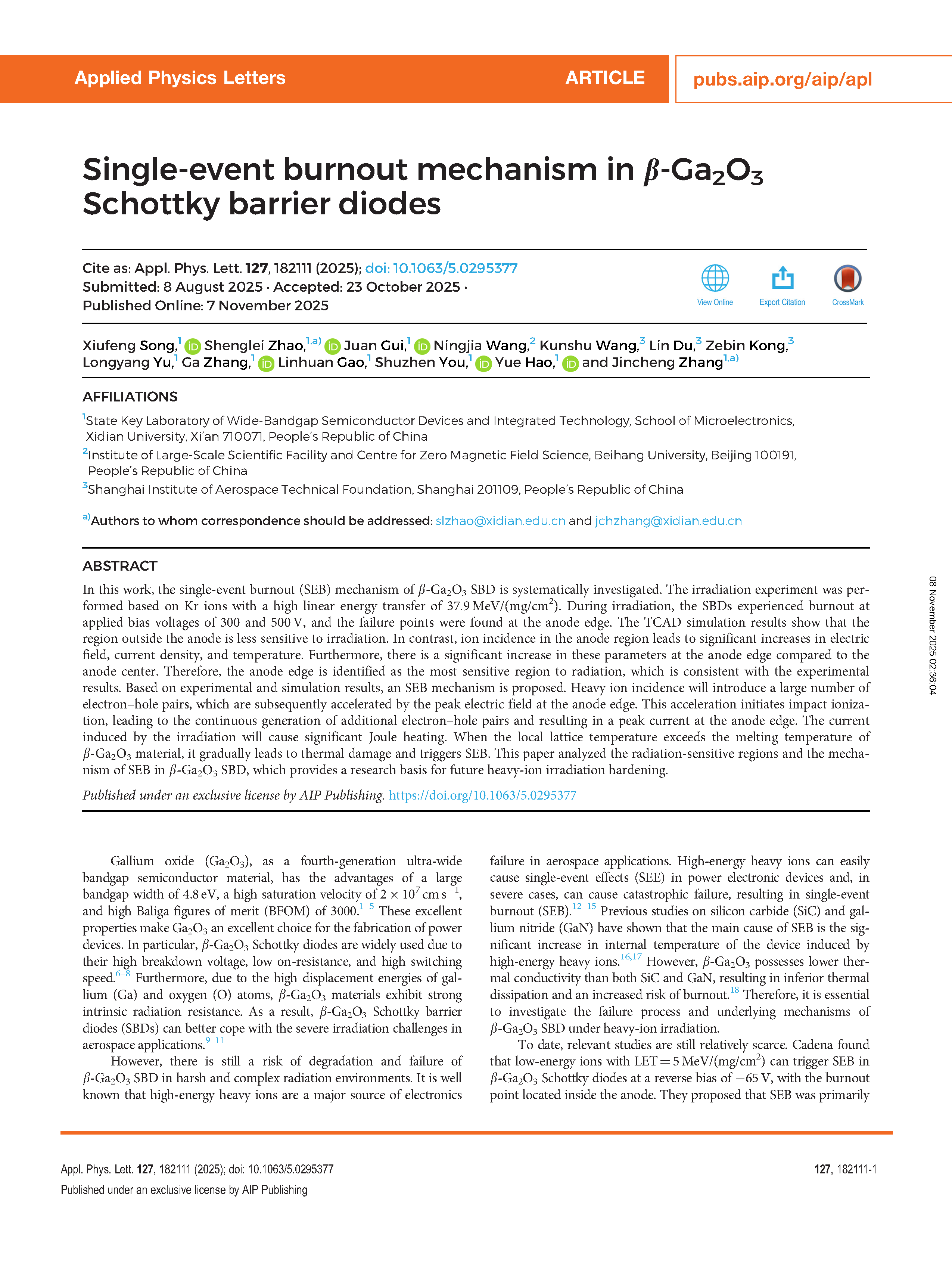
Fig. 1. (a) Structural diagram of the β-Ga₂O₃ SBD; (b) real-time current monitoring of β-Ga₂O₃ SBDs under irradiation; (c) forward I–V characteristics of pristine and burnout β-Ga₂O₃ SBDs at bias voltages of 300 and 500 V; (d) reverse I–V characteristics of pristine and burnout β-Ga₂O₃ SBDs at bias voltages of 300 and 500 V. (Red and blue curves represent devices with anode radius R of 500 μm and 700 μm, respectively.)
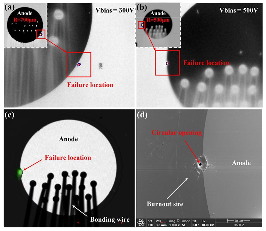
Fig. 2. Thermal failure analysis results of SEB β-Ga₂O₃ SBDs at bias voltages of (a) 300 V and (b) 500 V, with anode radii (R) of 700 μm and 500 μm, respectively. (The glowing spots indicate the burnout points.) (c) OBIRCH failure analysis result; (d) SEM image of the SEB β-Ga₂O₃ SBD at a bias voltage of 500 V (a circular opening formed at the burnout site).
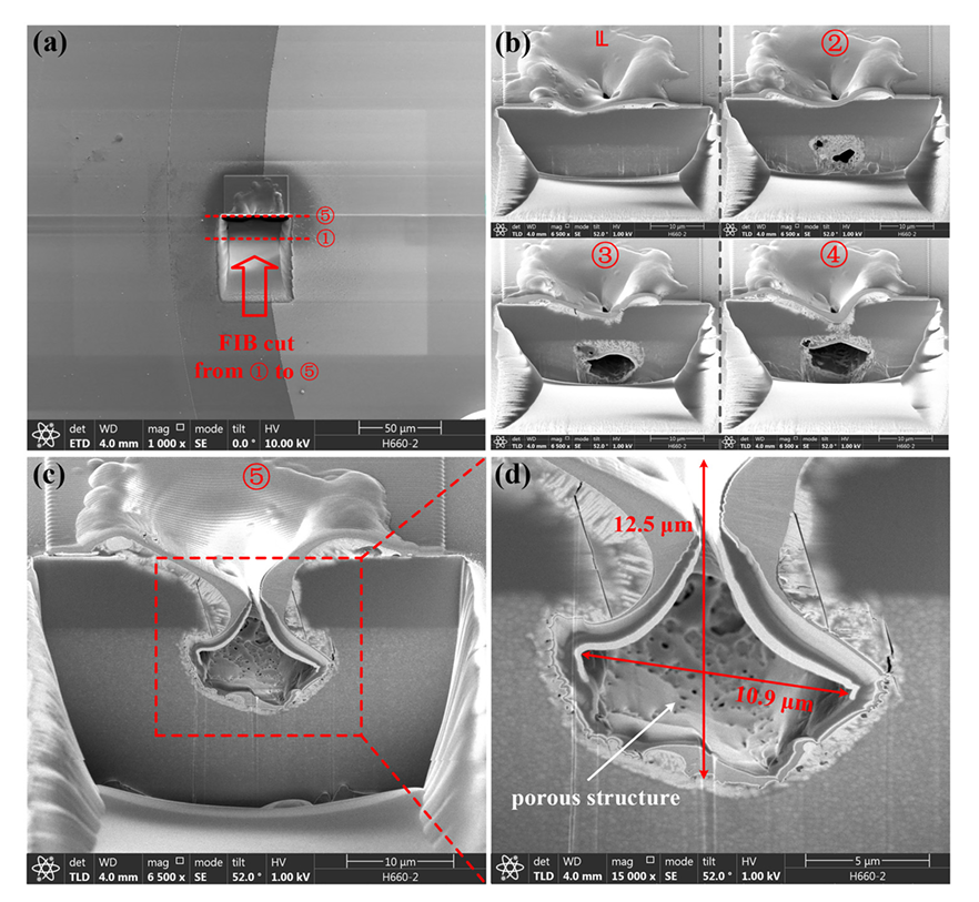
Fig. 3. (a) FIB-cut cross section of the failure region from position 1 to position 5. (b) and (c) Detailed cross-sectional images at positions ‹ to › during the FIB process. (d) Enlarged image of the burnout point.
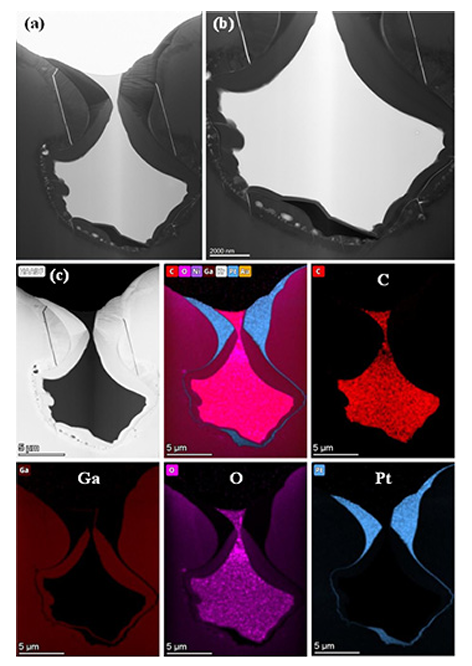
Fig. 4. (a) and (b) TEM images of the failure region. (c) Elemental distributions at the burnout point obtained by TEM-EDX mapping, including carbon, gallium, oxygen, and platinum.
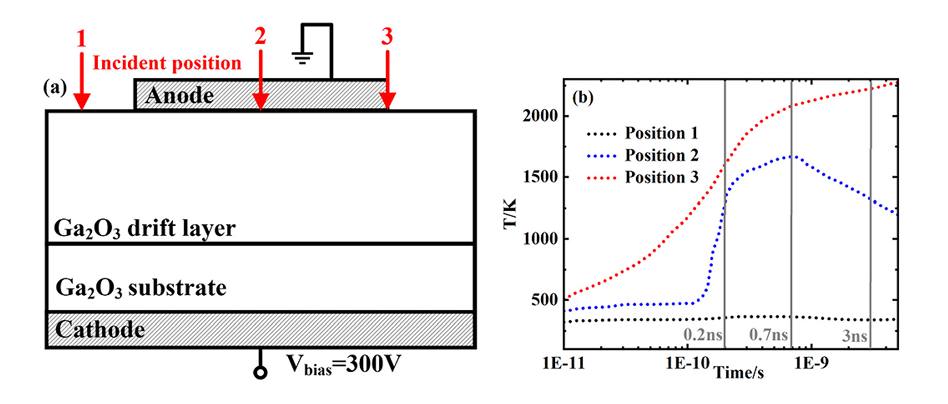
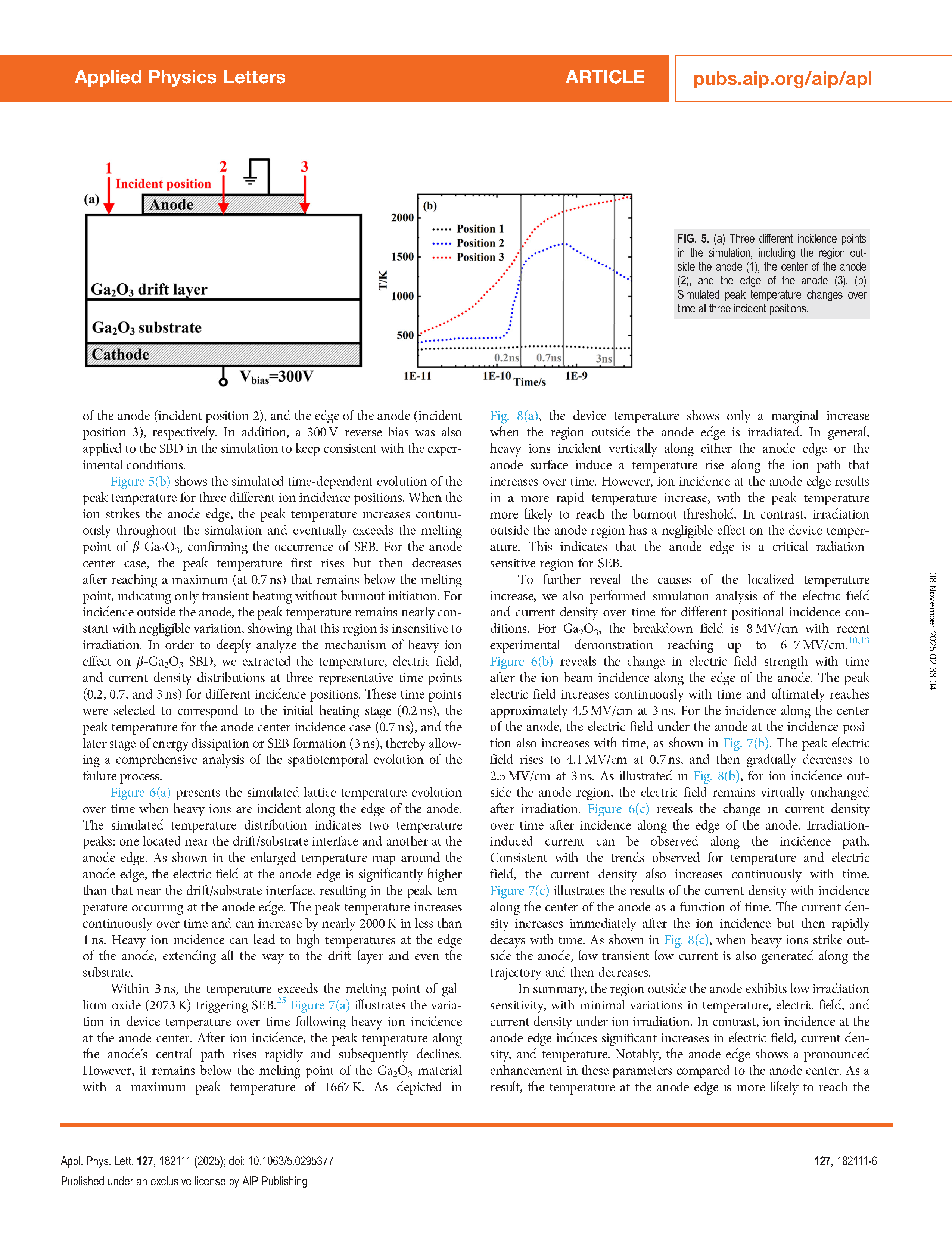
Fig. 5. (a) Three different incident points in the simulation, including the region outside the anode (1), the center of the anode (2), and the edge of the anode (3). (b) Simulated peak temperature variations over time at the three incident positions.

FIG. 6. Simulated (a) lattice temperature, (b) electric field, and (c) current density over time when heavy ions are incident along anode edge (incident position 3).
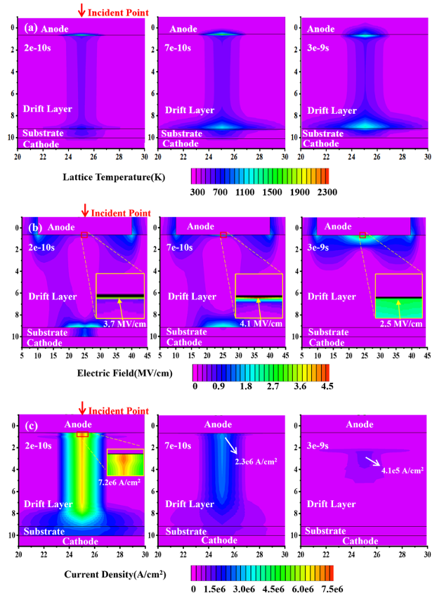
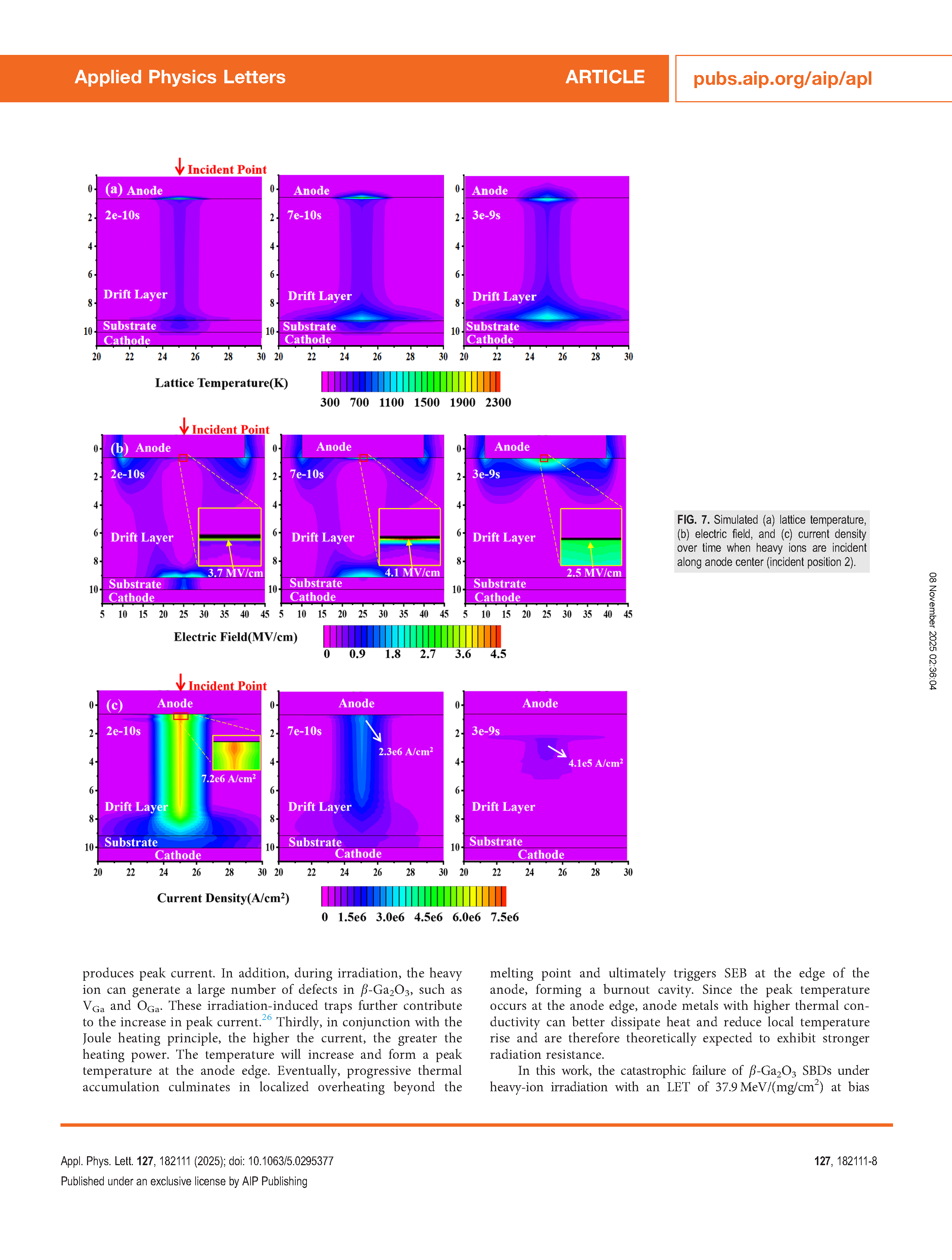
FIG. 7. Simulated (a) lattice temperature, (b) electric field, and (c) current density over time when heavy ions are incident along anode center (incident position 2).
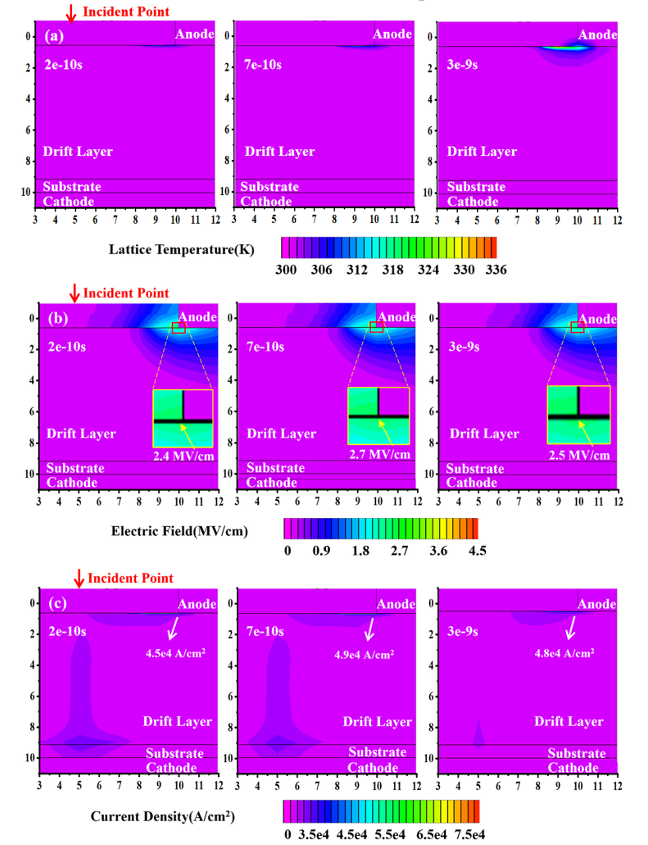
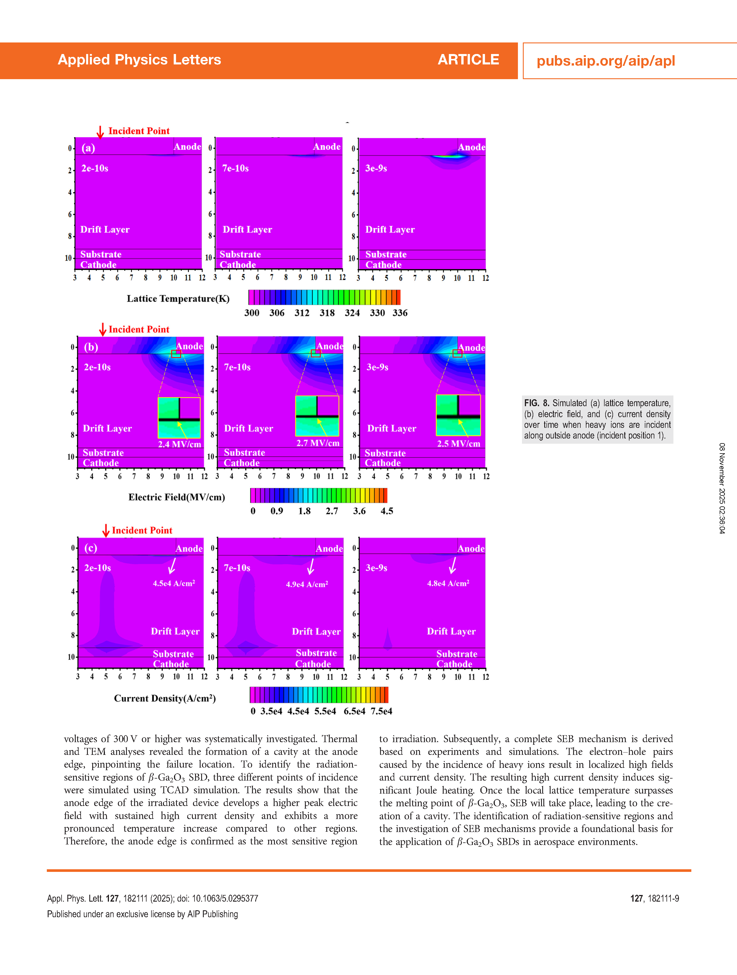
FIG. 8. Simulated (a) lattice temperature, (b) electric field, and (c) current density over time when heavy ions are incident along outside anode (incident position 1).
DOI:
doi.org/10.1063/5.0295377