Paper Sharing
【Member Papers】Low-temperature growth of β-Ga₂O₃ film on MgO (100) substrate by HVPE for solar-blind ultraviolet imaging photodetector array
日期:2025-11-25阅读:442
Researchers from the Tianjin University of Technology have published a dissertation titled "Low-temperature growth of β-Ga2O3 film on MgO (100) substrate by HVPE for solar-blind ultraviolet imaging photodetector array" in Journal of Alloys Compounds.
Project Support
This work was supported by the Major Project of Tianjin Science and Technology (Grant no. 18ZXJMTG00230), the Key Research and Development Program of Tianjin (Nos. 24YFXTHZ00200 and 24YFXTHZ00210) and Tianjin Municipal Enterprise Technology Commissioner Program (Nos. 25YDTPJC00350 and 25YDTPJC00310).
Background
The rapid development of wide-bandgap semiconductor materials has provided critical support for innovations in high-performance photodetection technologies. As an ultrawide-bandgap semiconductor (Eg ≈ 4.9 eV) featuring a high critical breakdown field of 8 MV/cm, excellent deep-UV transparency, and outstanding chemical stability, β-Ga₂O₃ has emerged as a core candidate material for deep-ultraviolet (UVC, 200–280 nm) photodetection. Its unique electronic band structure enables high responsivity and narrow spectral selectivity in the deep-UV region, effectively suppressing visible-light background interference and overcoming key limitations of conventional silicon-based detectors—namely, broad spectral response and high dark-current noise.
However, traditional β-Ga₂O₃ epitaxial growth techniques often require high-temperature conditions, which can induce increased crystal defect densities and aggravated lattice mismatch effects. These issues severely limit improvements in device optoelectronic performance and hinder the industrialization and large-scale fabrication of β-Ga₂O₃-based technologies.
Our breakthrough in low-temperature hydride vapor phase epitaxy (HVPE) provides an effective solution to this bottleneck. Through a low-temperature (~550 °C) vapor-phase deposition process, HVPE enables precise control of film composition and thickness, while offering advantages such as high growth rate (up to 2 μm/h), controllable fabrication cost, and compatibility with heterogeneous integration. These features make HVPE highly compatible with the intrinsic properties of β-Ga₂O₃.
Leveraging the synergistic benefits of HVPE and β-Ga₂O₃, the development of high-performance β-Ga₂O₃-based photodetectors and imaging arrays has become a research frontier in the wide-bandgap semiconductor field. Such devices not only achieve highly sensitive and rapid deep-UV detection but, through array-level integration, also meet the demands of applications including security monitoring, aerospace sensing, and industrial UV nondestructive inspection that require high-precision UV imaging. This provides key technological support for the industrial deployment and large-scale application of wide-bandgap semiconductor optoelectronic technologies.
Abstract
In this work, high-quality β-Ga₂O₃ films were heteroepitaxially grown on MgO (100) substrates via halide vapor phase epitaxy (HVPE), and high-sensitivity solar-blind ultraviolet photodetectors (SBUVPDs) as well as their array were fabricated. At the optimized growth temperature of 550 °C, single-phase, (100)-oriented β-Ga₂O₃ films were epitaxially grown on MgO (100) substrates, with an in-plane epitaxial relationship of β-Ga₂O₃ <021> // MgO <010>, and the surface roughness as low as 9.32 nm. The MSM-type SBUVPDs based on β-Ga₂O₃ (100)/MgO (100) film exhibited excellent optoelectronic performance, featuring ultra-low I₍dark₎ (8.43 pA), large I₍light₎/I₍dark₎ (1.11 × 10⁶), high responsivity (222.38 A/W), detectivity (4.4 × 10¹⁵ Jones), and external quantum efficiency (1.1 × 10³ %), along with a fast response speed to 254 nm UV light. The 5 × 4 SBUVPD array fabricated via lithography processes possessed high resolution, excellent responsivity uniformity with minimal deviation, and low color distortion imaging capabilities, making it suitable for optoelectronic imaging applications. In summary, our work validates that the HVPE method is suitable for the heteroepitaxial growth of β-Ga₂O₃ films on MgO (100) substrates and demonstrates the application of such films in fabricating high-performance devices such as SBUVPD arrays, which contributes to the development of wide-bandgap semiconductor-based optoelectronic imaging applications.
Conclusion
In this study, we successfully achieved heteroepitaxial growth of β-Ga₂O₃ films on MgO substrates using the HVPE method by modulating the growth zone temperature. The MSM-type photodetector fabricated from the β-Ga₂O₃ (100)/MgO (100) film grown at 550 ℃ demonstrated superior comprehensive performance in SBUV detection. Subsequently, we fabricated a 5 × 4 solar-blind ultraviolet photodetector array through photolithography for imaging applications. The photodetector array displayed uniform photo-response characteristics and captured images with low chromatic aberration. Our work not only provides valuable guidance for the design of imaging arrays, but also contributes to the advancement of wide-bandgap semiconductor photoelectric imaging applications, particularly for Ga₂O₃.
This work has notable limitations: various parameters influence the epitaxial growth quality of β-Ga₂O₃ films, although this paper concentrates solely on the critical variable of growth temperature. Furthermore, the performance of the photodetectors can be enhanced. In the future, we can systematically examine the regulatory patterns of additional growth parameters, conduct research on thin film doping, and investigate the practical application potential of photodetectors, facilitating the transition of laboratory findings to industrial applications.
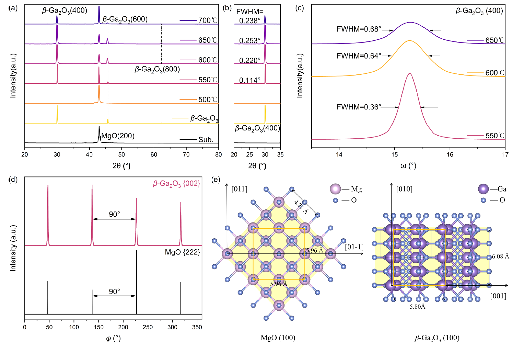
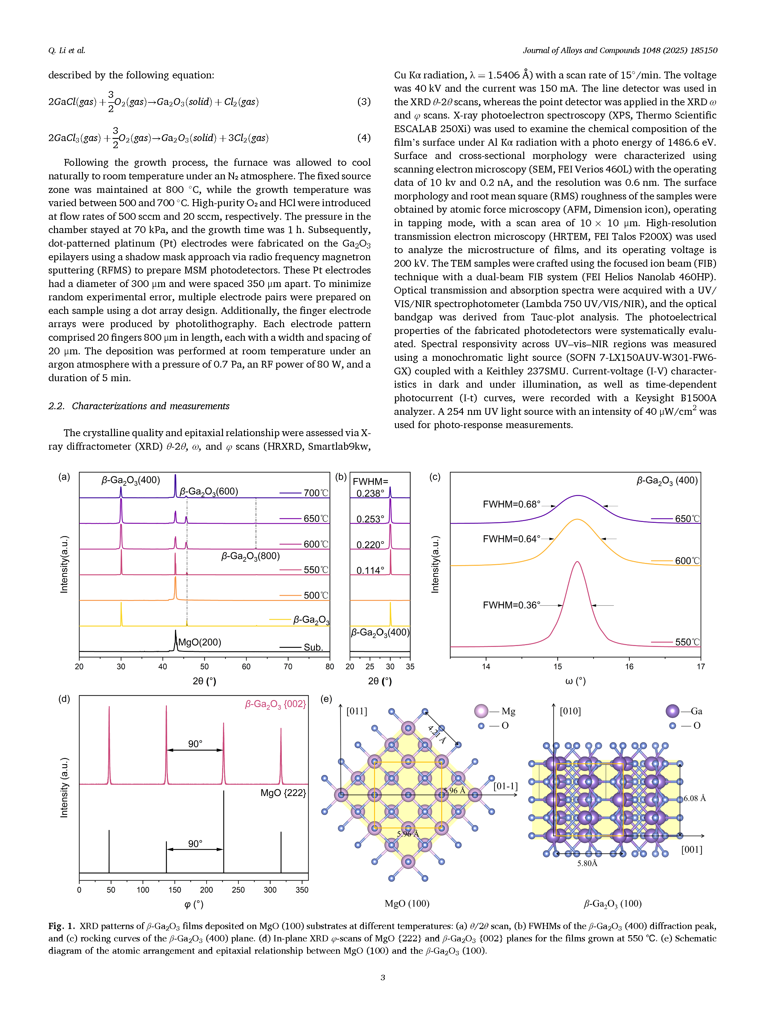
Fig. 1. XRD patterns of β-Ga₂O₃ films deposited on MgO (100) substrates at different temperatures: (a) θ/2θ scan, (b) FWHMs of the β-Ga₂O₃ (400) diffraction peak, and (c) rocking curves of the β-Ga₂O₃ (400) plane. (d) In-plane XRD φ-scans of MgO {222} and β-Ga₂O₃ {002} planes for the films grown at 550 ℃. (e) Schematic diagram of the atomic arrangement and epitaxial relationship between MgO (100) and the β-Ga₂O₃ (100).
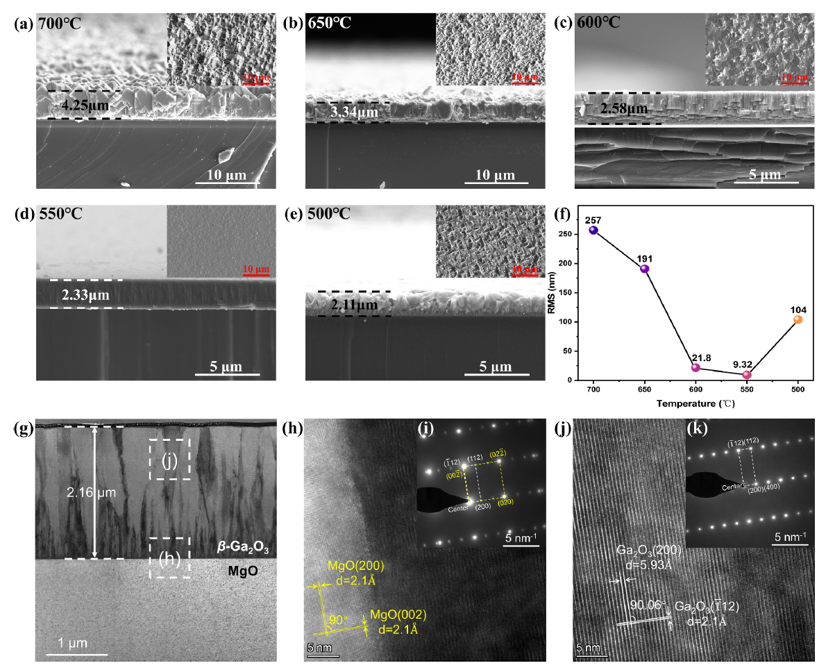
Fig. 2. SEM images of cross-sections and surfaces (inset) of the β-Ga₂O₃ epilayers grown at different temperatures: (a) 700 ℃; (b) 650 ℃; (c) 600 ℃; (d) 550 ℃; (e) 500 ℃. (f) The RMS roughness of β-Ga₂O₃ films with temperature variation. TEM images of the β-Ga₂O₃ film deposited at 550 ℃: (g) Low-resolution TEM image. (h–k) High-resolution TEM image of the film (j), substrate and their interface (h), and the SAED patterns of the corresponding interface (i) and film (k).
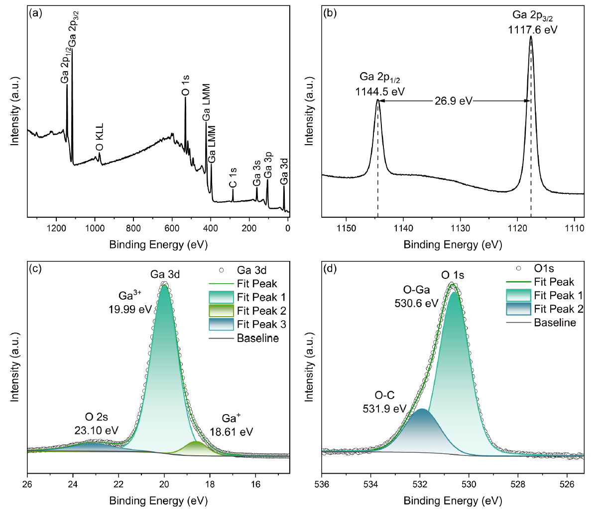
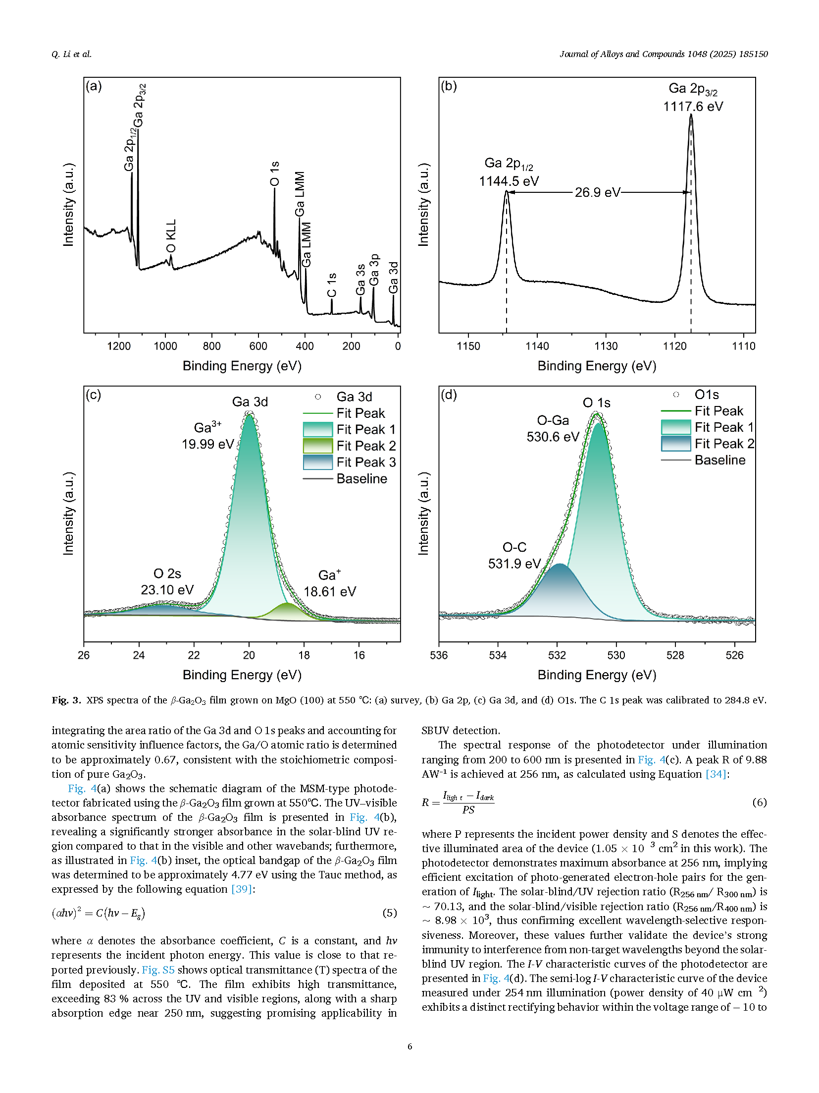
Fig. 3. XPS spectra of the β-Ga₂O₃ film grown on MgO (100) at 550 ℃: (a) survey, (b) Ga 2p, (c) Ga 3d, and (d) O 1s. The C 1s peak was calibrated to 284.8 eV.
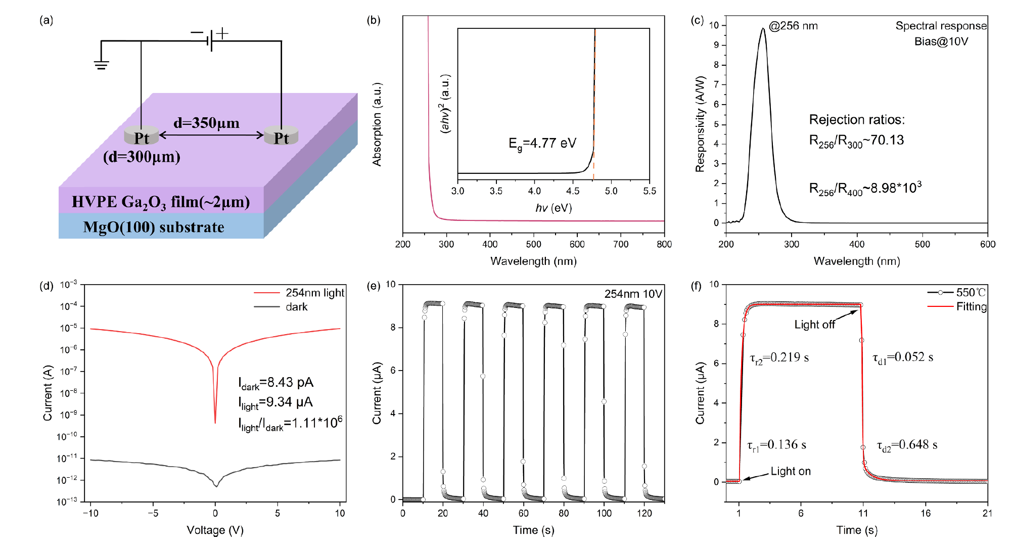
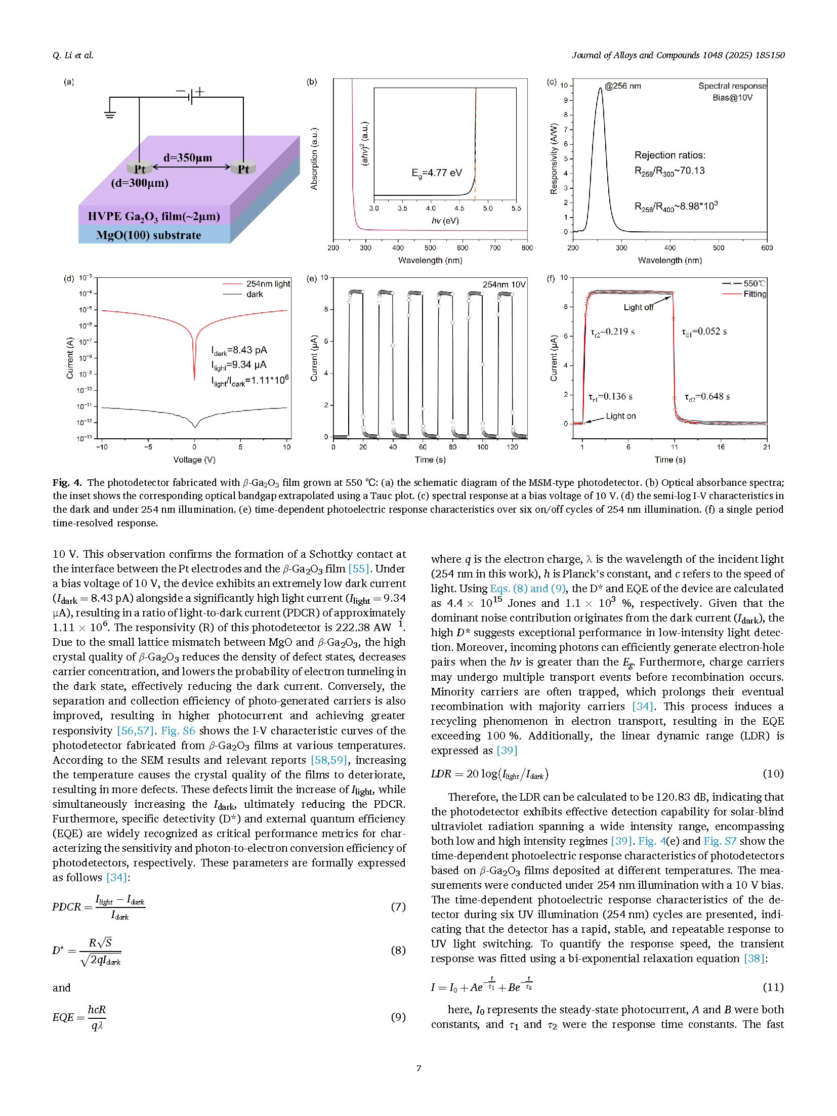
Fig. 4. The photodetector fabricated with β-Ga₂O₃ film grown at 550 ℃: (a) the schematic diagram of the MSM-type photodetector. (b) Optical absorbance spectra; the inset shows the corresponding optical bandgap extrapolated using a Tauc plot. (c) Spectral response at a bias voltage of 10 V. (d) The semi-log I–V characteristics in the dark and under 254 nm illumination. (e) Time-dependent photoelectric response characteristics over six on/off cycles of 254 nm illumination. (f) A single period time-resolved response.
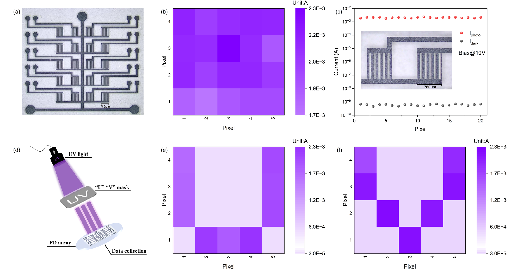
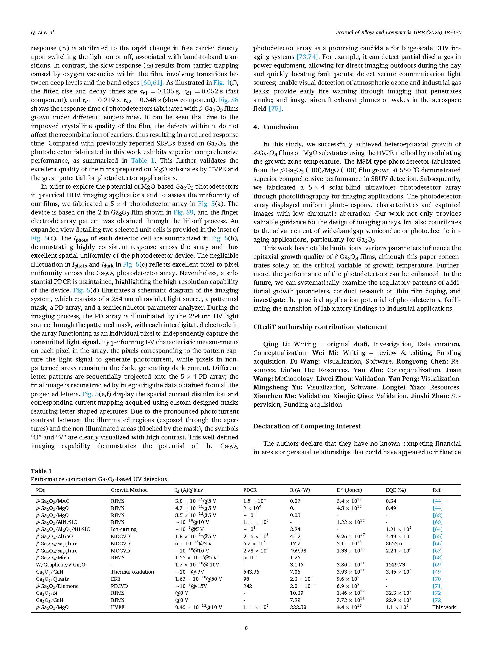
Fig. 5. (a) Layout of photodetector array; (b) the photocurrent distribution; and (c) dark current and photocurrent for all pixels within the array; the inset shows the enlarged portion of (a). (d) The schematic diagram of the SBUV imaging system, and (e,f) corresponding imaging results of the ‘U’ ‘V’ pattern under 254 nm illumination.
DOI:
doi.org/10.1016/j.jallcom.2025.185150