Paper Sharing
【Member Papers】Heterogeneous integration of ultrawide bandgap semiconductors for radio frequency power devices
日期:2025-11-24阅读:593
Researchers from the Xidian University have published a dissertation titled "Heterogeneous integration of ultrawide bandgap semiconductors for radio frequency power devices" in Science Advances.
Project Suppot
The work in Xidian University was supported by the National Natural Science Foundation of China (NSFC) with the grant nos. 62222407 and 62421005 (to H.Z.).
Background
Radio-frequency (RF) semiconductor devices are widely used in communication, consumer electronics, aerospace, and defense applications, with design goals typically including high cutoff frequency, high maximum oscillation frequency, high output power density, high efficiency, and low noise. Wide bandgap (WBG) and ultrawide bandgap (UWBG) semiconductors, owing to their large bandgap, high critical electric field, and high saturation velocity, are considered key materials for enhancing RF device performance. However, a single UWBG material rarely offers both shallow-level dopants and high thermal conductivity—for example, Ga₂O₃ has low thermal conductivity, whereas AlN and diamond possess high thermal conductivity but lack shallow-level dopants—limiting device output power and reliability.
Heterogeneous integration of different UWBG materials offers a promising solution to this challenge. Existing approaches, including mechanical exfoliation, hydrogen ion cutting, and wafer bonding, enable material combination but face limitations such as restricted flake size, material degradation, and high interfacial thermal resistance. In this work, we develop a novel heterogeneous integration technique that combines mechanical exfoliation, arrayed transfer, and wafer-level direct bonding. This approach ensures good film uniformity and enables large-area arrays, providing a new pathway for the fabrication of high-performance RF devices and integrated circuits.
Abstract
Ultrawide bandgap (UWBG) semiconductors offer high critical electric fields and saturation velocities ideal for radio frequency (rf) devices, but achieving both shallow-level doping and high thermal conductivity (kT) in a single material remains difficult. We demonstrate a scalable, exfoliation-based layer-transfer process to heterogeneously integrate gallium oxide (Ga2O3) thin films with shallow dopants onto high-kT aluminum nitride (AlN) substrates. This method obviates ion implantation and interfacial dielectric layers used in conventional approaches. A large conduction band offset (3.4 electron volts) at the Ga2O3/AlN interface improves electron confinement in the Ga2O3 channel. T-gate rf power transistors achieve a maximum oscillation frequency of 90 gigahertz and output power densities of 4.6 watts per millimeter at 2 gigahertz and 4.1 watts per millimeter at 6 gigahertz—among the highest for UWBG devices. A minimal noise figure of 0.48 decibels at 8 gigahertz—among the lowest reported in this frequency range—further highlights the platform’s promise for next-generation rf applications.
Conclusion
In summary, this work presents a Ga2O3-on-AlN heterogeneously integrated platform for rf power devices, which can leverage the complementary electrical and thermal properties of multiple UWBG materials. The integration method combines exfoliated transfer and wafer-scale bonding, obviating the ion implantation and interfacial oxide required in many conventional methods, at the same time enabling a uniform geometry of the arrayed thin films with the total size scalable to the wafer level. The Ga2O3-on-AlN rf transistor leverages the high potential barrier offered by the AlN/Ga2O3 junction to realize tight gate control and gate length scalability in a highly doped Ga2O3 channel. In addition, the high EC of the AlN substrate eliminates the premature substrate breakdown. These synergistic advances in the material, process, and device enable impressive frequency and power performance, including an average electric field over 3 MV/cm, a fT/fmax of 23.8/90 GHz, a Pout of 4.1 to 4.6 W/mm at 2 to 6 GHz, and a NFmin of 0.48 dB at 8 GHz, with the Pout being the highest in all UWBG rf devices and the noise among the one of the lowest in all representative X-band rf devices. These results suggest great potential of the heterogeneous UWBG platform for high-frequency, high-power, and low-noise rf electronics.
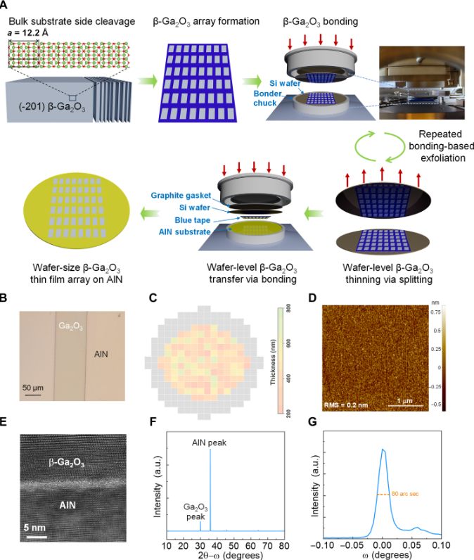
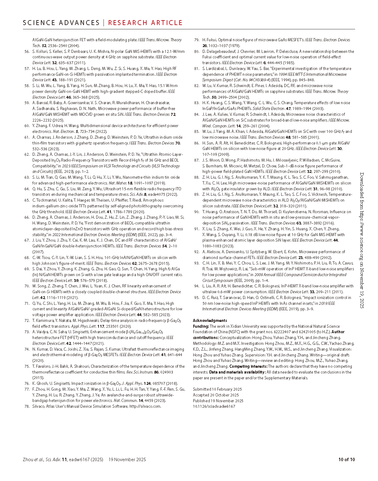
Fig. 1. Heterogeneous integration process and material characterization.(A) Illustration of the Ga2O3/AlN heterogeneous integration process. The β-Ga2O3 belt or film with uniform geometry is cleaved from the substrate edge and then manually transferred onto the blue tape to form an array. The thickness of β-Ga2O3 films on blue tape is reduced by multiple wafer-level bonding process until the thickness reaches around 500 nm. The graphite/Si/β-Ga2O3/AlN stack is formed and loaded into the bonding chamber under a 3-hour bonding process to transfer the wafer-size β-Ga2O3 film array onto the AlN substrate. (B) Top-view optical microscopic image of part of a single β-Ga2O3 film on the AlN substrate. (C) Thickness mapping of 120 β-Ga2O3 films in a wafer-size array after being transferred onto the 1-inch AlN substrate. (D) Atomic force microscopy (AFM) image of the surface of β-Ga2O3 film transferred on the AlN substrate, revealing an atomic flat surface with an RMS roughness of 0.2 nm. (E) Zoomed-in and HRTEM image at the atomic interface between the β-Ga2O3 channel and AlN substrate. (F) XRD scan characteristics of β-Ga2O3 on AlN. a.u., arbitrary units. (G) High-resolution rocking curve of transferred and bonded β-Ga2O3 with an FWHM of 80 arc sec.
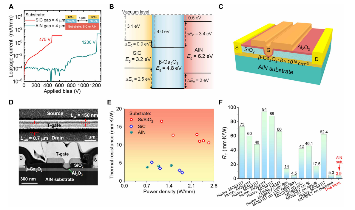
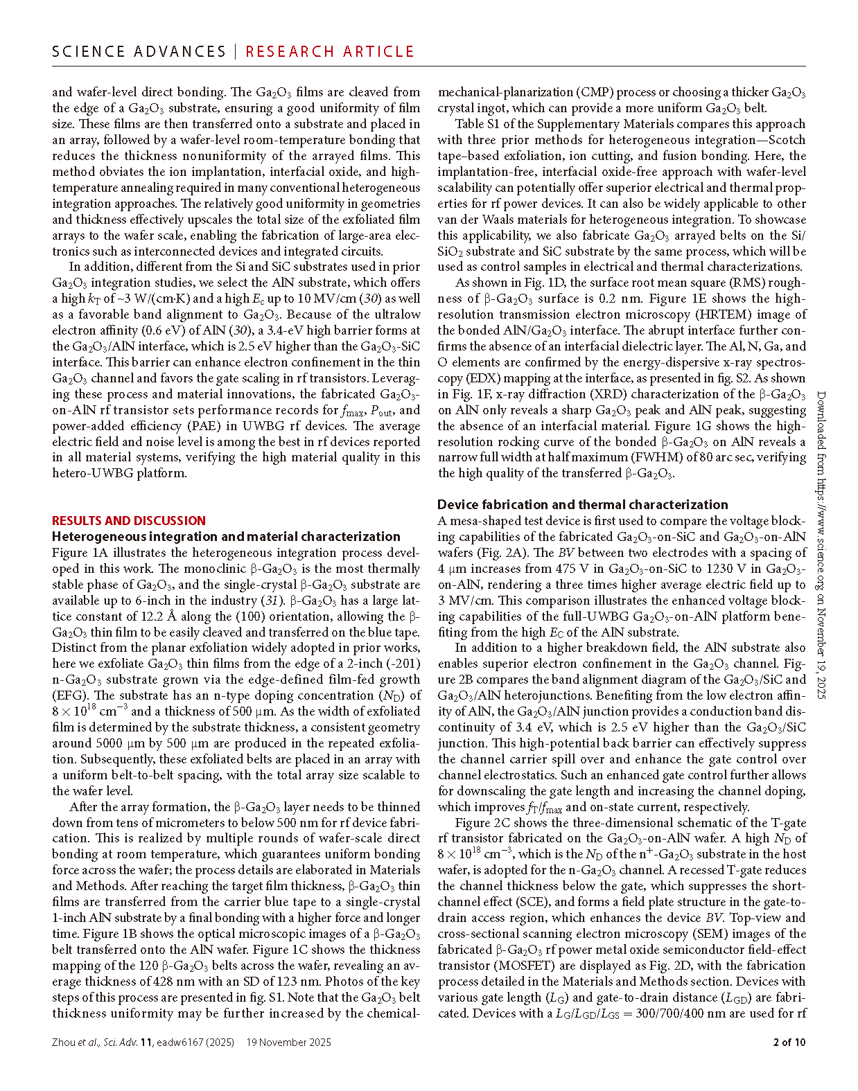
Fig. 2. Electrical and thermal properties of the hetero-UWBG platform and device design.(A) Leakage current characteristics between two mesa structures fabricated on the β-Ga2O3 on the AlN sample and the β-Ga2O3 on the SiC sample, revealing a 2.5 times higher breakdown voltage in the β-Ga2O3 on the AlN sample. (B) Band alignment of SiC, β-Ga2O3, and AlN, where a large conduction band discontinuity of 3.4 eV is presented between β-Ga2O3 and AlN. (C) Cross-sectional schematic image of β-Ga2O3 rf power MOSFETs on the AlN substrate. (D) Top-view SEM and cross-sectional TEM images of a T-gate shaped β-Ga2O3 rf power MOSFET with LG = 150 nm and a gated channel thickness of 30 nm. (E) Extracted thermal resistance (RT) versus dc power density of identical-geometry Ga2O3 MOSFETs fabricated on SiO2/Si, SiC, and AlN substrates; the same heterogeneous integration process is applied to three substrates. (F) RT benchmark for this work and other reported Ga2O3 transistors on a variety of substrates.
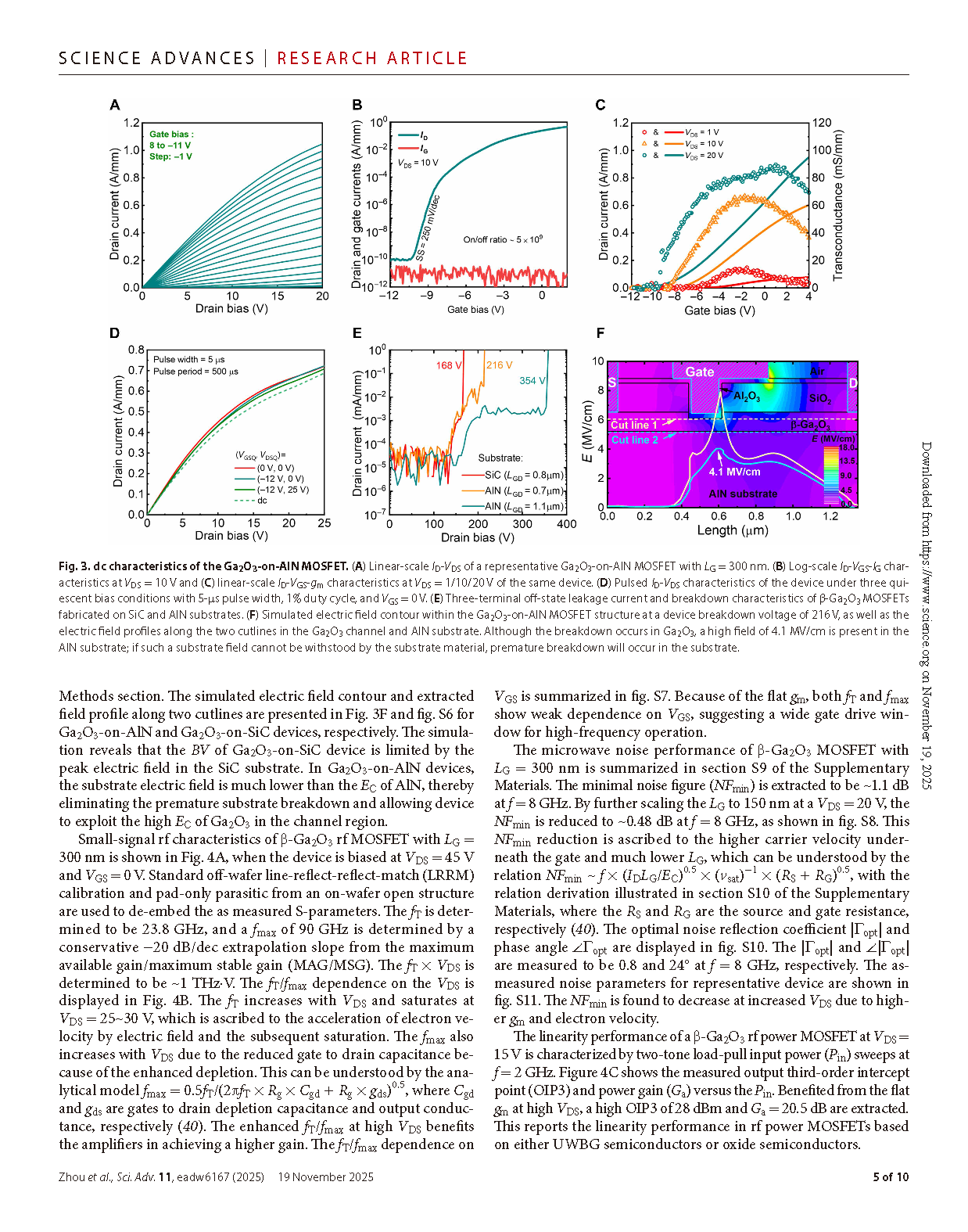
Fig. 3. dc characteristics of the Ga2O3-on-AlN MOSFET.(A) Linear-scale ID-VDS of a representative Ga2O3-on-AlN MOSFET with LG = 300 nm. (B) Log-scale ID-VGS-IG characteristics at VDS = 10 V and (C) linear-scale ID-VGS-gm characteristics at VDS = 1/10/20 V of the same device. (D) Pulsed ID-VDS characteristics of the device under three quiescent bias conditions with 5-μs pulse width, 1% duty cycle, and VGS = 0 V. (E) Three-terminal off-state leakage current and breakdown characteristics of β-Ga2O3 MOSFETs fabricated on SiC and AlN substrates. (F) Simulated electric field contour within the Ga2O3-on-AlN MOSFET structure at a device breakdown voltage of 216 V, as well as the electric field profiles along the two cutlines in the Ga2O3 channel and AlN substrate. Although the breakdown occurs in Ga2O3, a high field of 4.1 MV/cm is present in the AlN substrate; if such a substrate field cannot be withstood by the substrate material, premature breakdown will occur in the substrate.
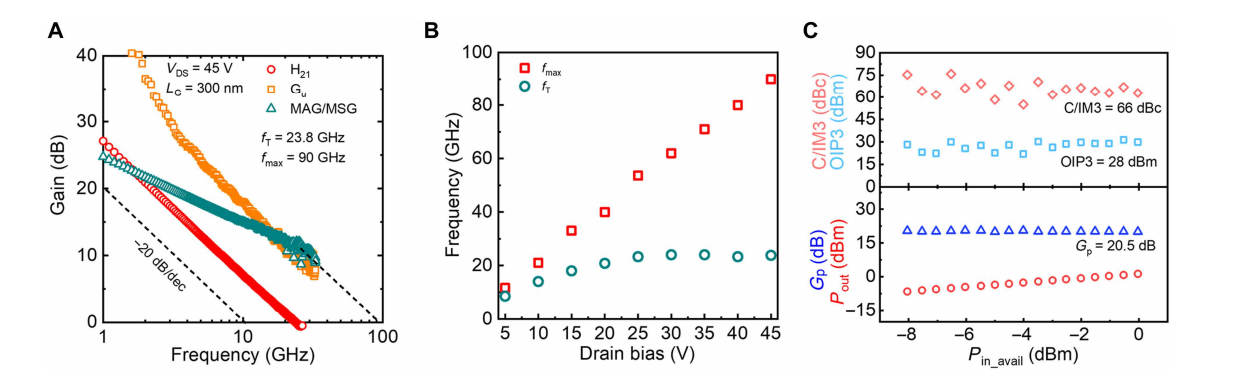
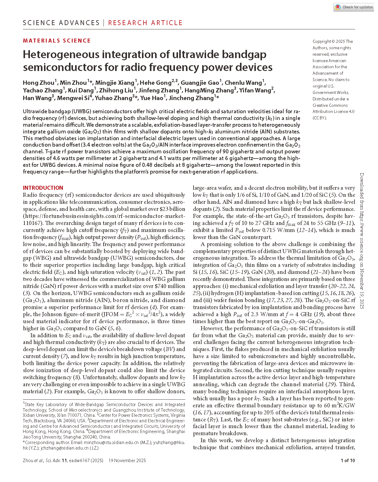
Fig. 4. Small-signal rf characteristics and linearity characteristics of the Ga2O3-on-AlN MOSFET.(A) Small-signal gain characteristics of a Ga2O3-on-AlN MOSFET with LG = 300 nm when biased at VDS = 45 V and at the VGS corresponding to the peak gm and (B) extracted fT and fmax versus VDS. A fmax = 90 GHz is extracted. (C) Two-tone load-pull Pin sweeps at f = 2 GHz to study the linearity of a device at VDS = 15 V. A high linearity with OIP3 = 28 dBm is extracted.
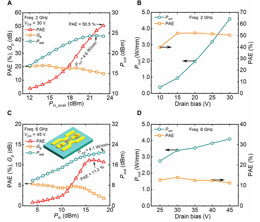
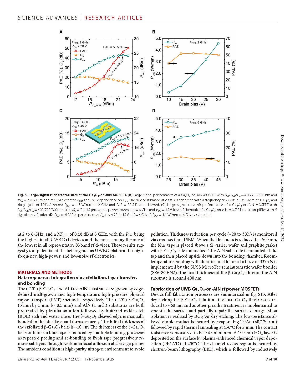
Fig. 5. Large-signal rf characteristics of the Ga2O3-on-AlN MOSFET.Large-signal performance of a Ga2O3-on-AlN MOSFET with LGS/LGD/LG= 400/700/300 nm and WG = 2 × 30 μm and the (B) extracted Pout and PAE dependence on VDS. The device is biased at class-AB condition with a frequency of 2 GHz, pulse width of 100 μs, and duty cycle of 10%. A record Pout = 4.6 W/mm at 2 GHz and PAE = 50.5% are achieved. (C) Large-signal class-AB performance of a Ga2O3-on-AlN MOSFET with LGS/LGD/LG = 400/700/300 nm and WG = 2 × 15 μm, with a power sweep at f = 6 GHz and VDS = 45 V. Inset: Schematic of a Ga2O3-on-AlN MOSFET for an amplifier with rf signal amplification (D) Pout and PAE dependence on VDS from 25 to 45 V at f = 6 GHz. A Pout = 4.1 W/mm at 6 GHz is extracted.
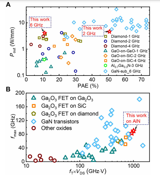
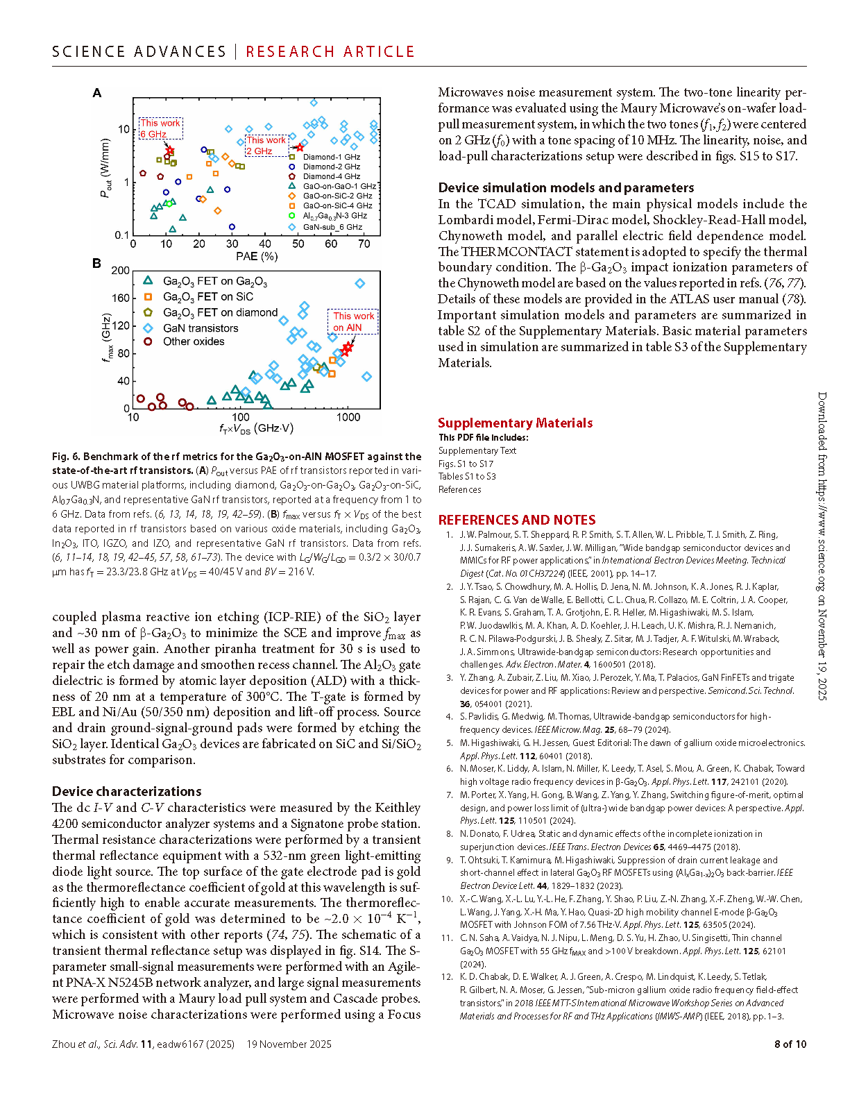
Fig. 6. Benchmark of the rf metrics for the Ga2O3-on-AlN MOSFET against the state-of-the-art rf transistors. Poutversus PAE of rf transistors reported in various UWBG material platforms, including diamond, Ga2O3-on-Ga2O3, Ga2O3-on-SiC, Al7Ga0.3N, and representative GaN rf transistors, reported at a frequency from 1 to 6 GHz. (B) fmax versus fT × VDS of the best data reported in rf transistors based on various oxide materials, including Ga2O3, In2O3, ITO, IGZO, and IZO, and representative GaN rf transistors. The device with LG/WG/LGD = 0.3/2 × 30/0.7 μm has fT = 23.3/23.8 GHz at VDS = 40/45 V and BV = 216 V.
DOI:
doi.org/10.1126/sciadv.adw6167