Paper Sharing
【Member Papers】Optical properties of 2 inch β-Ga₂O₃ crystals grown by the vertical Bridgman method
日期:2025-11-23阅读:430
Researchers from the Zhejiang University have published a dissertation titled "Optical properties of 2 inch β-Ga2O3 crystals grown by the vertical Bridgman method" in Semiconductor Science and Technology.
Project Support
This work was supported by the National Key Research and Development Program of China (2024YFE0205300), ‘Pioneer’ and ‘Leading Goose’ R&D Program of Zhejiang (2023C01193), the National Natural Science Foundation of China (22205203), the Natural Science Foundation of Zhejiang (LZ25E070001), the National Program for Support of Topnotch Young Professionals and the Leading Innovative and Entrepreneur Team Introduction Program of Hangzhou (TD2022012).
Background
Recent advances in β-Ga2O3-based high-voltage/high-frequency electronics have demonstrated the exceptional potential of this ultrawide bandgap (4.8 eV) semiconductor, with its remarkable theoretical breakdown field strength of 8 MV cm−1 and superior Baliga figure of merit of 3444 relative to Si for unipolar devices. The feasibility of growing β-Ga2O3 bulk single crystals from melts enables cost-effective production compared with SiC and GaN. Multiple methods have been developed to grow bulk β-Ga2O3 single crystal, including the Czochralski (CZ) technique, edge-defined film-fed growth (EFG), casting, the optical floating-zone (OFZ) method and oxide crystal growth from a cold crucible. However, these methods face inherent challenges in balancing cost, scalability and crystal quality. The OFZ method is capable of producing high-purity β-Ga2O3 at reduced cost, while the crystal diameters are typically limited to a few millimeters by the light spot. Conversely, CZ and EFG methods have achieved crystal growth up to 6 inches and casting has achieved crystal growth up to 8 inches, even though they suffer from loss of the expensive Ir crucible and the associated Ir contamination.
Abstract
β-Ga2O3, an ultrawide bandgap semiconductor (4.8 eV, 8 MV cm−1 breakdown field), is vital for high-voltage electronics. This study employs the vertical Bridgman (VB) method with Pt–Rh crucibles to grow 2 inch <010>-oriented single crystals (unintentionally doped, Sn/Fe-doped), addressing the cost and scalability issues of conventional techniques. X-ray diffraction shows high crystallinity (full width at half maximum ∼20 arcsec, ⩽7% variation). Sn-doped samples exhibit uniform resistivity (2 × 10⁻² Ω · cm) via Ga vacancy-mediated diffusion. Spectroscopy reveals that passive Rh doping behavior induces a 0.05–0.09 eV bandgap extension and a 2.9 eV absorption threshold, while reducing the Fermi level–valence band maximum separation by 0.34 eV. The VB technique provides a scalable, low-cost pathway for industrial production of high-quality β-Ga2O3 substrates, offering critical insights into the effects of Rh doping that advance strategies for p-type conductivity and next-generation power device applications.
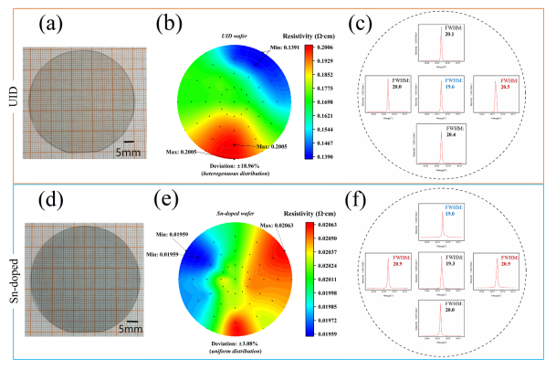
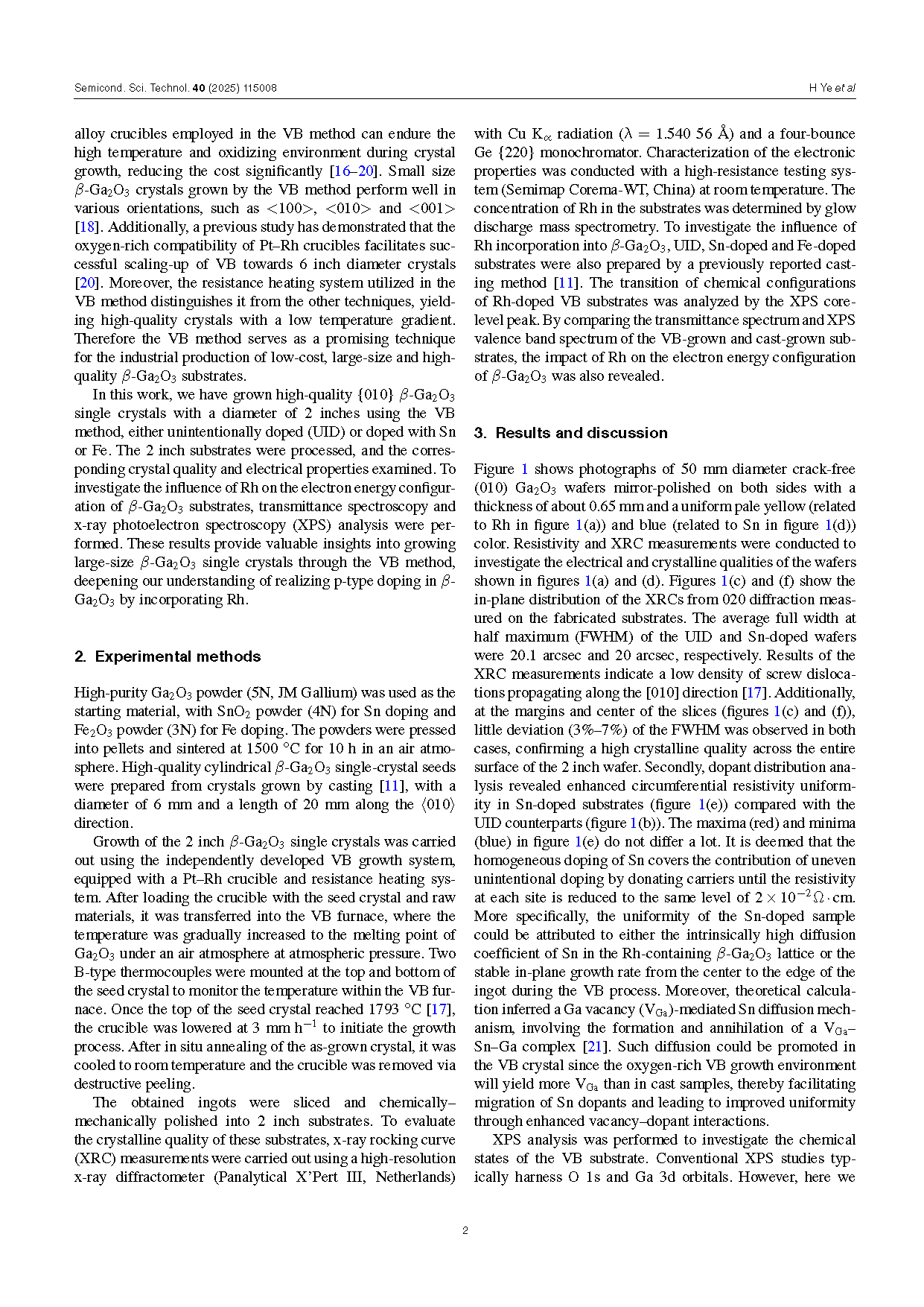
Figure 1. Photographs of polished 2 inch (a) UID and (d) Sn-doped {010} β-Ga2O3 substrates grown by the VB method, with the corresponding in-plane distribution diagram of (b), (e) resistivity (Ωcm) and (c), (f) FWHM of the 020 diffraction rocking curve.
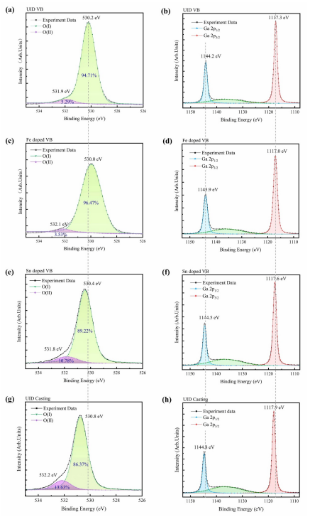
Figure 2. XPS spectra of O 1s and Ga 2p peaks of (a), (b) UID VB, (c), (d) Fe doped VB, (e), (f) Sn doped VB and (g), (h) UID casting β-Ga2O3 samples, respectively. Fitting results are filled with colors.
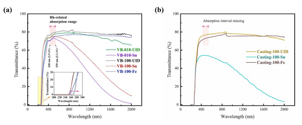
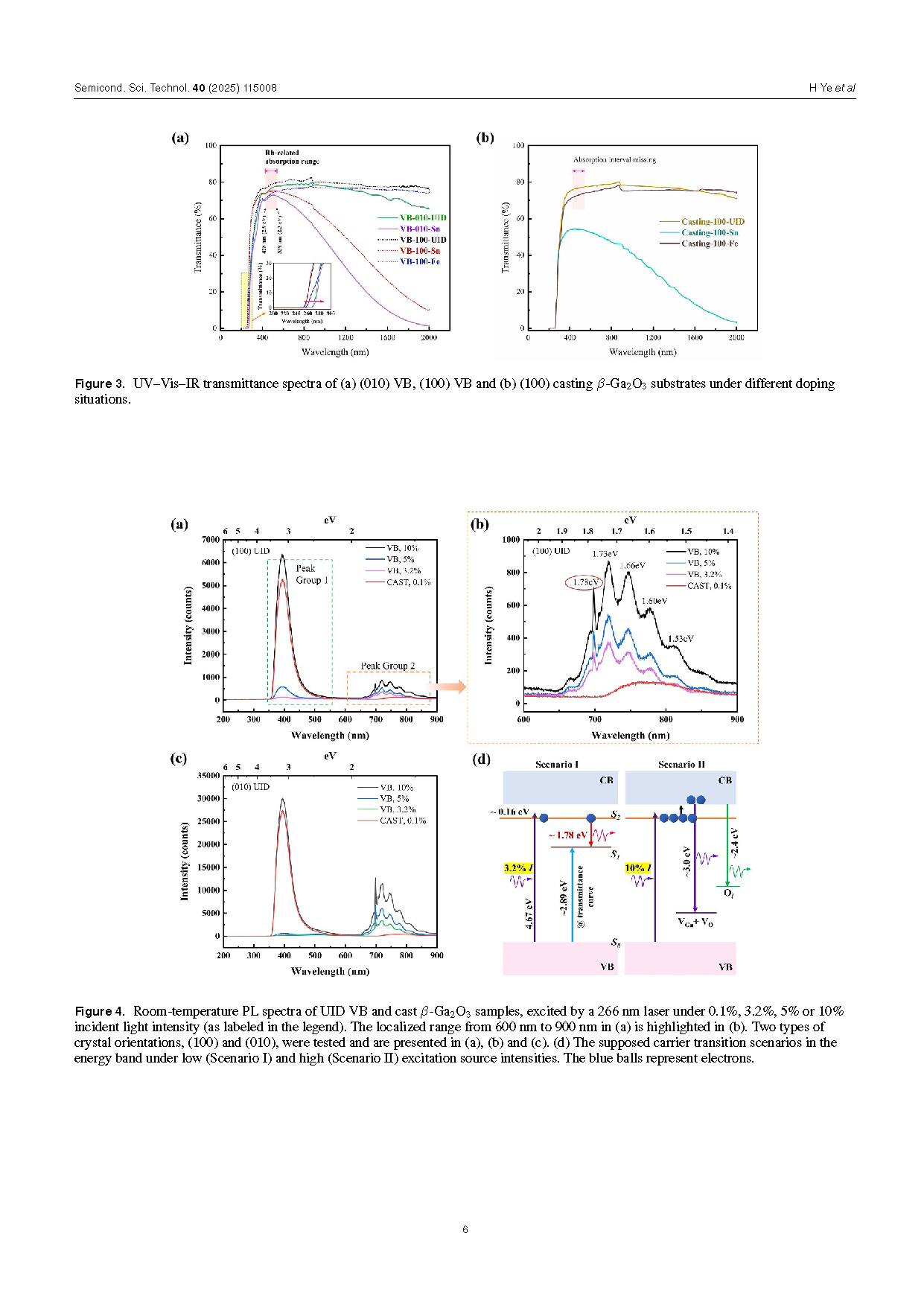
Figure 3. UV–Vis–IR transmittance spectra of (a) (010) VB, (100) VB and (b) (100) casting β-Ga2O3 substrates under different doping situations.
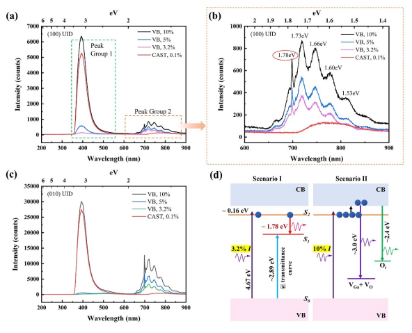
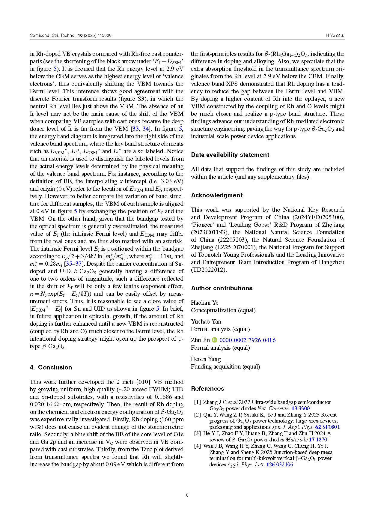
Figure 4. Room-temperature PL spectra of UID VB and cast β-Ga2O3 samples, excited by a 266 nm laser under 0.1%, 3.2%, 5% or 10% incident light intensity (as labeled in the legend). The localized range from 600 nm to 900 nm in (a) is highlighted in (b). Two types of crystal orientations, (100) and (010), were tested and are presented in (a), (b) and (c). (d) The supposed carrier transition scenarios in the energy band under low (Scenario I) and high (Scenario II) excitation source intensities. The blue balls represent electrons.
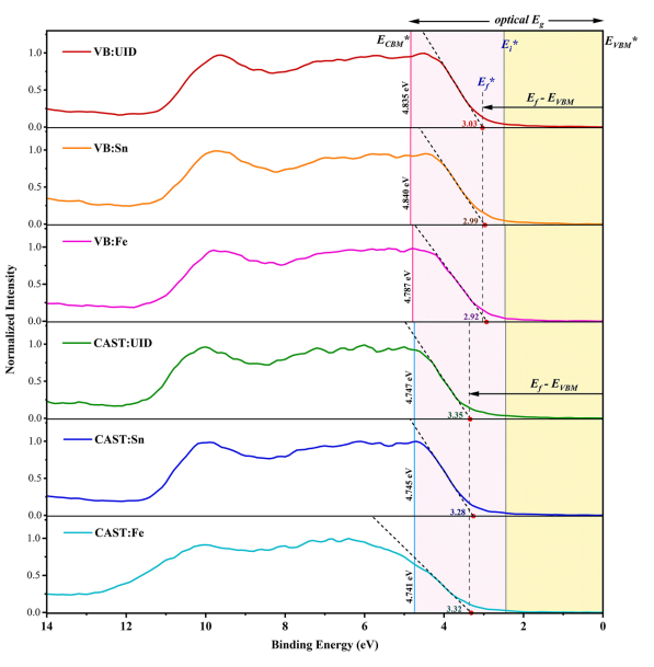
Figure 5. Valence band XPS spectra of a (100) substrate grown by VB and casting methods. The colored blocks (pink and orange) represent the energy band diagram.
DOI:
doi.org/10.1088/1361-6641/ae0e47