Paper Sharing
【International Papers】Surface dipole formation and electronic structure evolution on β-Ga₂O₃
日期:2025-11-23阅读:495
Researchers from the King Abdullah University of Science and Technology and University of Wisconsin-Madison have published a dissertation titled " Surface dipole formation and electronic structure evolution on β-Ga2O3" in Applied Physics Letters.
Background
Ultra-wide bandgap semiconductors have emerged as promising materials for next-generation power electronics, deep-ultraviolet optoelectronics, and extreme-environment sensing, among which β-Ga₂O₃ has attracted significant attention due to its wide bandgap (4.6–5 eV), high breakdown electric field (8 MV/cm), and availability of large-area single-crystal substrates. Among its various crystallographic orientations, the (010) surface exhibits higher electron mobility, making it suitable for high-power and high-frequency applications, whereas the (-201) surface is thermodynamically the most stable, favoring heteroepitaxial growth; both orientations thus serve as robust platforms for high-performance device fabrication. To improve surface cleanliness, stoichiometry, and interface quality, various surface treatments have been employed, including HF, HCl, H₂O₂, ultraviolet/ozone, and CF₄/O₂ plasma treatments, with Piranha solution (H₂SO₄:H₂O₂) widely used to remove organic residues and promote oxygen-rich terminations, significantly enhancing the interface quality of ALD-Al₂O₃/β-Ga₂O₃ and reducing interface trap densities. However, the evolution of β-Ga₂O₃ surface electronic structures following treatment, including work function, surface band bending, and vacuum level alignment, and their impact on interface behavior, remain inadequately understood. While ultraviolet photoelectron spectroscopy (UPS) can probe work functions and valence band structures, it cannot provide core-level information; in contrast, X-ray photoelectron spectroscopy (XPS) under negative sample bias allows simultaneous measurement of work function, core levels, and valence band maximum, ensuring internal consistency and providing a reliable basis for constructing accurate surface band diagrams. In this work, Piranha-treated (-201) and (010) β-Ga₂O₃ surfaces were systematically investigated using in situ Ar⁺ ion sputtering combined with XPS to quantify surface stoichiometry, Ga–OH groups, oxygen vacancies, and surface energy band structures. The results reveal a dipole-driven mechanism governing the pronounced reduction in work function, providing new insights into β-Ga₂O₃ surface behavior and strategies for interface engineering in Ga₂O₃-based electronic devices.
Conclusion
In summary, we systematically explored the surface electronic structure of β-Ga₂O₃ with (−201) and (010) orientations following Piranha treatment, using in situ XPS with stepwise Ar⁺ ion etching. This approach enabled clear separation of vacuum level bending from conduction/valence band bending. Piranha treatment generated an oxygen-rich surface layer that introduced asymmetric charge distribution and inward-pointing dipoles, leading to a substantial vacuum level shift [0.93 eV for (−201), 0.89 eV for (010)] and a reduced work function. As the dipolar layer was etched away, the vacuum level shifted upward, while surface band bending and Ga–OH concentration concurrently decreased. Core-level shifts (~0.2 eV) were minor compared to the vacuum shift, confirming that dipole formation is the primary mechanism governing the initial low work function. These findings offer critical insight into the electronic structure of Ga₂O₃ surfaces and highlight opportunities for band alignment engineering and interface optimization in Ga₂O₃-based electronic and optoelectronic devices.
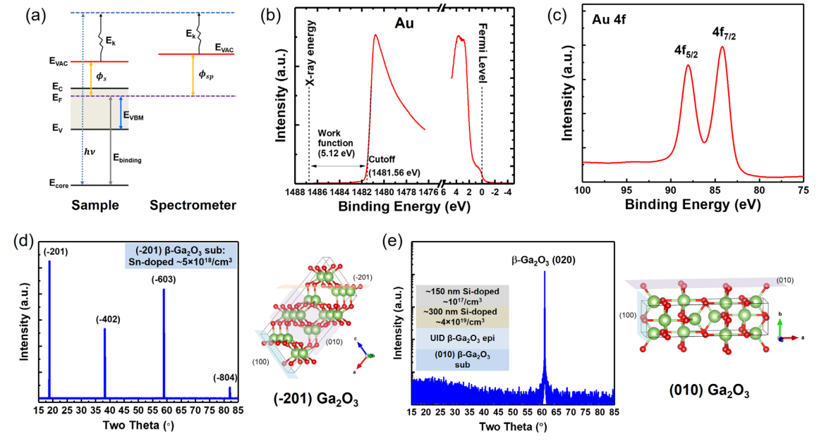
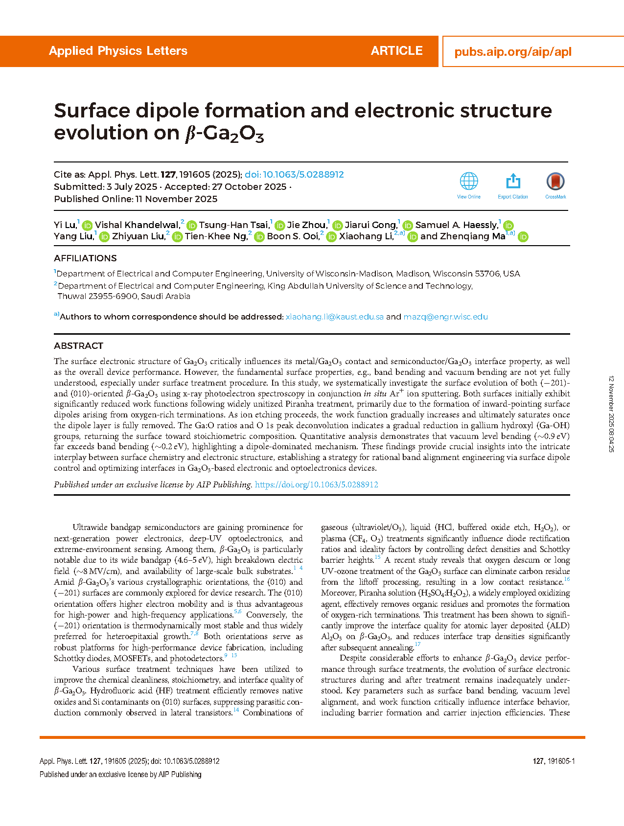
FIG. 1. (a) Schematic of surface work function (Φₛ) extraction via secondary electron cutoff (SECO) in XPS. (b) XPS spectrum of a standard Au sample showing SECO and Fermi edge. (c) Au 4f spectrum. (d) XRD 2θ–ω scan of Sn-doped β-Ga₂O₃ (−201) single crystal. (e) XRD 2θ–ω scan of epitaxial β-Ga₂O₃ (010) film on (010) substrate. VESTA-rendered atomic models of β-Ga₂O₃ (−201) and (010) surfaces are shown in (d) and (e).
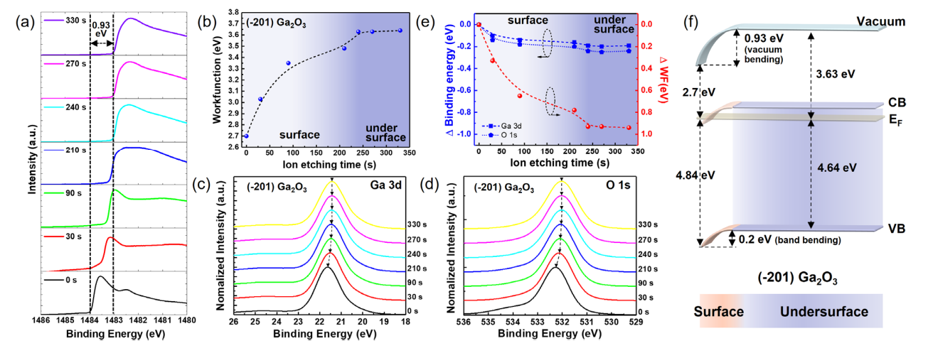
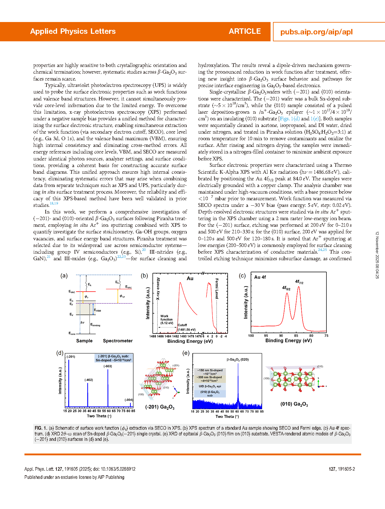
FIG. 2. Depth-dependent surface electronic structure of (−201) β-Ga₂O₃. (a) In situ evolution of SECO spectra measured at various Ar⁺ sputtering times. (b) Extracted work function from (a). (c) and (d) Normalized Ga 3d and O 1s core-level spectra. (e) Binding energy shifts of Ga 3d and O 1s (left axis) and work function shift ΔΦₛ (right axis) relative to the initial (0 s) state. (f) Reconstructed energy band diagram of the (−201) surface. The conduction band (CB) is shown assuming the surface and subsurface bandgaps are the same, as the surface bandgap cannot be directly measured.
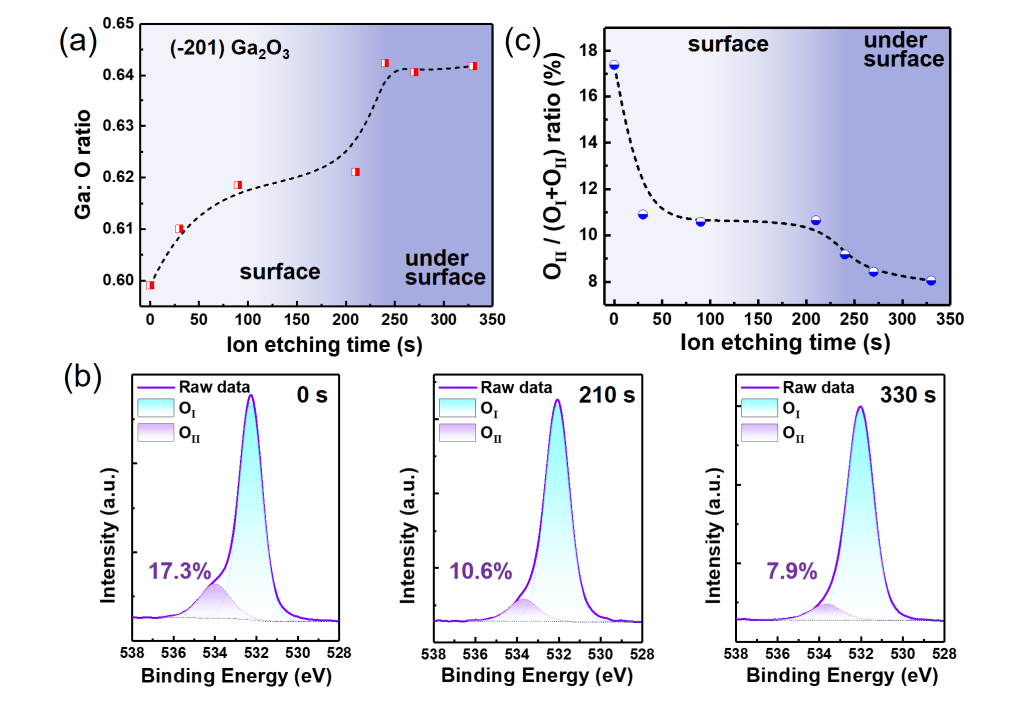
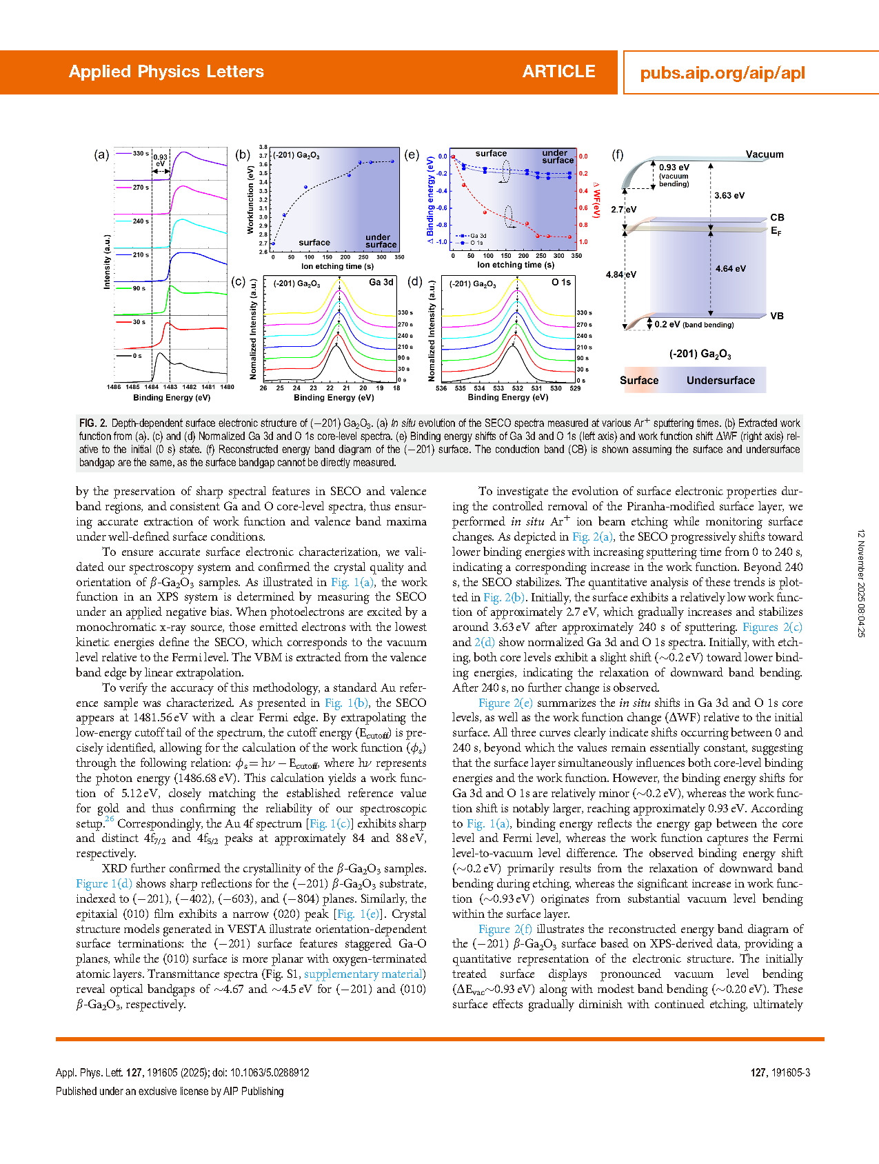
FIG. 3. Depth-dependent surface chemical composition of (−201) β-Ga₂O₃. (a) Evolution of Ga:O atomic ratio as a function of Ar⁺ etching time. (b) Fitted O 1s spectra at 0, 210, and 330 s. (c) OII / (OI + OII) ratio as a function of etching time.
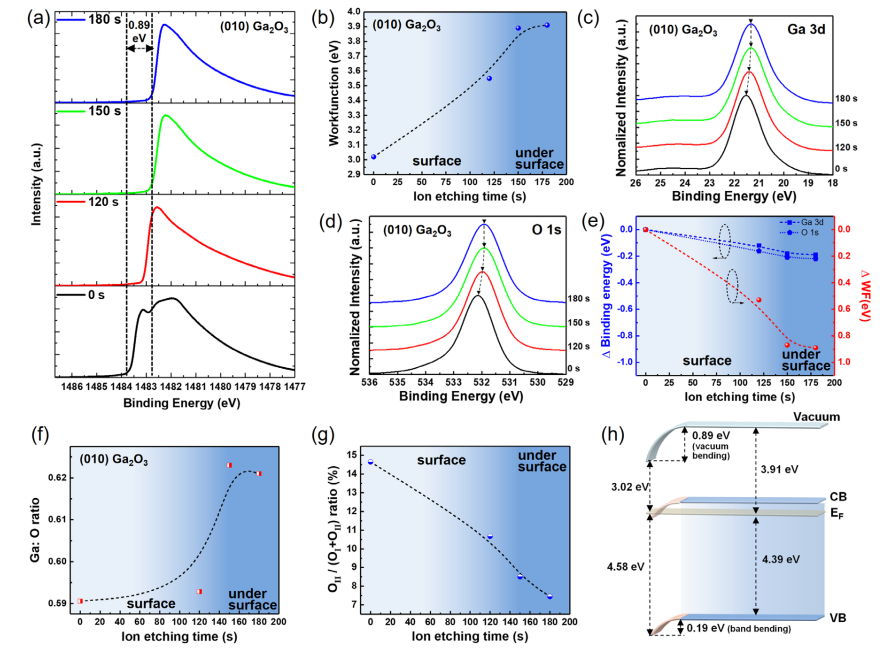
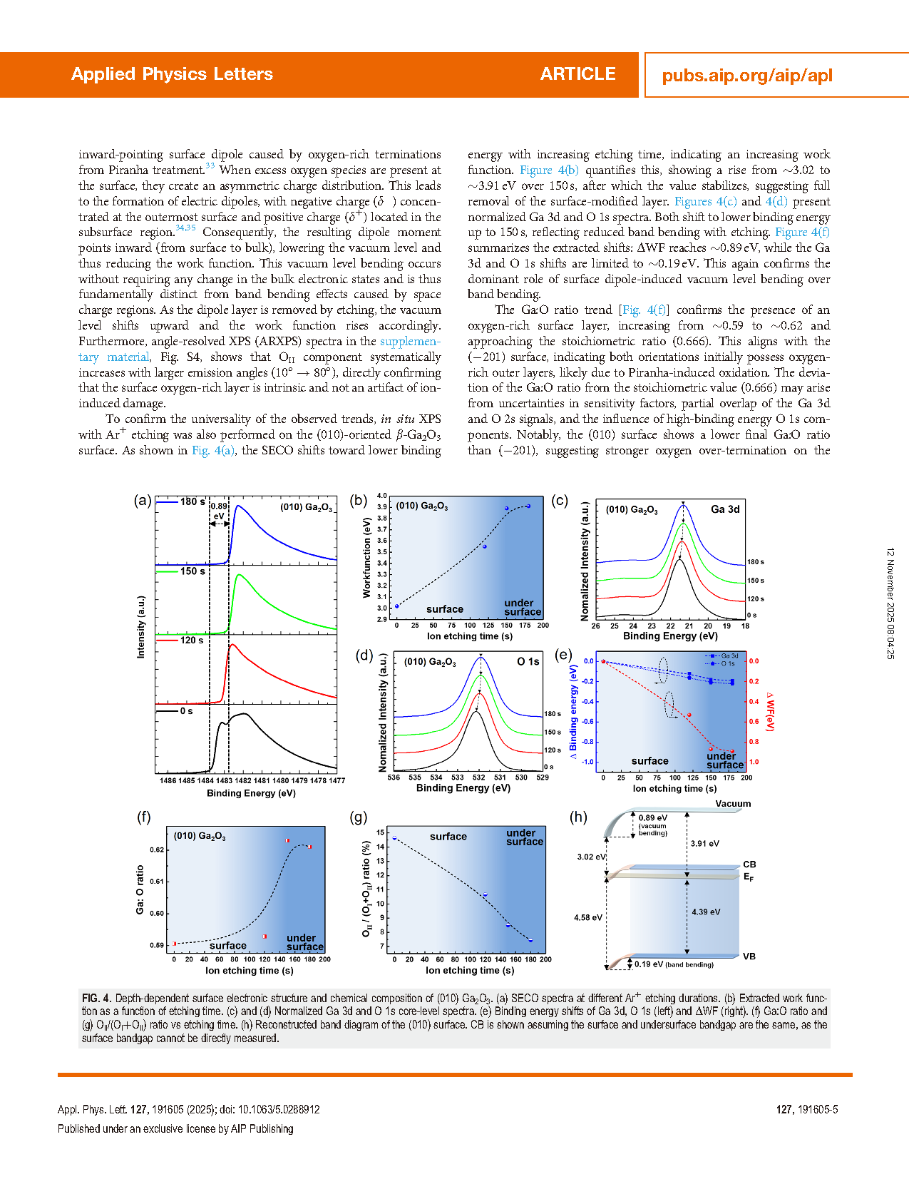
FIG. 4. Depth-dependent surface electronic structure and chemical composition of (010) β-Ga₂O₃. (a) SECO spectra measured at different Ar⁺ etching durations. (b) Extracted work function as a function of etching time. (c) and (d) Normalized Ga 3d and O 1s core-level spectra. (e) Binding energy shifts of Ga 3d and O 1s (left axis) and work function shift ΔΦₛ (right axis). (f) Ga:O atomic ratio and (g) OII / (OI + OII) ratio as a function of etching time. (h) Reconstructed energy band diagram of the (010) surface. The conduction band (CB) is shown assuming the surface and subsurface bandgaps are the same, as the surface bandgap cannot be directly measured.
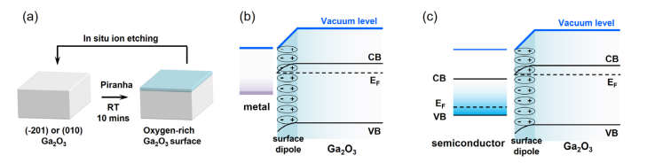
FIG. 5. (a) Schematic of the Piranha treatment and Ar⁺ ion etching sequence for surface modification. (b) Illustration of a metal/β-Ga₂O₃ interface. (c) Illustration of a semiconductor/β-Ga₂O₃ heterojunction incorporating oxygen-rich termination.
DOI:
doi.org/10.1063/5.0288912