Paper Sharing
【International Papers】P-type LiᵧNi₁₋ₓ₋ᵧMgₓO: A promising ultrawide bandgap semiconductor for Ga₂O₃ power devices applications
日期:2025-11-23阅读:442
Researchers from the Sejong University have published a dissertation titled "P-type LiyNi1-x-yMgxO: A promising ultrawide bandgap semiconductor for Ga2O3 power devices applications" in Journal of Magnesium and Alloys.
Background
Ultrawide-bandgap (UWBG) semiconductors have attracted significant interest for next-generation power devices due to their high breakdown voltage, excellent thermal stability, and energy efficiency. β-Ga₂O₃, an n-type UWBG semiconductor with a bandgap of ~4.9 eV, high critical electric field, and tunable doping, shows great potential for high-power switching applications. However, the lack of stable p-type conductivity limits the development of complementary devices. Various p-type candidates, such as CuAlO₂, CuGaO₂, and NiO, face challenges including low hole concentration, poor mobility, or high turn-on voltage. Li-doped Ni₁₋ₓMgₓO (LiyNi₁₋ₓ₋yMgₓO) offers tunable bandgap, controllable hole density and mobility, and good band alignment with β-Ga₂O₃, making it a promising p-type UWBG semiconductor for high-performance power devices.
Abstract
Ultrawide bandgap (UWBG) semiconductors are essential for the next generation of power electronics, offering superior breakdown voltages, thermal stability, and energy efficiency compared to conventional materials. However, the absence of efficient p-type UWBG semiconductors has been a major challenge, limiting the development of complementary devices. In this study, we explored LiyNi1-x-yMgxO as a potential p-type UWBG semiconductor, employing co-sputtering techniques to precisely control the Mg content by adjusting the power density applied to Mg target. X-ray diffraction (XRD) revealed enhanced (200) and (111) diffraction peaks with increasing Mg content, confirming successful incorporation of Mg into the NiO lattice. X-ray photoelectron spectroscopy (XPS) further validated the substitution of Ni by Mg atoms. As the Mg target power density increased from 0 to 1 W·cm-2, the optical bandgap widened from 4.27 eV to 5.44 eV, with corresponding improvements in optical transmittance. Hall effect measurements indicated a decrease in hole concentration with a significant enhancement in hole mobility as Mg content increased and reached 33.39 cm2V-1s-1 for 17.80 % Mg fraction. Despite the higher Mg fraction increasing the band alignment with n-type β-Ga2O3, a reduction in turn-on voltage with increasing Mg fraction compared with Li-doped NiO/β-Ga2O3 heterojunction diode (HJD) and an impressive BV of -1450 V were observed for films containing 17.80 % Mg. Silvaco TCAD simulations attributed these variations to trap-assisted tunneling, likely facilitated by Mg-induced energy levels within the Li-doped NiO matrix, which contributed to the reduction in turn-on voltage. The favorable electrical and optical properties of LiyNi1-x-yMgxO films, along with the successful integration of LiyNi1-x-yMgxO with β-Ga2O3 for heterojunction devices, demonstrate that LiyNi1-x-yMgxO is a promising candidate for future p-type materials in UWBG power device applications, particularly in conjunction with n-type β-Ga2O3 and other UWBG semiconductors.
Highlights
● Ultrawide bandgap p-type LiyNi1-x-yMgxO thin films were successfully demonstrated for power device integration.
● The optical bandgap was tunable from 4.27 eV to 5.44 eV by adjusting the Mg fraction in LiyNi1-x-yMgxO.
● A high hole mobility of 33.39 cm²V⁻¹s⁻¹ was achieved at 17.80 % Mg concentration.
● A LiyNi1-x-yMgxO/β-Ga₂O₃ heterojunction with a clean and well-defined interface was successfully demonstrated.
● A breakdown voltage of ∼1450 V was obtained for the heterojunction diode using 17.80 % Mg in LiyNi1-x-yMgxO.
● The turn-on voltage decreased with increasing Mg content, enhancing carrier injection at the interface.
Conclusion
In this study, we investigated a novel p-type ultrawide-bandgap (UWBG) compound semiconductor, LiyNi1-x-yMgxO, synthesized via co-sputtering with varying Mg content, for application in β-Ga2O3-based power devices. Structural analysis revealed that the intensities of the (200) and (111) XRD diffraction peaks increased with Mg content, correlating with the Mg target power. X-ray photoelectron spectroscopy (XPS) showed that Mg atoms successfully substituted Ni sites in the crystal lattice, as evidenced by changes in the O1s–Ni/O1s–Mg and Ni2p/Mg2p signals.
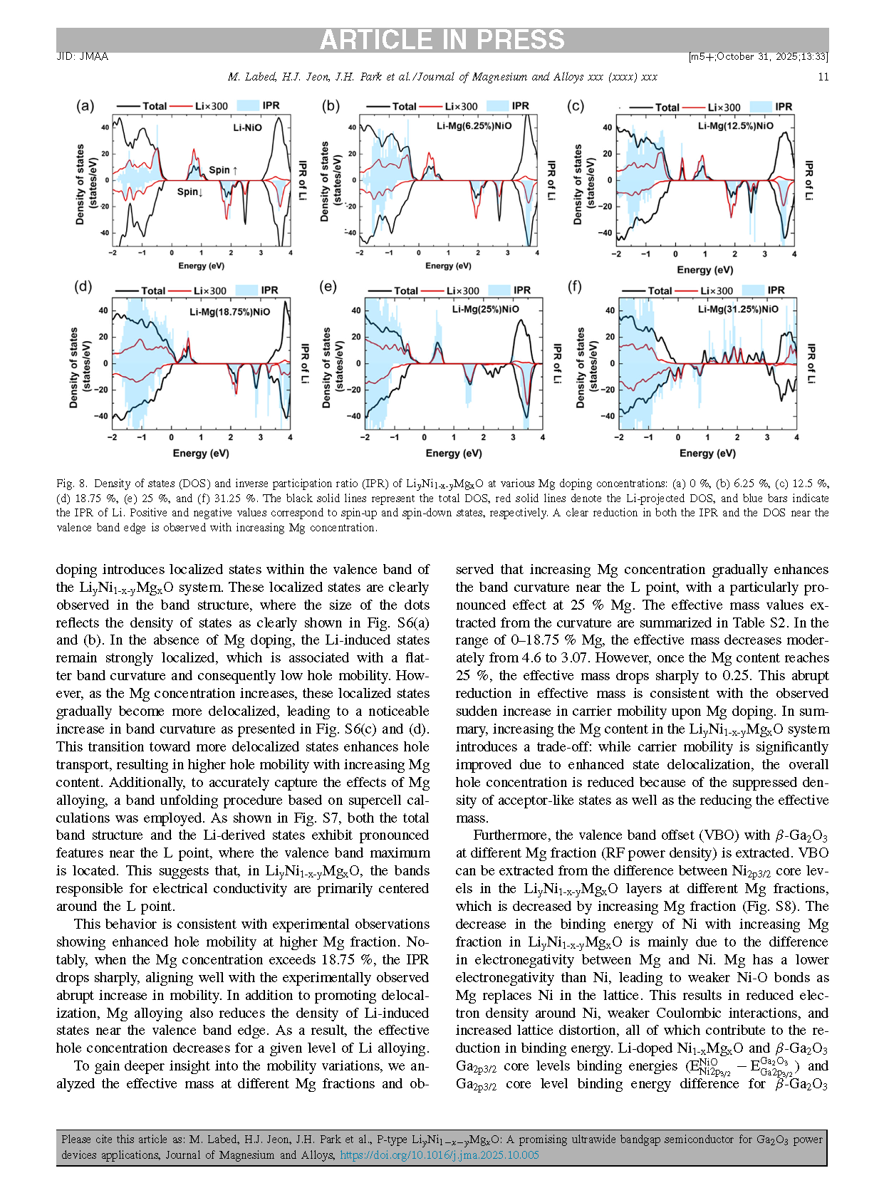
High-resolution transmission electron microscopy (HRTEM) confirmed a polycrystalline film structure at the LiyNi1-x-yMgxO/β-Ga2O3 interface, revealing crystallographic orientation, interplanar spacing, and the formation of an interfacial layer. Optical measurements showed a linear bandgap increase from 4.27 eV to 5.44 eV as Mg target power increased from 0 to 1 W·cm⁻², accompanied by enhanced optical transmittance compared to Li-doped NiO. Hall effect measurements indicated that hole concentration decreased from 1.72 × 10¹⁸ cm⁻³ (0% Mg) to 10¹⁶ cm⁻³ at an Mg fraction of ~17.80%, while hole mobility improved dramatically from 0.798 cm²V⁻¹s⁻¹ to 33.39 cm²V⁻¹s⁻¹. Density functional theory (DFT) calculations using VASP attributed this enhancement to a reduction in the inverse participation ratio (IPR) of valence band edge states, indicating increased delocalization of hole states.
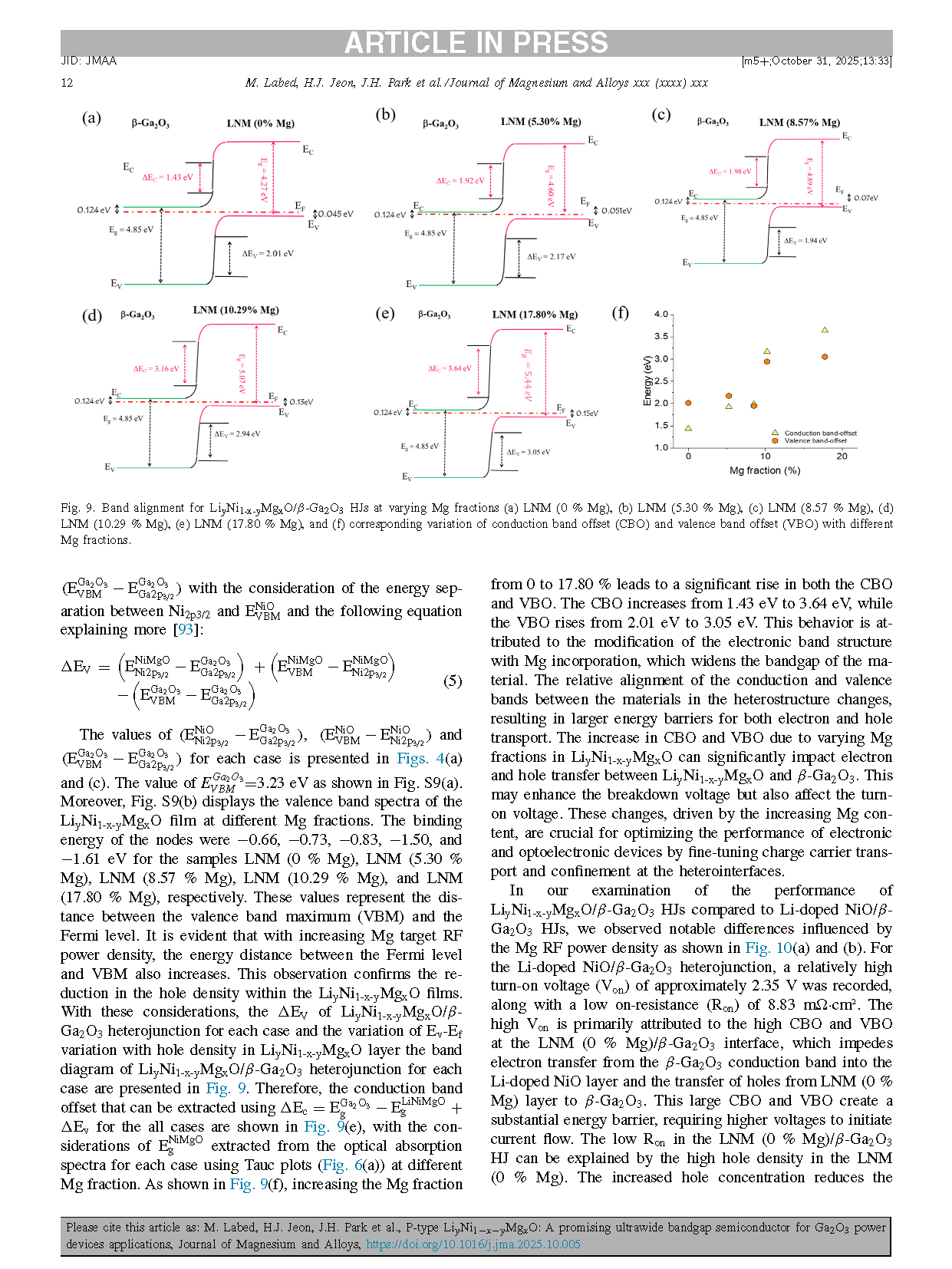
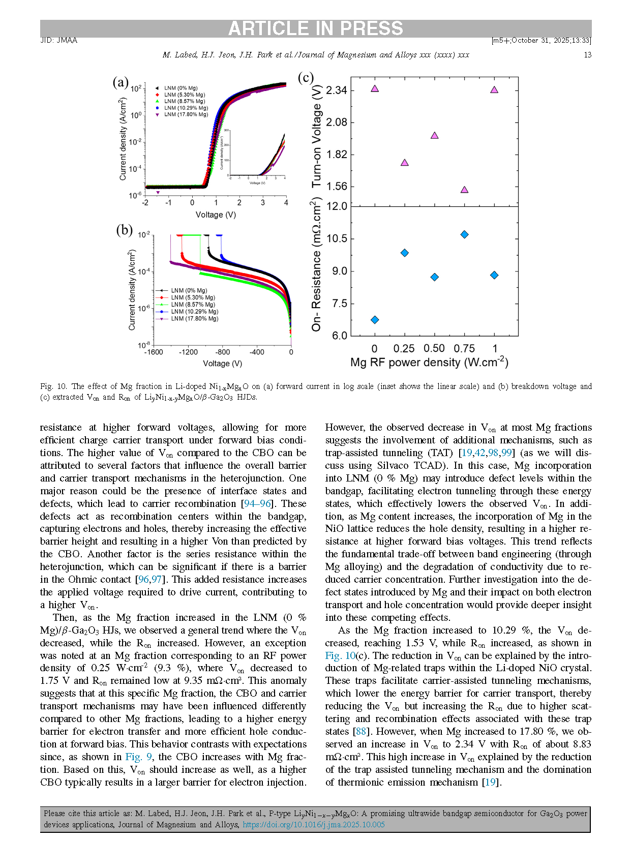
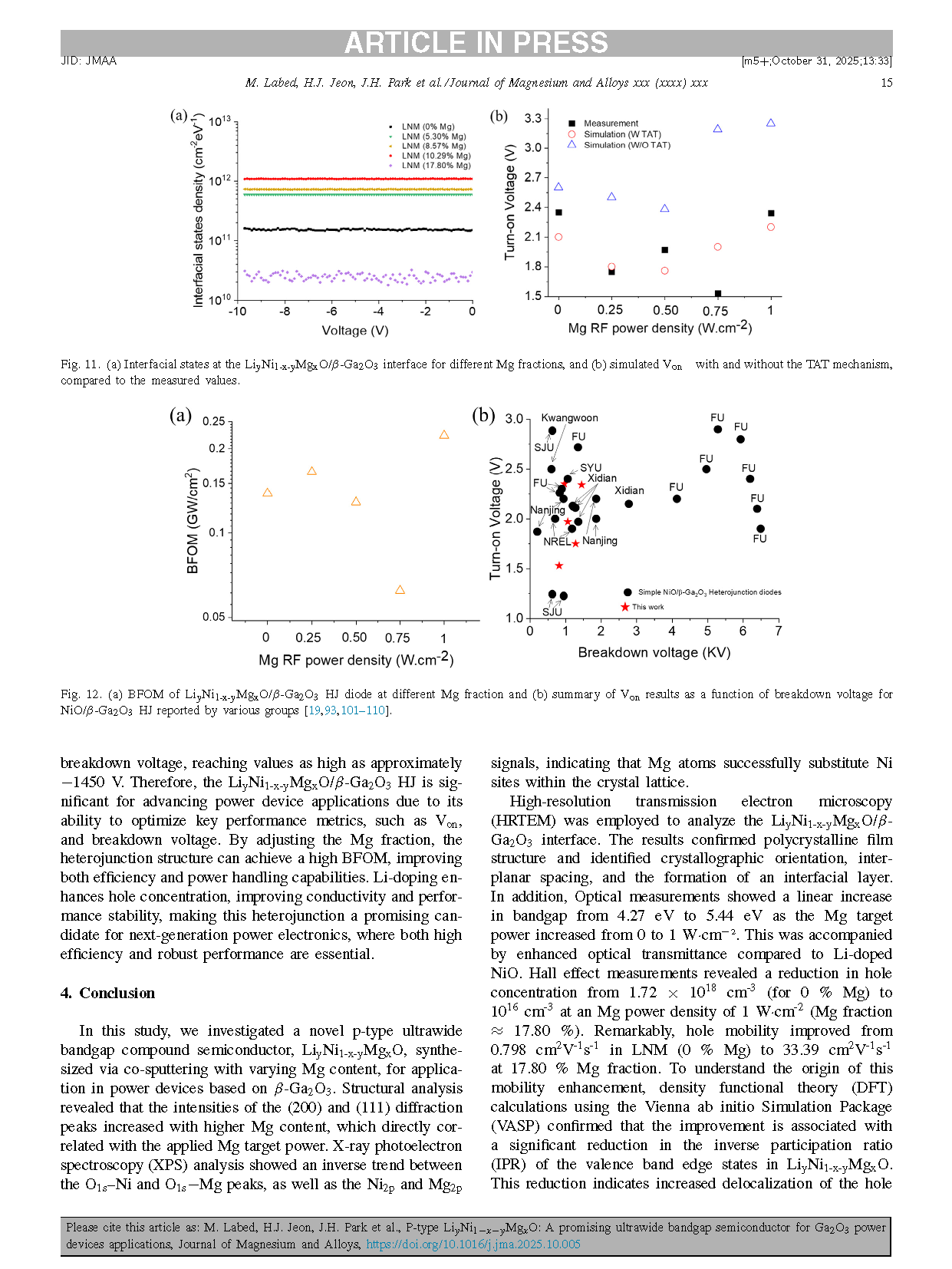
XPS-based band alignment with β-Ga2O3 showed that the conduction band offset increased with Mg content, affecting both turn-on voltage (Von) and breakdown voltage (BV). At 5.30% Mg, the device exhibited BV = −1280 V, Von = 1.73 V, and on-resistance = 9.86 m·cm². At 17.80% Mg, BV increased to −1450 V, Von slightly rose to 2.34 V, and on-resistance decreased to 8.83 m·cm². Despite the larger conduction band offset, Silvaco TCAD simulations confirmed that the reduction in Von at higher Mg fractions results from trap-assisted tunneling via Mg-induced energy levels.
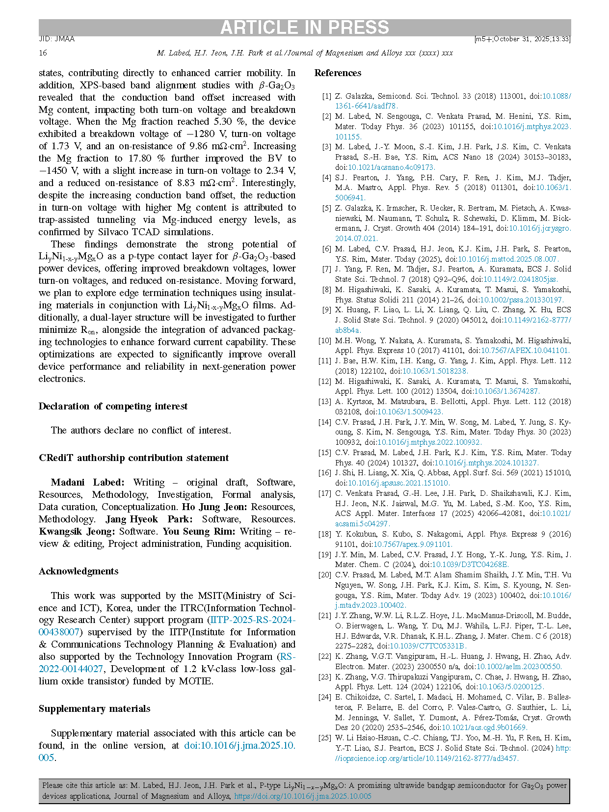
These results demonstrate that LiyNi1-x-yMgxO is a promising p-type contact layer for β-Ga2O3-based power devices, offering higher breakdown voltage, lower turn-on voltage, and reduced on-resistance. Future work will explore edge termination techniques with insulating layers, dual-layer structures to further minimize Ron, and integration of advanced packaging technologies to enhance forward current capability, aiming to improve overall device performance and reliability in next-generation power electronics.
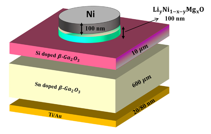
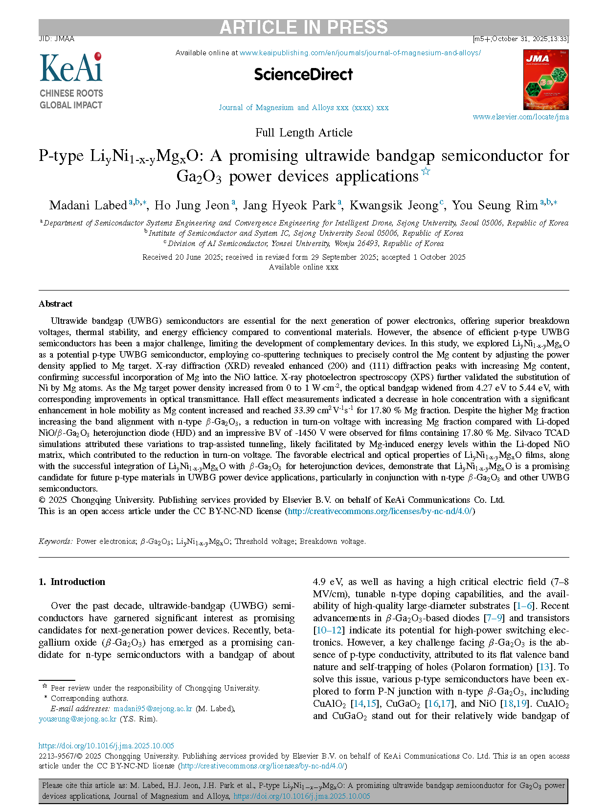
Fig. 1. Schematic diagram of the fabricated device.
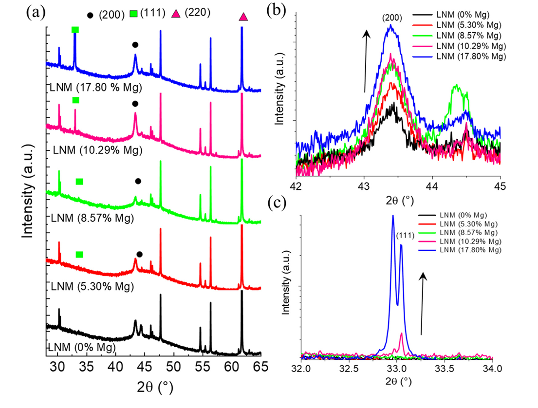
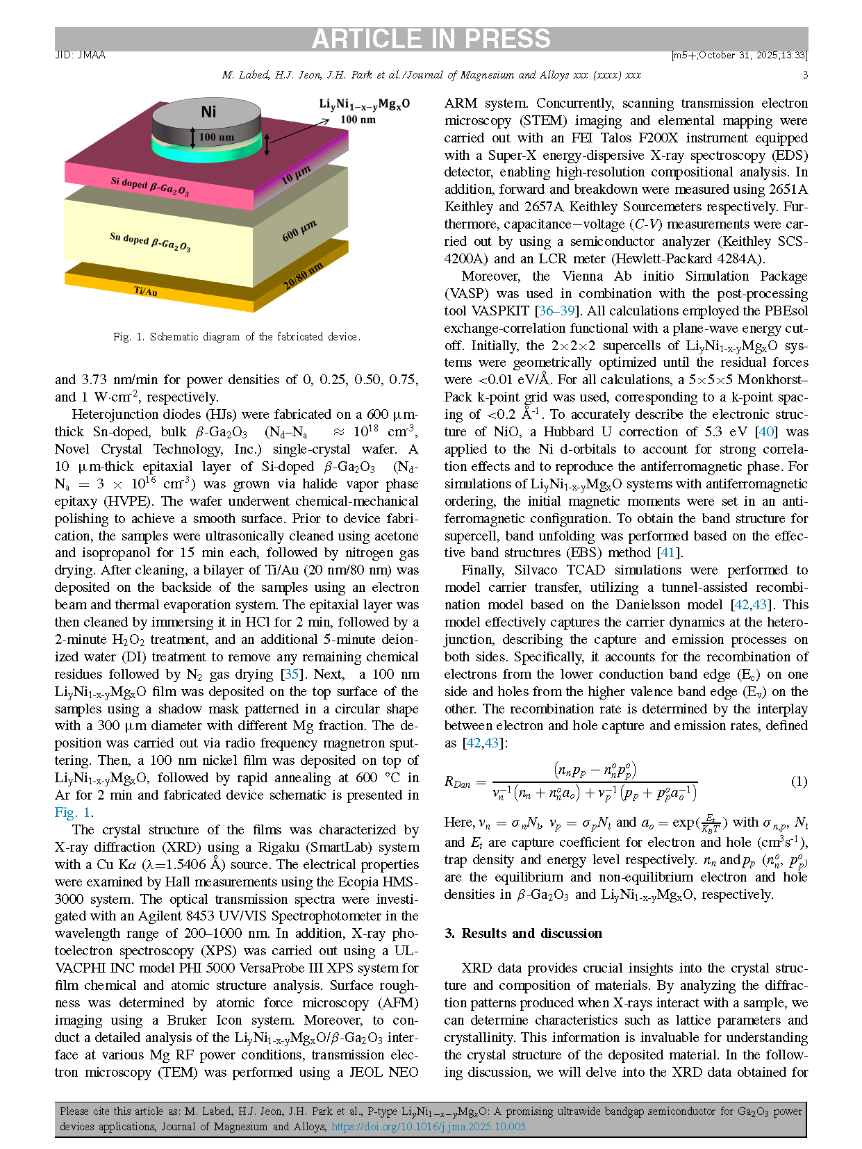
Fig. 2. (a) XRD patterns of p-type LiyNi1-x-yMgxO thin films, (b) (200) and (c) (111) crystallographic orientations under different Mg target RF power density.
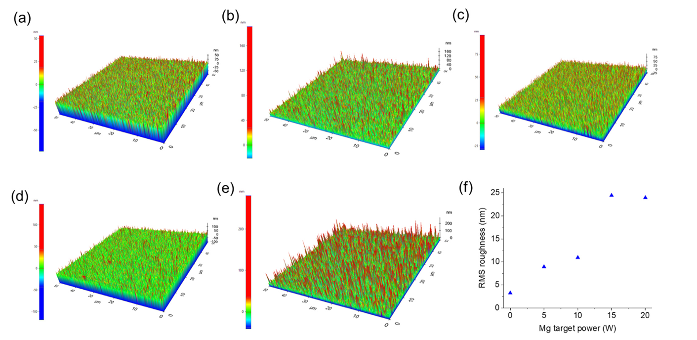
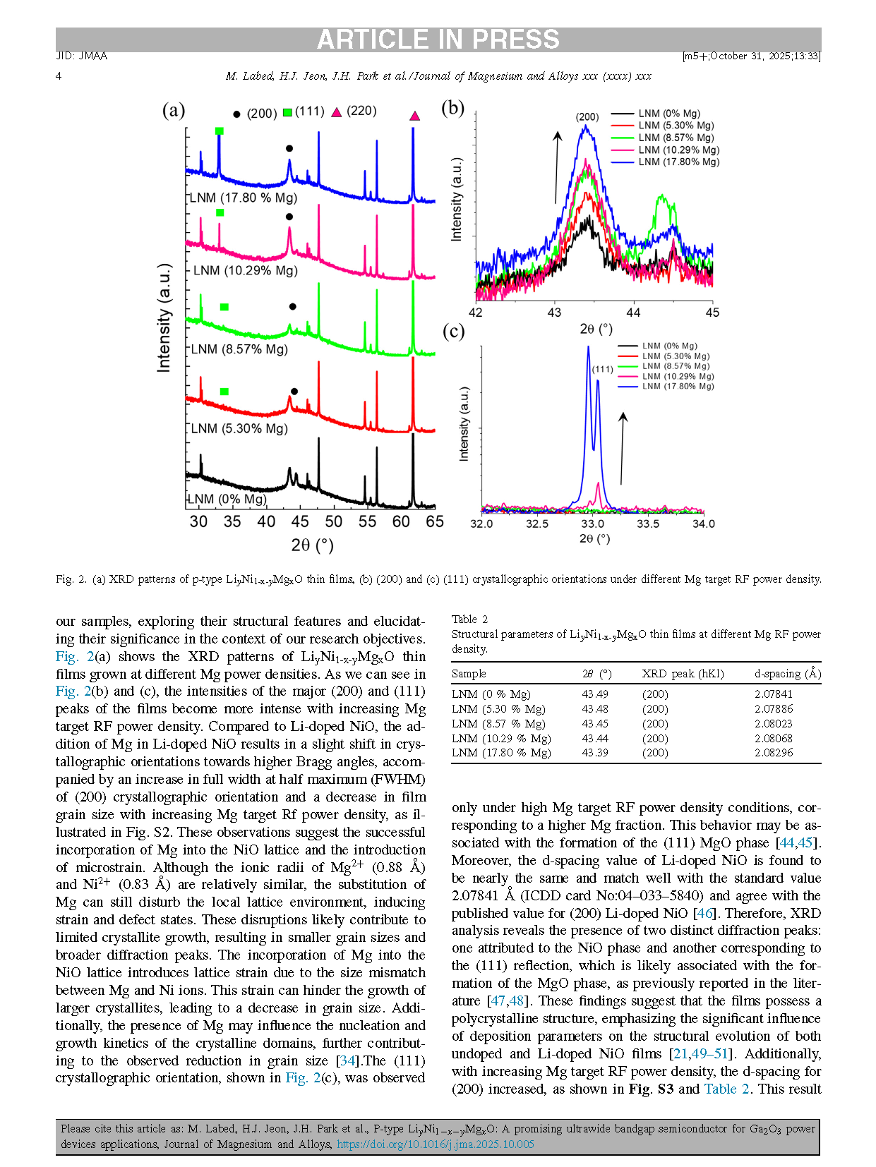
Fig. 3. AFM images of (a) LNM (0 % Mg) (b) LNM (5.30 % Mg), (c) LNM (8.57 % Mg), (d) LNM (10.29 % Mg), (e) LNM (17.80 % Mg) and (f) the extracted RMS roughness.

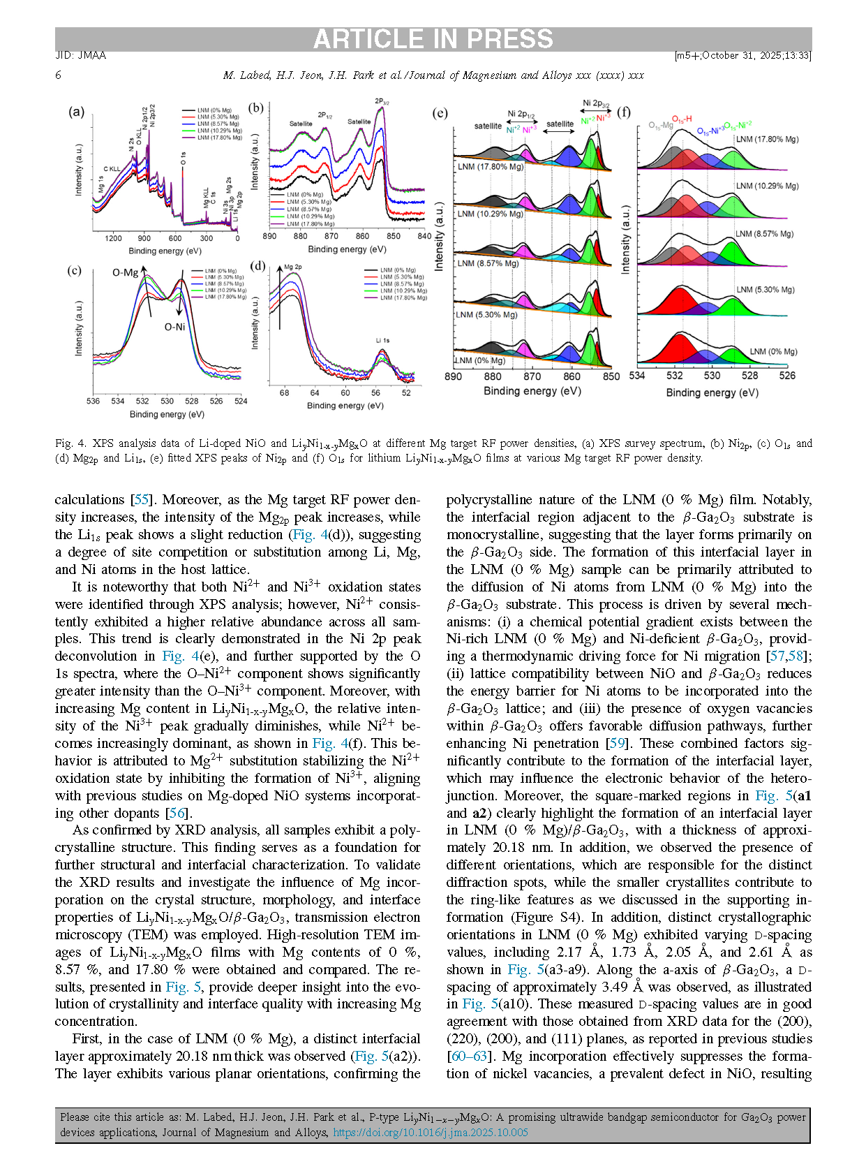
Fig. 4. XPS analysis data of Li-doped NiO and LiyNi1-x-yMgxO at different Mg target RF power densities, (a) XPS survey spectrum, (b) Ni2p , (c) O1s and (d) Mg2p and Li1s , (e) fitted XPS peaks of Ni2p and (f) O1s for lithium LiyNi1-x-yMgx O films at various Mg target RF power density.
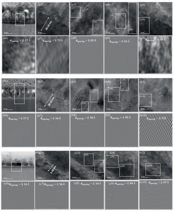
Fig. 5. TEM images illustrating the LiyNi1-x-yMgxO/ β-Ga2O3 heterojunction interfaces for varying Mg fraction: (a) LNM (0 % Mg): (a1) and (a2) show the formation of the interfacial layer; (a3)–(a9) present inverse fast Fourier transform (IFFT) images highlighting different crystallographic orientations; (a10) displays the corresponding interfacial layer. (b) LNM (8.57 % Mg): (b1) and (b2) illustrate the interfacial region; (b3)–(b9) present IFFT images for various orientations; (b10) shows the associated interfacial layer. (c) LNM (17.80 % Mg): (c1) and (c2) show the interface region; (c3)–(c9) provide IFFT images for different orientations; (c10) highlights the interfacial layer structure.
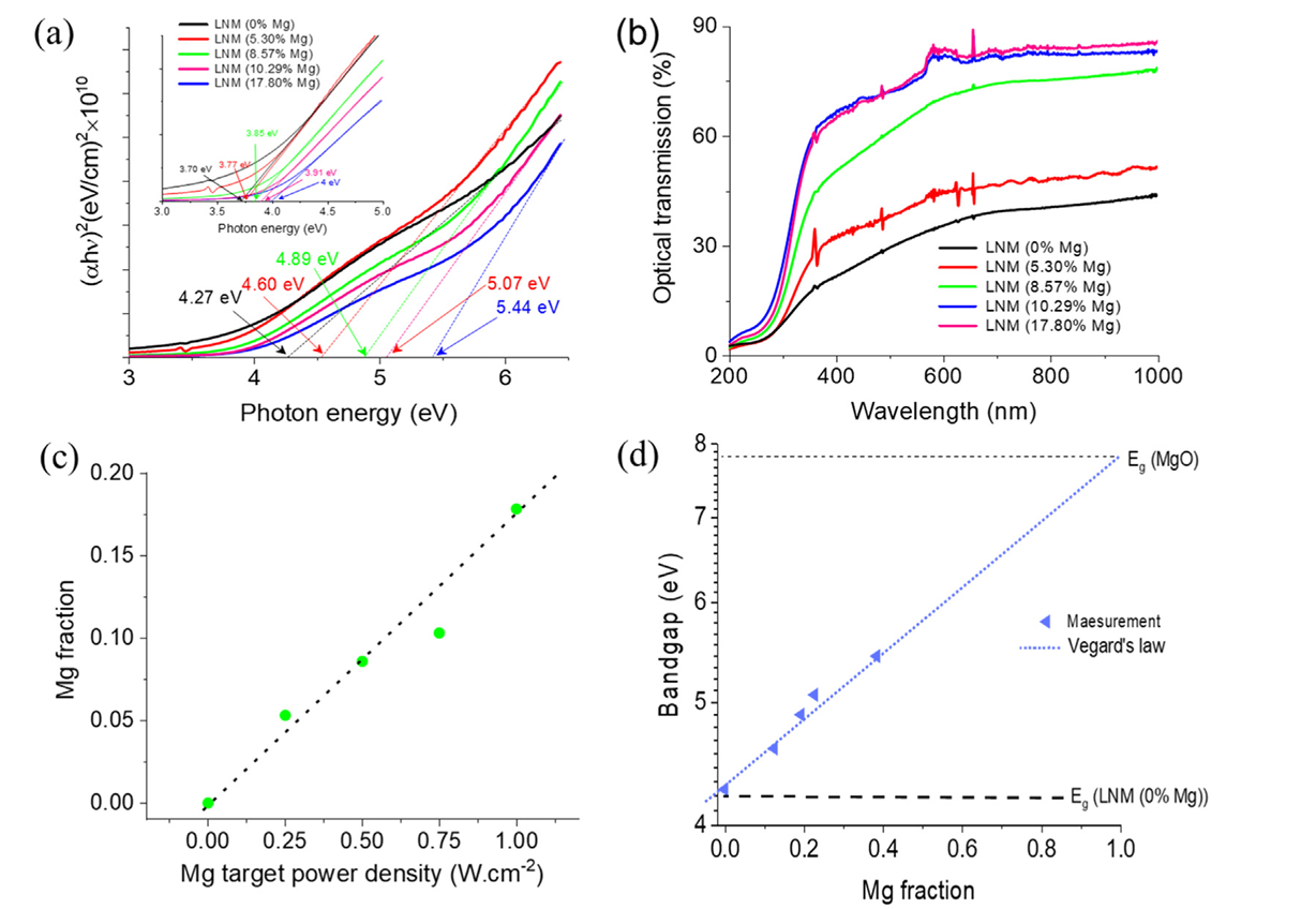
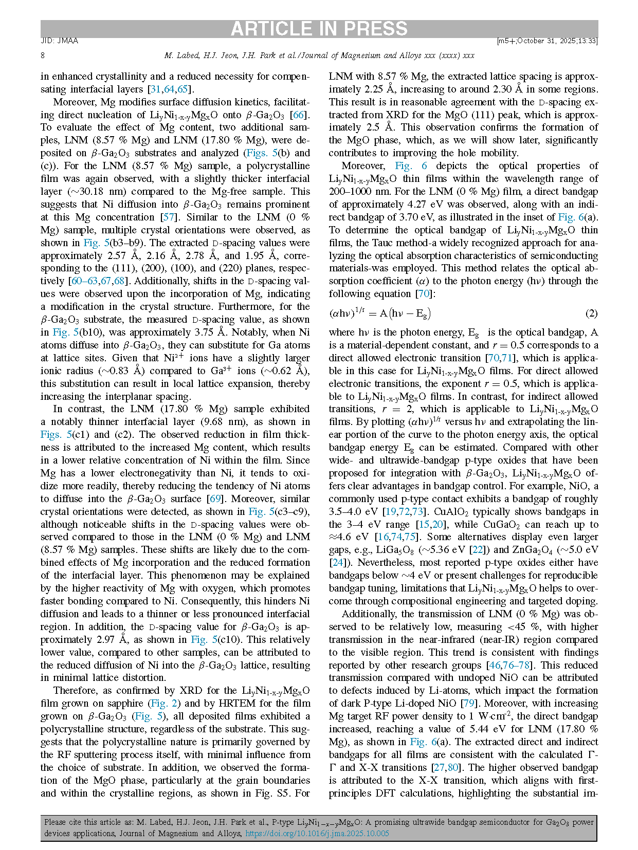
Fig. 6. (a) LiyNi1-x-yMgxO optical absorption showing the direct bandgap and the inset showing the indirect bandgap, (b) optical transmission, (c) extracted Mg faction dependent Mg target RF power density and (d) LiyNi1-x-yMgxO direct bandgap dependent Mg fraction.
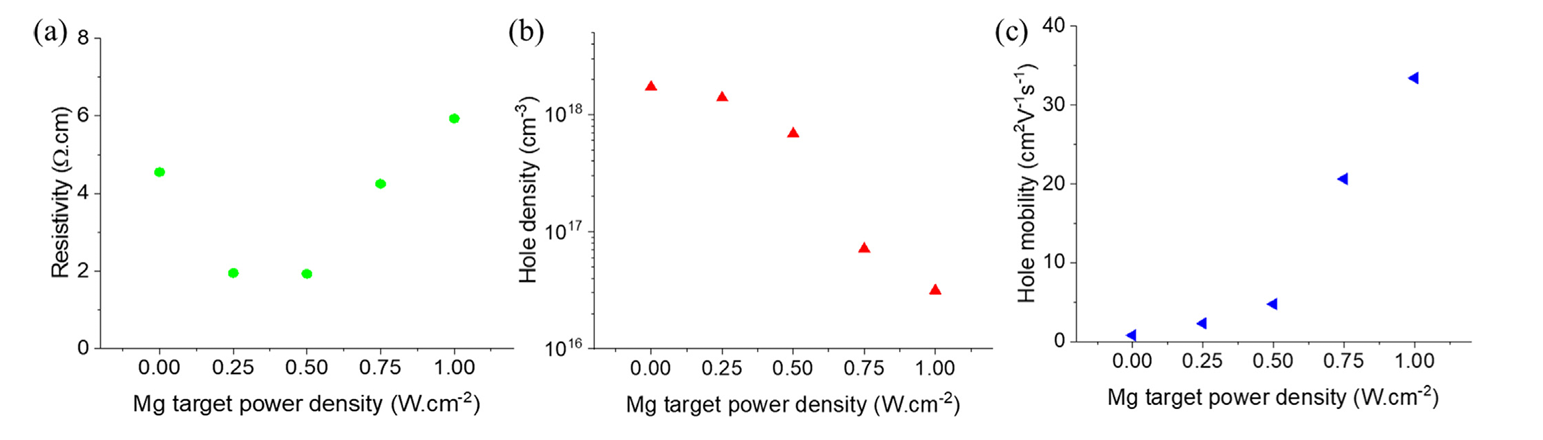
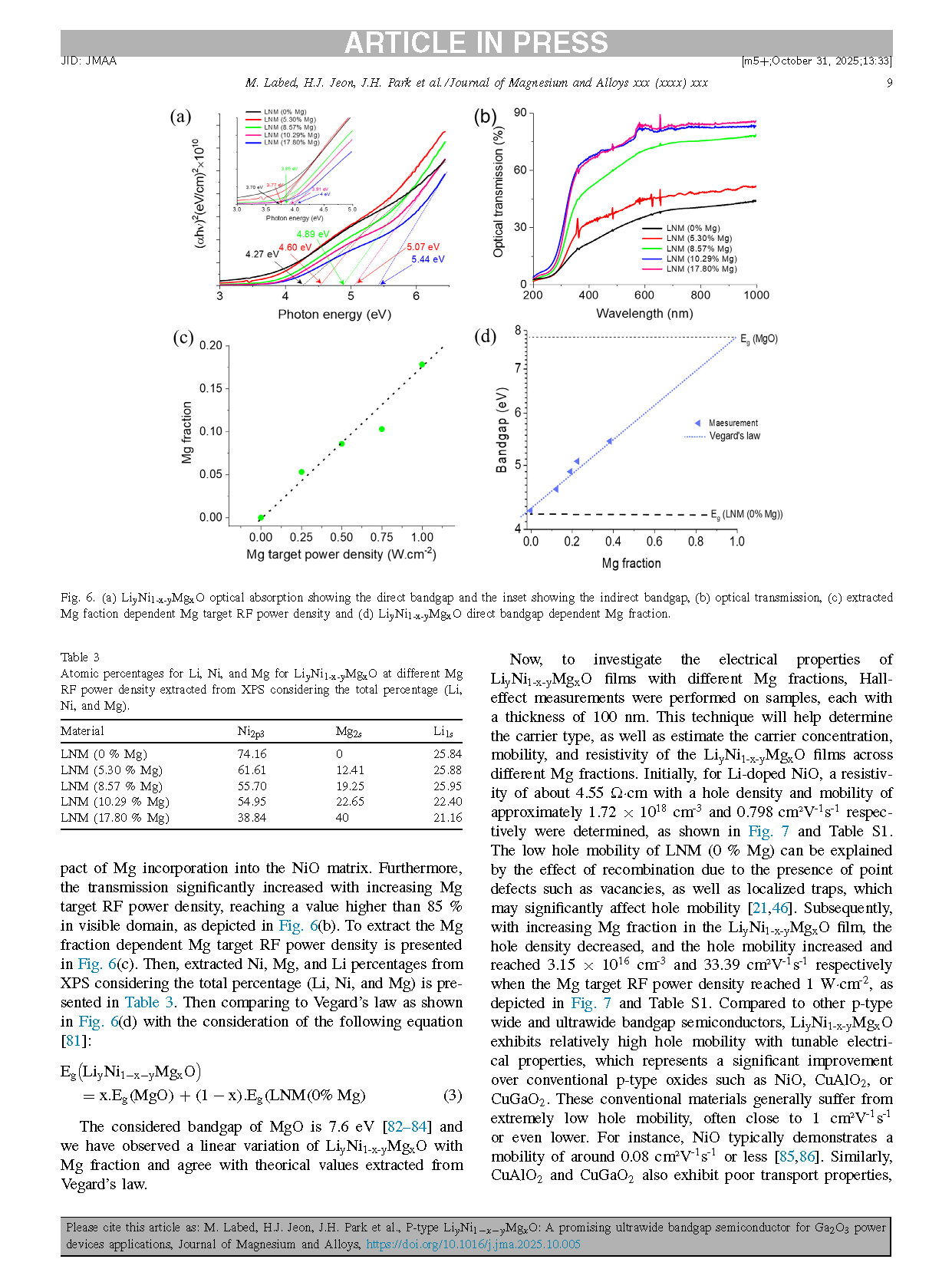
Fig. 7. Room temperature measurements of (a) resistivity, (b) hole density, and (c) hole mobility of LiyNi1-x-yMgxO at different Mg target RF power density.

Fig. 8. Density of states (DOS) and inverse participation ratio (IPR) of LiyNi1-x-yMgxO at various Mg doping concentrations: (a) 0 %, (b) 6.25 %, (c) 12.5 %, (d) 18.75 %, (e) 25 %, and (f) 31.25 %. The black solid lines represent the total DOS, red solid lines denote the Li-projected DOS, and blue bars indicate the IPR of Li. Positive and negative values correspond to spin-up and spin-down states, respectively. A clear reduction in both the IPR and the DOS near the valence band edge is observed with increasing Mg concentration.
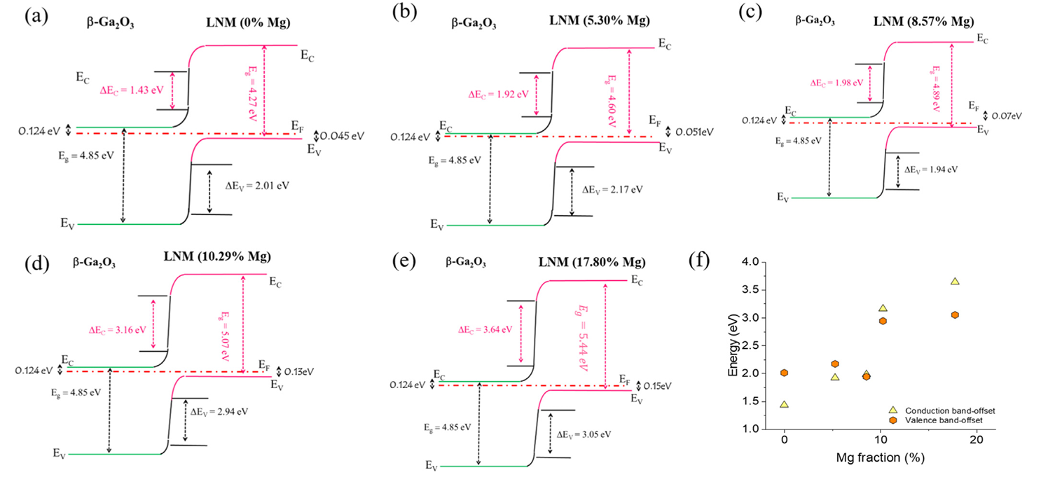
Fig. 9. Band alignment for LiyNi1-x-yMgxO / β-Ga2O3 HJs at varying Mg fractions (a) LNM (0 % Mg), (b) LNM (5.30 % Mg), (c) LNM (8.57 % Mg), (d) LNM (10.29 % Mg), (e) LNM (17.80 % Mg), and (f) corresponding variation of conduction band offset (CBO) and valence band offset (VBO) with different Mg fractions.
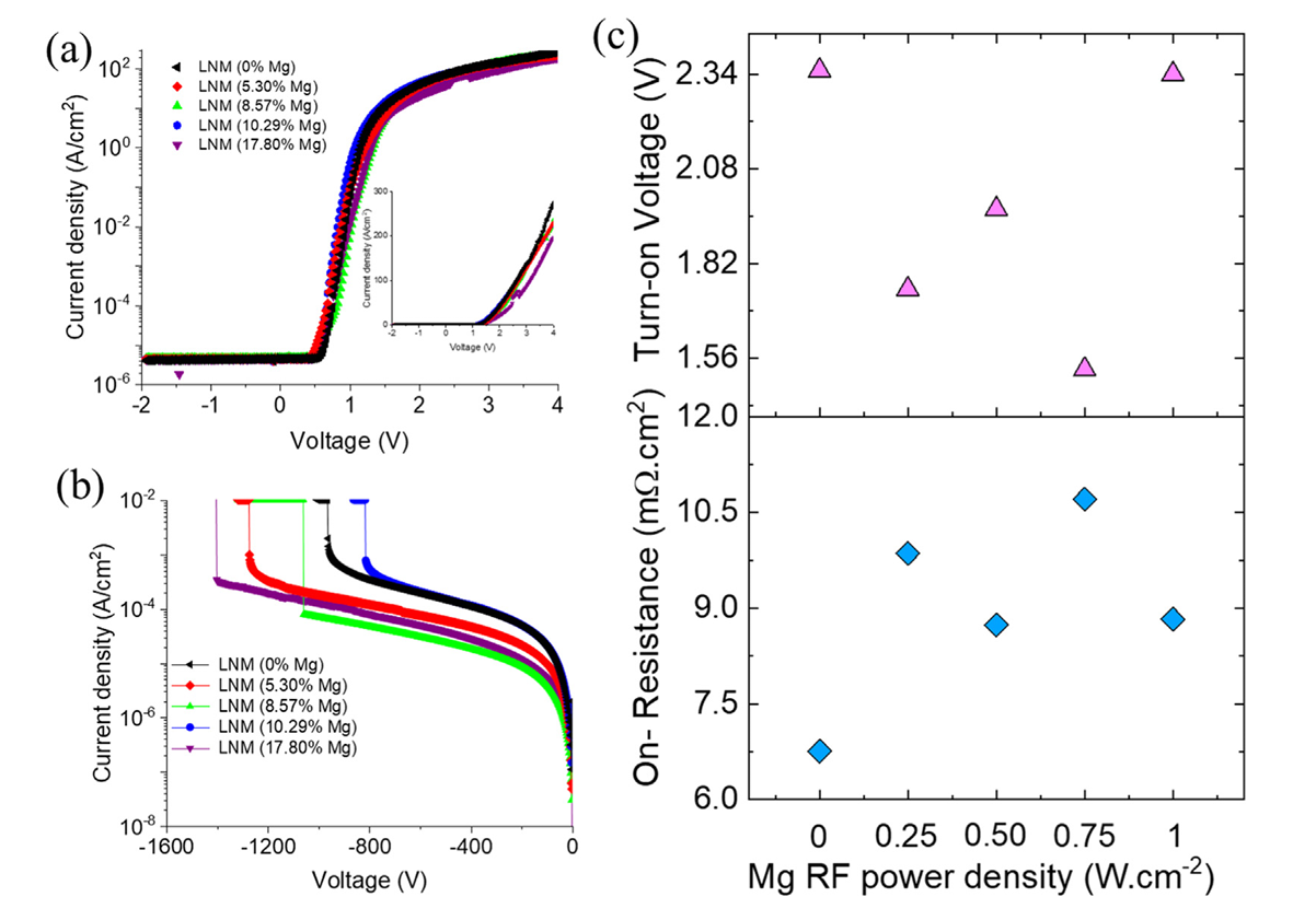
Fig. 10. The effect of Mg fraction in Li-doped Ni1-xMgxO on (a) forward current in log scale (inset shows the linear scale) and (b) breakdown voltage and (c) extracted Von and Ron of LiyNi1-x-yMgxO/ β-Ga2O3 HJDs.
DOI:
doi.org/10.1016/j.jma.2025.10.005