Paper Sharing
【Member Papers】2 kV β-Ga₂O₃ Schottky diode with HfO₂/SiO₂ dual-layer field plate and mesa termination
日期:2025-11-20阅读:485
Researchers from the Xidian University have published a dissertation titled "2 kV β-Ga2O3 Schottky diode with HfO2/SiO2 dual-layer field plate and mesa termination " in Applied Physics Letters.
Project Support
This work was supported by the National Natural Science Foundation of China (Grant Nos. 62304170 and 62374122), the Guangdong Basic and Applied Basic Research Foundation (Nos. 2023B1515040024 and 2022A1515111137), the Fundamental Research Funds for the Central Universities (No. ZYTS25302), and the Xidian University Specially Funded Project for Interdisciplinary Exploration (No. TZJH2024057).
Background
β-Ga₂O₃, as an ultra-wide bandgap semiconductor material (E₉ ≈ 4.9 eV), possesses an extremely high critical breakdown electric field (≈8 MV/cm) and a considerable electron mobility (theoretical value 250 cm²/V·s), showing great potential in high-voltage and high-power electronic devices. Compared with SiC and GaN, β-Ga₂O₃ single-crystal substrates can be fabricated at low cost and high quality using methods such as HVPE, making industrial-scale production feasible.
In the study of vertical β-Ga₂O₃ Schottky barrier diodes (SBDs), various terminal structure optimization strategies have been proposed to enhance breakdown voltage (BV) and power figure of merit (PFOM = BV²/R_on,sp), including ion implantation, field plates, NiOₓ p–n heterojunction terminals, trench structures, and high-permittivity oxide field plates. However, conventional SiO₂ or Si₃N₄ field plates suffer from low dielectric constants and high interface trap densities, making it difficult to effectively alleviate electric field crowding. On the other hand, single high-k materials (e.g., HfO₂, BaTiO₃) can improve interface states, but their limited dielectric breakdown strength constrains overall performance improvement.
Abstract
In this Letter, a vertical β-Ga2O3 Schottky barrier diode (SBD) featuring a composite termination structure with dual-layer field plate and self-aligned etched mesa (DFPM-SBD) is proposed. By combining a high-k HfO2 and SiO2 bilayer dielectric as the field plate termination, the interfacial trap state can be effectively reduced and the electric field crowding effect can be effectively alleviated in β-Ga2O3 SBD. Moreover, the self-aligned etching process is implemented using high-hardness Pt metal as the etching mask, effectively eliminating alignment deviation, thereby contributing to a high breakdown voltage (BV). The experimental result demonstrates that the DFPM-SBD achieves a low Von of 0.68 V (@1 A/cm2), an ideality factor of 1.07, a Schottky barrier height (qΦb) of 1.25 eV, a low specific on-resistance of 3.85 mΩ cm2 along with a high BV of 2050 V, yielding a Baliga's power figure of merit of 1.1 GW/cm2. Furthermore, the interface trap density (Dit) of β-Ga2O3 SBDs is measured, and it is found that the HfO2 layer can effectively reduce the interfacial Dit from 3.25 × 10¹² to 4.76 × 1011 cm−2eV−1, showing an 85% reduction, with a trap energy level located at ET in a range of 0.21–0.25 eV below the EC and the time constant ranging from 4.46 to 8.36 × 10⁻⁵ ms. Therefore, this work provides important guidance of β-Ga2O3 SBD for high-power applications, pushing the development of ultra-wide gap semiconductors greatly.
Conclusion
In summary, an efficient edge termination with deep etching mesa and HfO2/SiO2 dual field plate is achieved in vertical β-Ga2O3 SBD, with a high PFOM of 1.1GW/cm2. The key implementation of self-aligned etching mesa formation combined with a dielectric field plate significantly alleviates the electric field crowding effect, showing an affordable electric field peak of 17MV/cm on the anode edge in TCAD simulation and realizing a critical electric field value of 15% below the theoretical breakdown limit of β-Ga2O3. Furthermore, it is verified by the conductance-frequency analysis that the HfO2 passivation layer can reduce the interfacial trap state from 1.16 × 10¹² to 4.76 × 10¹¹ cm⁻²·eV⁻¹, which is mainly induced by the etching process for isolation and presenting as shallow-level traps. Therefore, this work demonstrates that high-k dielectric shows exceptional promise for enhancing β-Ga2O3 SBD performance, and the proposed composite termination structure with dual field plate and self-aligned etched mesa for vertical β-Ga2O3 SBD provides critical design insights for next-generation high-power, high-voltage devices.
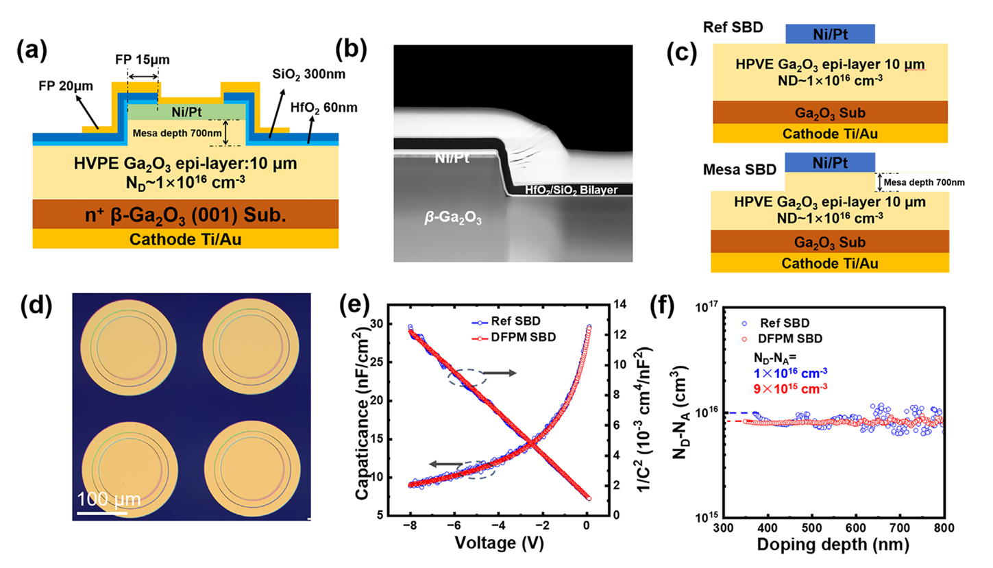
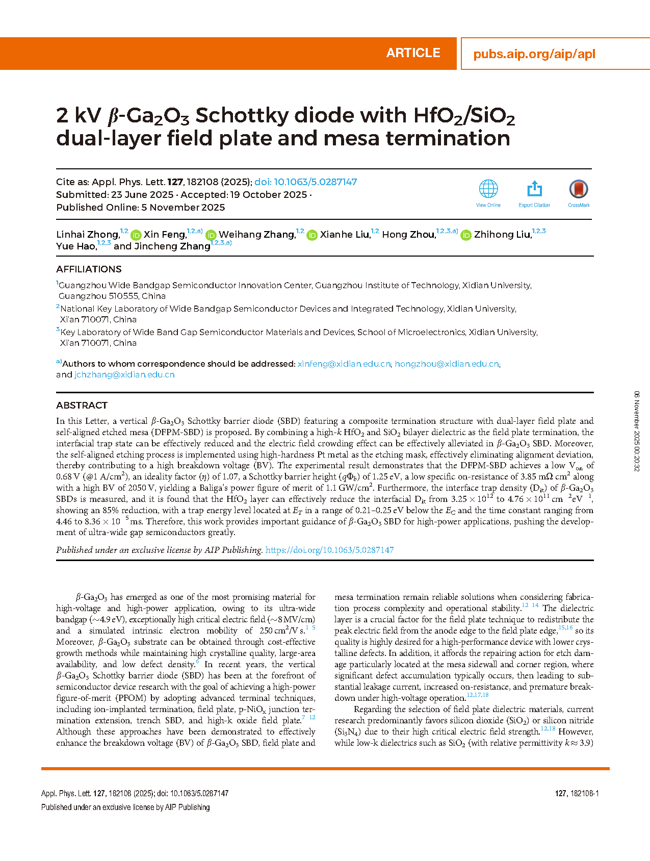
FIG. 1. (a) Cross-sectional schematic of the DFPM-SBD. (b) The STEM image of the DFPM-SBD. (c) Cross-sectional schematic of the Ref-SBD and Mesa-SBD. (d) The optical microscope image of the DFPM-SBD. (e) Normalized C–V and 1/C2–V curves of the Ref-SBD and DFPM-SBD. (f) Extracted ND-NA of the Ref-SBD and DFPM-SBD.
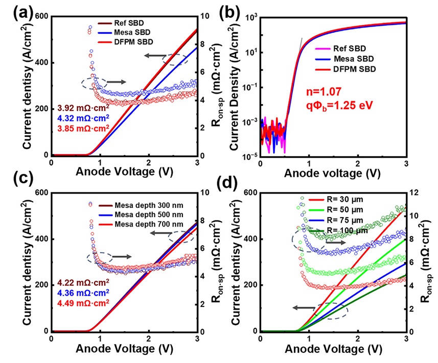
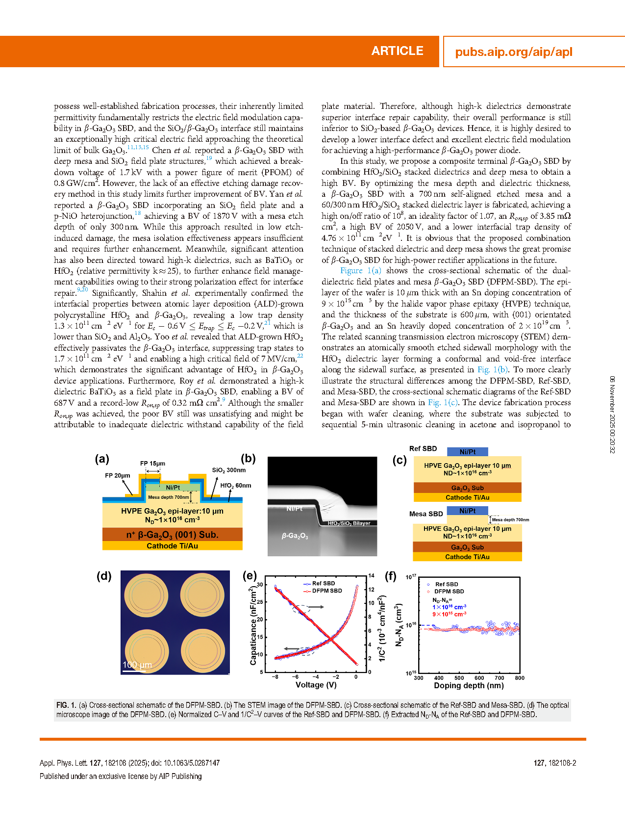
FIG. 2. The normalized DC (a) linear-scale (b) log-scale forward IF–VF and differential Ron,sp–VF measurement result of the Ref-SBD, Mesa-SBD, and DFPM-SBD. (c) The nor malized DC linear-scale IF–VF and differential Ron,sp–VF characteristics of the Mesa-SBD with mesa depths of 300, 500, and 700nm. (d) The normalized DC linear-scale IF–VF and differential Ron,sp–VF characteristics of the DFPM-SBD with different anode areas.
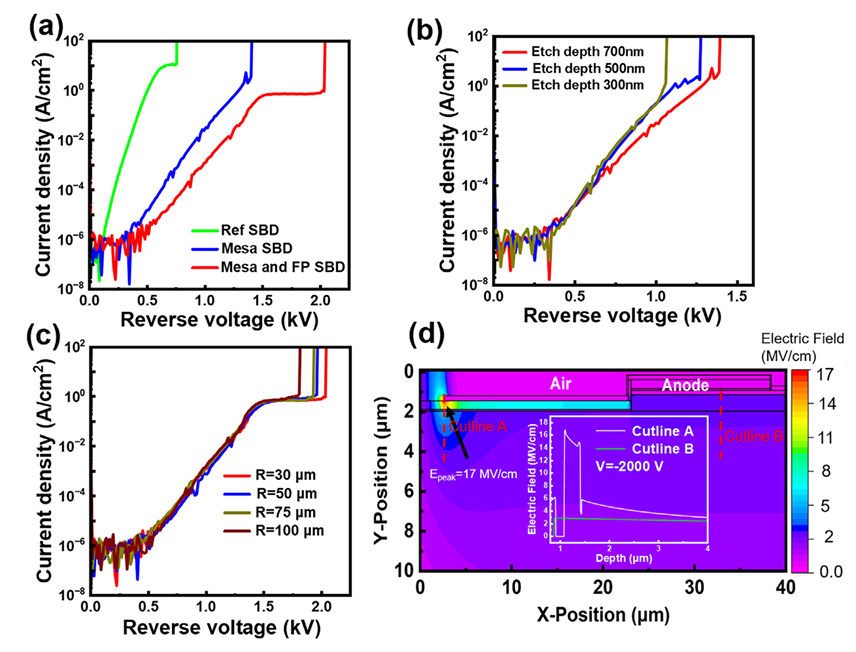
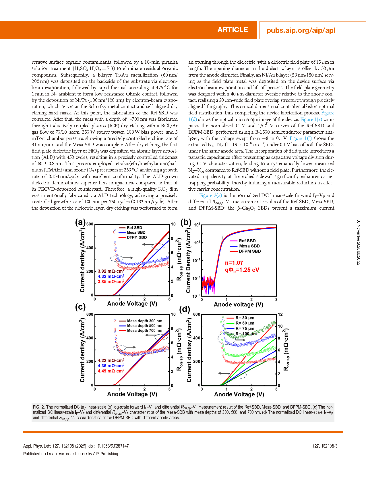
FIG. 3. (a) Reverse characteristics of the Ref-SBD, Mesa-SBD, and DFPM-SBD with an anode diameter of 60lm. (b) Reverse characteristics of the Mesa-SBD with different mesa depths. (c) Reverse characteris tics of the DFPM-SBD with different anode areas. (d) The simulated critical electric field distribution of the DFPM device under a reverse bias of 2000V.
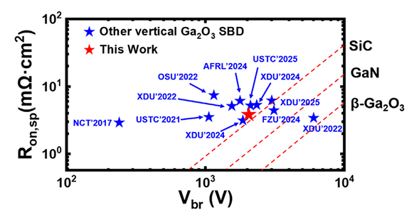
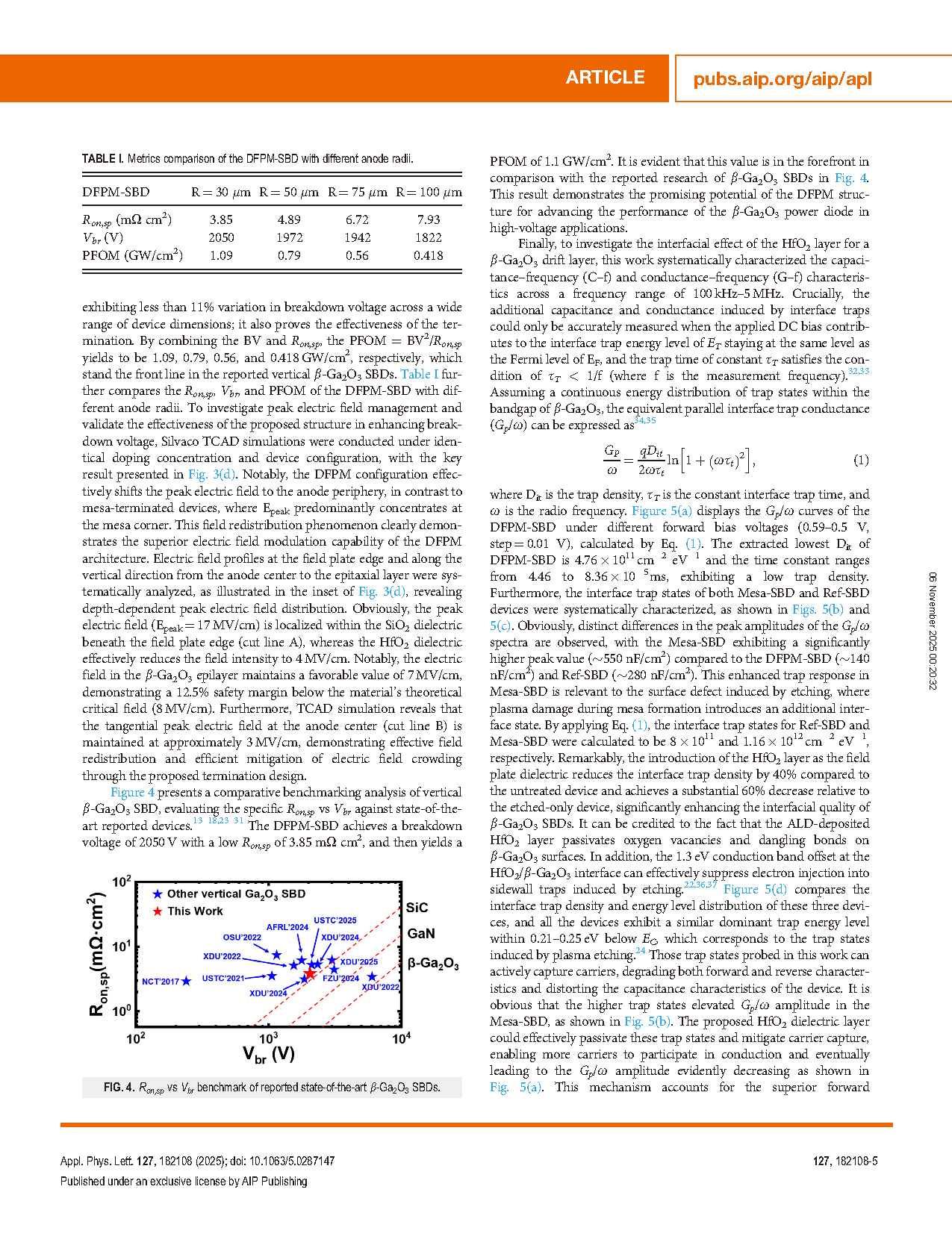
FIG. 4. Ron,sp vs Vbr benchmark of reported state-of-the-art β-Ga2O3 SBDs.
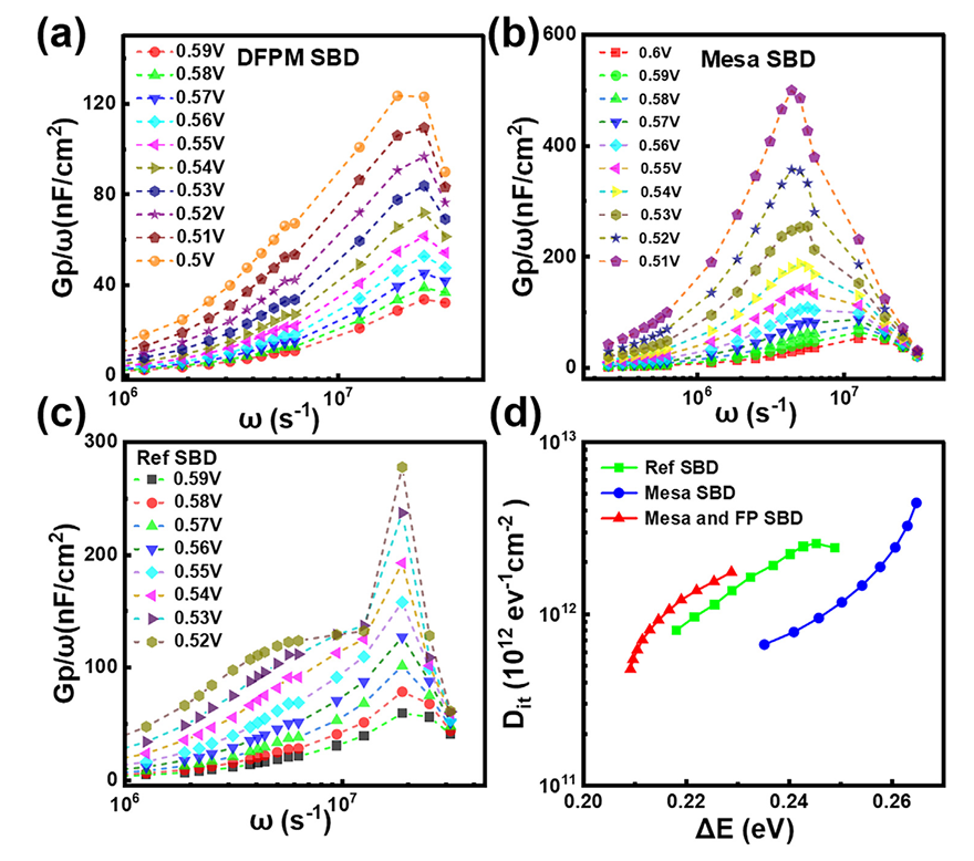
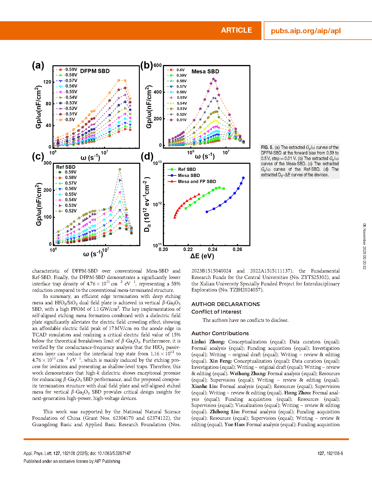
FIG. 5. (a) The extracted Gp/ω curves of the DFPM-SBD at the forward bias from 0.59 to 0.5 V, step=0.01 V. (b) The extracted Gp/ω curves of the Mesa-SBD. (c) The extracted Gp/ω curves of the Ref-SBD. (d) The extracted Dit–△E curves of the devices.
DOI:
doi.org/10.1063/5.0287147