Paper Sharing
【Domestic Papers】Ga₂O₃ MISM photodiode arrays with an HfO₂ insulator achieving a 20 fA dark current for solar-blind imaging
日期:2025-11-20阅读:476
Researchers from the Beijing University of Posts and Telecommunications have published a dissertation titled "Ga2O3 MISM photodiode arrays with an HfO2 insulator achieving a 20 fA dark current for solar-blind imaging" in Optics Letters.
Project Support
This work is supported by National Natural Science Foundation of China (12474065); State Key Laboratory of Information Photonics and Optical Communications (IPOC2025ZR05); Fundamental Research Funds for the Central Universities (BUPT, 2023ZCJH1); BUPT Excellent Ph.D. Students Foundation (CX20253002).
Background
In recent years, advances in deep ultraviolet (DUV) communication and photodetection have driven increasing demand for high-sensitivity imaging systems. Multi-pixel arrays enhance information capacity, while their solar-blind nature enables background-free detection of faint signals. Although Si-based solar-blind photodetectors offer low cost and mature processing, they suffer from limited penetration of high-energy UV photons, finite responsivity in the solar-blind band, thermal instability, and reliance on external filters. Consequently, wide-bandgap semiconductors such as MgZnO, AlGaN, diamond, and Ga₂O₃ have emerged as alternatives. Among them, Ga₂O₃ stands out due to its ultra-wide bandgap (≥4.8 eV), high breakdown field, and excellent stability, making it highly suitable for DUV detection. Conventional Ga₂O₃ MSM photodetectors, however, suffer from high dark current and noise due to the lack of an effective potential barrier between electrodes, exacerbated by surface states and dislocations. To address these limitations, this work introduces a HfO₂-insulated metal–insulator–semiconductor–metal (MISM) photon-controlled diode, which increases the interfacial barrier to suppress dark current and noise while enabling high responsivity under UV illumination, offering a promising platform for high-performance DUV imaging.
Abstract
Traditional Ga2O3 metal–semiconductor–metal (MSM) photodetectors suffer from high dark current, limiting their sensitivity for deep ultraviolet (DUV) imaging. This Letter reports a novel, to the best of our knowledge, metal–insulator–semiconductor–metal (MISM) photon-controlled diode with an ultrathin HfO2 insulator. The device achieves an ultralow dark current of ~20 fA at 5 V, representing a two-order-of-magnitude reduction compared to conventional MSM counterparts. The MISM structure exhibits exceptional performance metrics: responsivity of 2188 A/W, noise equivalent power of 1.06 × 10⁻¹⁶ W/Hz1/2, and over 300-fold photo-to-dark current ratio enhancement. The engineered HfO2 layer serves as a wide-bandgap energy barrier, suppressing electron leakage and passivating surface traps to enhance carrier collection efficiency. A 16 × 16 focal plane array demonstrates superior image contrast and spatial resolution under faint DUV illumination (100 nW/cm2). This MISM architecture offers a scalable approach for next-generation high-sensitivity DUV imaging systems.
Conclusion
In summary, we have demonstrated a high-performance Ga2O3-based MISMPCDincorporatinganultrathinHfO2 insulating layer that achieves ultralow dark current ( 20 fA at 5 V)and superior responsivity (2188 A/W). The HfO2 layer plays a dual role—suppressing carrier injection via its high energy barrier while passivating surface states to enhance photocarrier collection. The fabricated 16 × 16 imaging array exhibits exceptional weak-light sensitivity under 100 nW/cm2 illumination, significantly outperforming conventional MSM PDs. These results highlight the MISM architecture as a promising pathway for next-generation high-sensitivity solar-blind imaging systems.
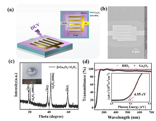
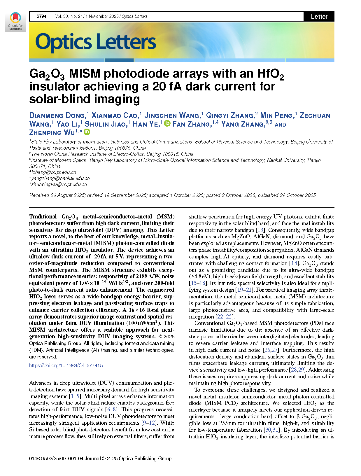
Fig. 1. (a)Schematic of the MISM device structure. (b) SEM im age of the fabricated device. (c) XRD θ–2θ scan of the Ga2O3 film (inset: photo of the 2-inch wafer). (d) Optical transmittance spectrum of β-Ga2O3 (inset: fitted bandgap of 4.95 eV).
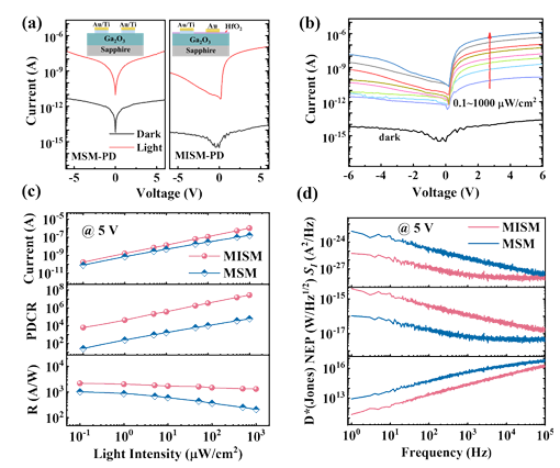
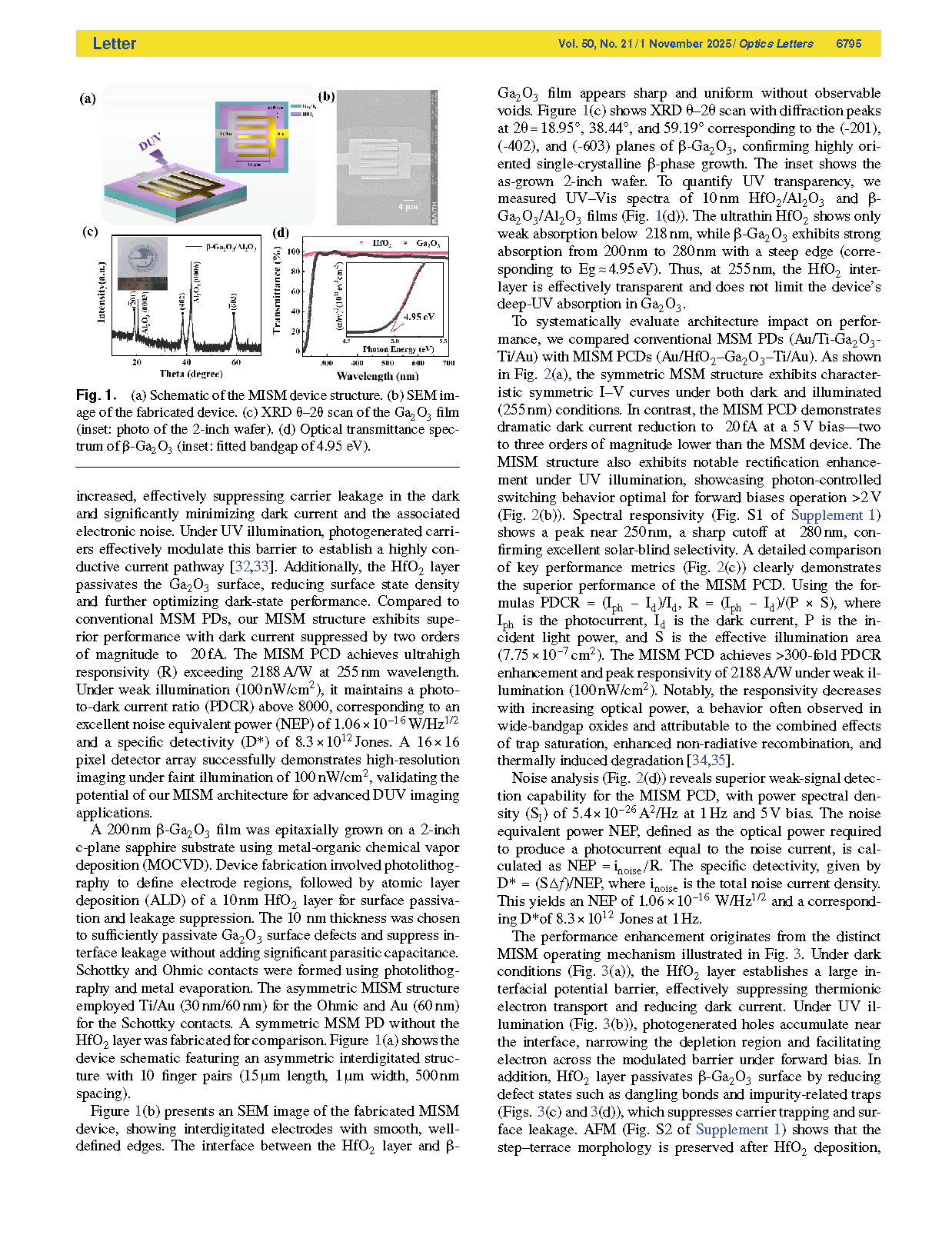
Fig. 2. (a)Comparison of I–V characteristics for both devices under dark and illuminated conditions. (b) I–V curves of the MISM device under varying light intensities. (c) Iph, PDCR, and R functions of light intensity. (d) Comparison of noise current density, NEP, and D* for the two devices.
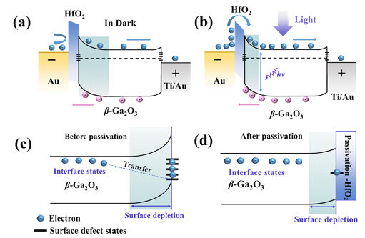
Fig. 3. Energy band structure and carrier transfer in the MISM device. (a) MISM detector in the dark. (b) MSM detector under 255-nm UV light. (c) β-Ga2O3 surface states before passivation. (d) After passivation.
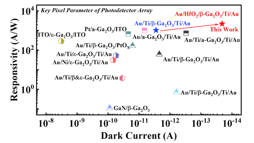
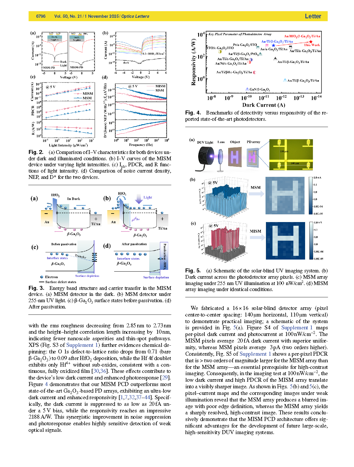
Fig. 4. Benchmarks of detectivity versus responsivity of the reported state-of-the-art photodetectors.
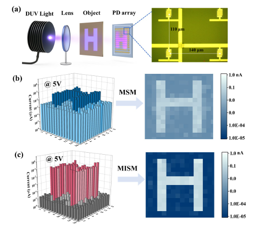
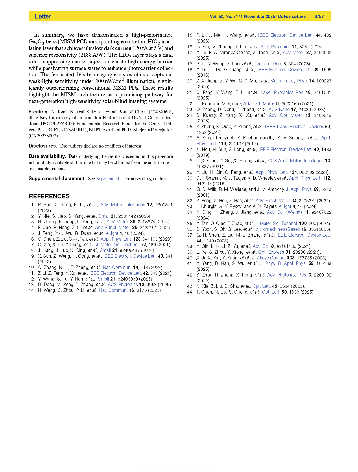
Fig. 5. (a) Schematic of the solar-blind UV imaging system. (b) Dark current across the photodetector array pixels. (c) MSM array imaging under 255 nm UV illumination at 100 nW/cm2. (d) MISM array imaging under identical conditions.
DOI:
doi.org/10.1364/OL.577415