Paper Sharing
【Domestic Papers】Overcoming mobility-off current and mobility-stability trade-offs in solution-processed two-dimensional In₂O₃ transistors via in-situ ultrathin Ga₂O₃ passivation
日期:2025-11-19阅读:487
Team Introduction
Wangying Xu, male, Ph.D., Professor at Jimei University, Fellow of the International Association of Advanced Materials (IAAM Fellow), Fellow of the VEBLEO Society, has long been engaged in research on wide-bandgap oxide thin films and devices. He received his B.E. from Zhejiang University in 2009, M.S. from the Ningbo Institute of Materials Technology and Engineering, Chinese Academy of Sciences in 2012, and Ph.D. from The Chinese University of Hong Kong in 2015. He worked at the Hong Kong Nanotechnology and Advanced Materials R&D Centre from 2015-2016, at Shenzhen University from 2016-2022, and joined Jimei University in 2022. He has received honors including IAAM Fellow (2025), VEBLEO Fellow (2025), Guangdong Pearl River Talents Plan Young Top-notch Talent (2018), and Fujian High-Level Talent (2022). He has published over 100 academic papers, holds 20 patents, with total citations exceeding 3200 and an H-index of 30. He serves as a reviewer for top journals such as Nat. Electron., Nat. Commun., J. Am. Chem. Soc., and Adv. Mater..
Research Background
Two-dimensional ultrathin indium oxide (In₂O₃) transistors are promising candidates for future 3D integrated chip technology, but their development has long been hampered by two core conflicts:
Mobility-Off Current Trade-off: Reducing the channel thickness improves the off-state current but leads to a sharp decline in carrier mobility.
Mobility-Stability Trade-off: The deep Conduction Band Minimum (CBM) of high-mobility In₂O₃ makes it susceptible to interference from oxygen vacancies, H₂O, etc., leading to severe bias-stress instability and unstable electrical properties.
Previous studies often addressed one issue at the expense of the other, unable to resolve these conflicts simultaneously.
Main Content
This study innovatively proposed a strategy of in-situ solution-grown ultrathin Ga₂O₃ passivation, successfully overcoming the aforementioned challenges.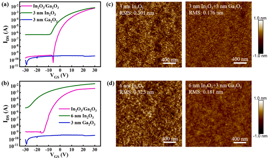
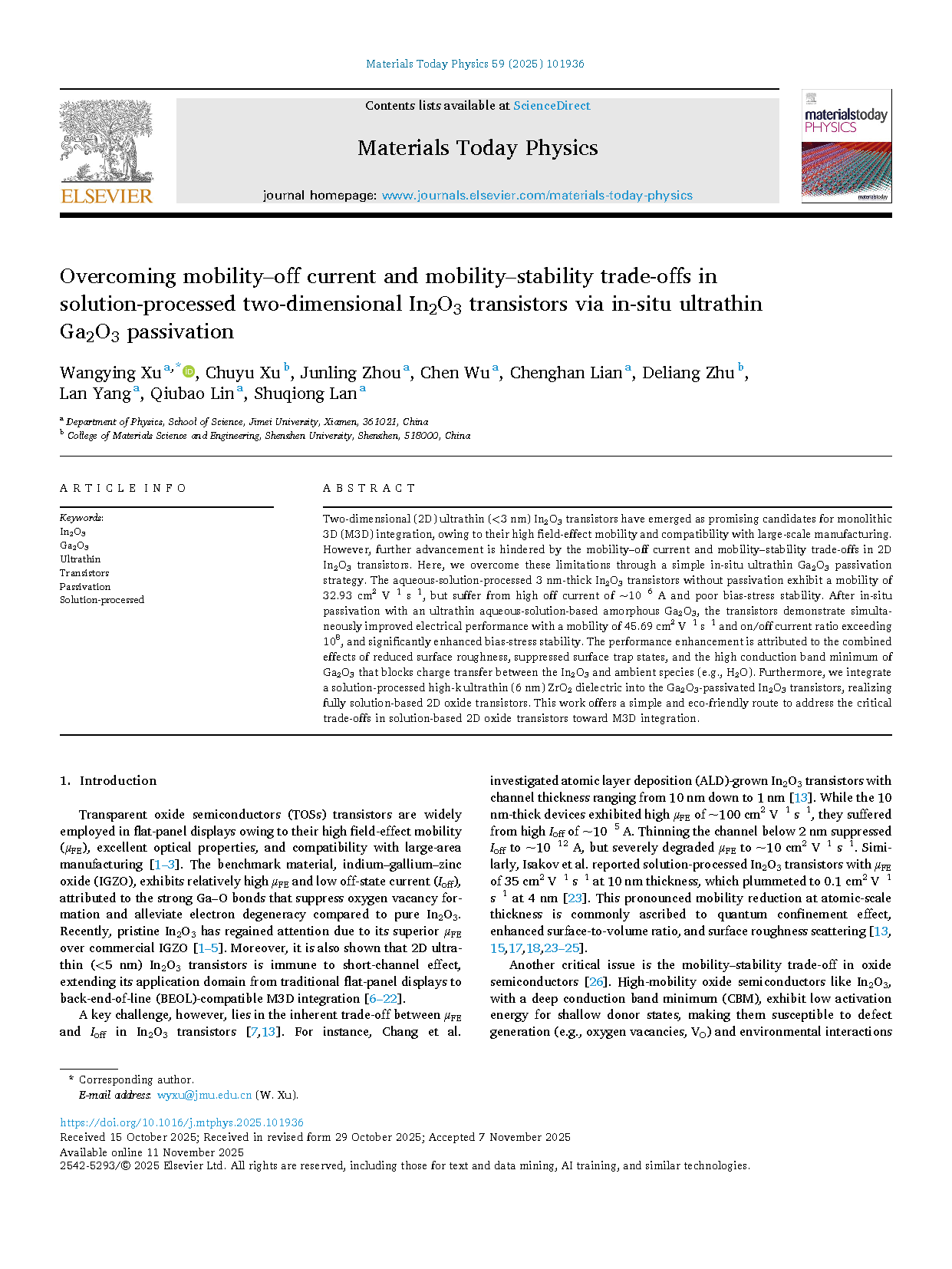
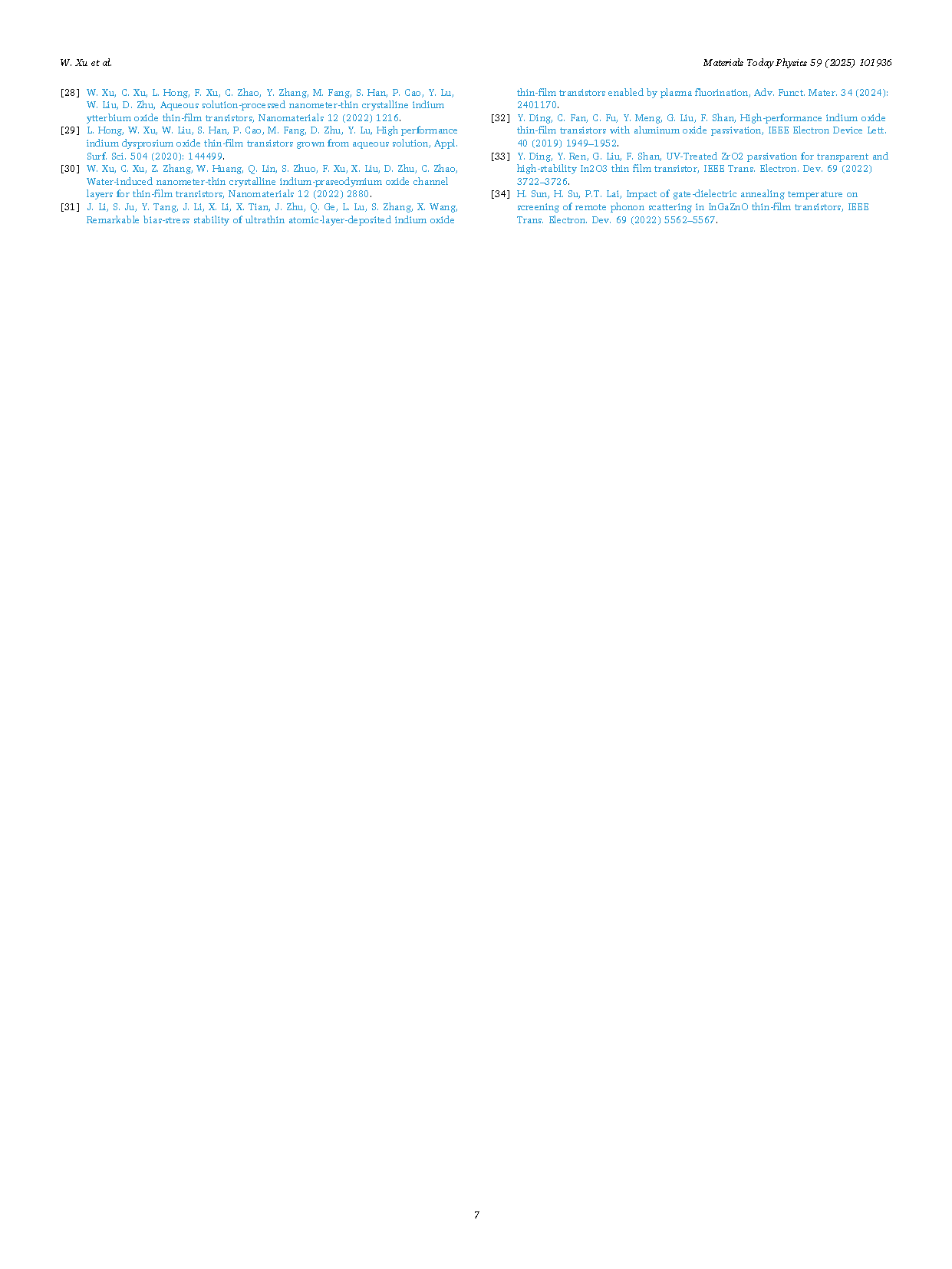
Breakthrough Performance: Unpassivated 3 nm-thick In₂O₃ transistors exhibited a mobility of 32.93 cm² V⁻¹ s⁻¹ but suffered from high off-state current (~10⁻⁶ A) and poor stability. After introducing a 3 nm Ga₂O₃ passivation layer, the mobility significantly increased to 45.69 cm² V⁻¹ s⁻¹, the off-state current was drastically reduced to ~10⁻¹⁰ A, and the on/off current ratio exceeded 10⁸, with all parameters optimized simultaneously.
Significantly Enhanced Stability: Under high-voltage bias-stress tests, the threshold voltage shift of the passivated devices was reduced from over 9 V for unpassivated devices to approximately 1.8 V, improving stability by an order of magnitude.
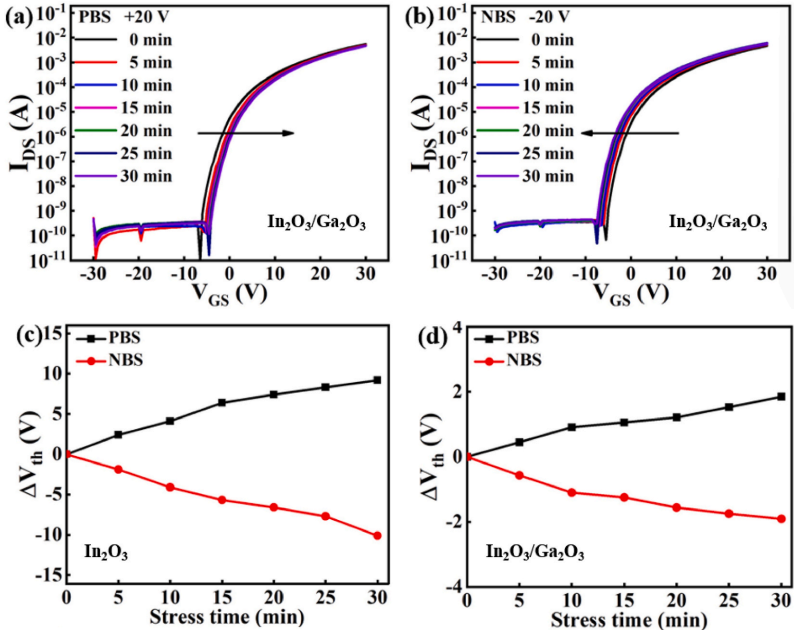
Realization of Fully Solution-Based Low-Power Devices: The team further integrated the passivated In₂O₃ with a solution-processed 6 nm thick high-k ZrO₂ dielectric, successfully constructing fully solution-based two-dimensional oxide transistors that operate excellently at an ultra-low voltage of 1 V.
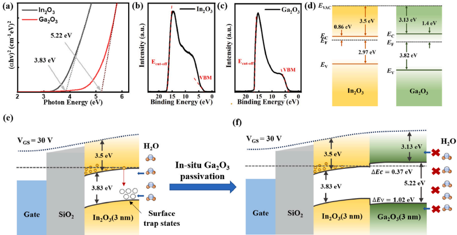
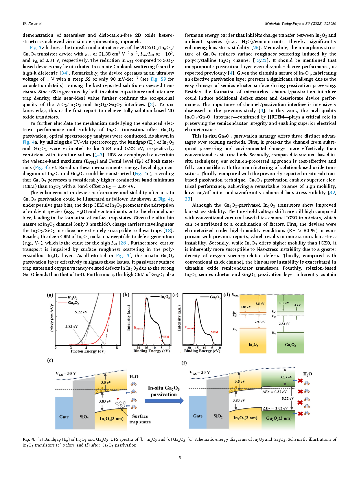
In-Depth Mechanism Elucidation: Band alignment analysis revealed that the high CBM of Ga₂O₃ (conduction band offset ΔEC = 0.37 eV) effectively blocks charge transfer from the environment, the strong Ga-O bonds suppress oxygen vacancy defects, and the amorphous structure reduces surface scattering.
Innovations
Pioneering simultaneous resolution of the mobility-off-state current and mobility-stability trade-offs via in-situ Ga₂O₃ passivation: Unlike traditional doping or ex-situ passivation, this method directly introduces the passivation layer during the solution-based fabrication process, avoiding post-processing contamination without sacrificing mobility.
Integration of fully solution-based 2D oxide transistors: Combining with a solution-processed high-k ZrO₂ dielectric enables low-power, high-performance fully solution-based 2D devices, providing a low-cost path for large-scale manufacturing.
Eco-friendly process: The entire process uses aqueous precursors, avoiding organic solvents, aligning with green manufacturing trends.
Conclusion
This research successfully developed an efficient in-situ ultrathin Ga₂O₃ passivation strategy, decisively breaking the traditional trade-offs between mobility, off-state current, and stability in 2D In₂O₃ transistors. Using an in-situ aqueous solution-processed 3 nm amorphous Ga₂O₃ passivation layer, the mobility (μFE) of the 3 nm In₂O₃ transistor was increased from 32.93 to 45.69 cm² V⁻¹ s⁻¹, the off-state current (Ioff) was suppressed from 10⁻⁶ to 10⁻¹⁰ A, achieving an on/off ratio >10⁸, and the PBS/NBS ΔVth was reduced from ±9 V to ±1.9 V. Combining this with a solution-processed 6 nm ZrO₂ high-k dielectric realized a fully solution-based 2D oxide transistor operating at an ultra-low voltage of 1 V. This scheme offers a simple, green, and economical process, providing a novel technological pathway for developing high-performance, highly reliable back-end-of-the-line (BEOL) 3D integrated electronic devices, holding significant scientific importance and application prospects.