Paper Sharing
【Domestic Papers】Optoelectronic Synaptic Devices Based on ε-Ga₂O₃/ZnO Heterojunctions Grown by an Optimized Process
日期:2025-11-19阅读:415
Researchers from the North China Electric Power University have published a dissertation titled "Optoelectronic Synaptic Devices Based on ε-Ga2O3/ZnO Heterojunctions Grown by an Optimized Process" in Crystal Growth & Design.
Project Support
This work was supported by the National Natural Science Foundation of China (No. 61704054).
Background
ZnO is widely employed in device applications such as UV detectors, light-emitting diodes, solar cells, and piezoelectric sensors owing to its favorable properties, including a wide bandgap, high electron mobility, and piezoelectric characteristics, among others. Despite substantial progress in ZnO thin film growth technologies, significant challenges persist in achieving the cost-effective and efficient deposition of ZnO films with superior crystalline quality and surface integrity. The hexagonal wurtzite structure intrinsic to ZnO generates polar surfaces with an elevated surface energy. This inherent energy predisposition results in predominant island growth patterns during vapor deposition processes, where subsequent island coalescence frequently induces dislocation formation, ultimately yielding columnar or granular microstructures. This phenomenon is particularly pronounced on substrates with a high lattice mismatch, such as sapphire. Although the nanostructured and microstructural characteristics of ZnO have been thoroughly investigated and exploited across diverse applications, comparatively less research attention has been directed toward ZnO thin films.
Abstract
In this study, we introduce a novel methodology, termed the “Growth Process-Synchronized Thermal Injection Method”, aimed at modifying the growth characteristics of ZnO thin films for application in optoelectronic artificial synapses. By incorporation of an ε-Ga2O3 film as an induction layer, Ga ions are introduced in situ during the growth of ZnO thin films. This approach enables the formation of an alloyed induction layer at the growth interface, which significantly reduces lattice mismatch and transforms the growth pattern from island-like to pyramidal. Initially, the unoptimized ZnO films exhibit columnar microstructures composed of dual crystalline phases and lack a dominant crystallographic orientation on their surfaces. However, after the growth habit is modified, the resulting ZnO films display single-phase characteristics with a distinct preferred orientation on out-of-plane crystal orientation. Optoelectronic synapses were engineered using heterojunctions formed between ε-Ga2O3 films and the optimized ZnO films, demonstrating the ability to emulate various synaptic behaviors, including short-term memory, long-term memory, forgetting, recall, and environment-modulated memory, thereby underscoring the potential of this architecture for brain-inspired computing. In summary, the proposed “Growth Process-Synchronized Thermal Injection Method” not only offers an effective strategy for enhancing the crystalline quality of ZnO thin films but also provides valuable insights into the manipulation of growth mechanisms for improving the structural and functional properties of other thin film materials. Moreover, the optoelectronic artificial synapses based on oxygen vacancy defects within ε-Ga2O3/ZnO heterojunctions exhibit robust synaptic behaviors and serve as a reference for future development and practical applications of optoelectronic devices incorporating such heterojunctions.
Conclusion
Through the incorporation of a ε-Ga2O3 induction layer, we effectively controlled the growth mode of ZnO from island-like to pyramidal morphology. Consequently, this transformation led to the conversion of the initially disordered microstructure into a planar film with an improved crystal quality and enhanced surface properties. The resultant ZnO films exhibit well-defined step structures on their surfaces and a unidirectional growth orientation. Furthermore, these films display remarkably narrow rocking curves with half-widths as low as 551 arcsec and minimal surface roughness values of 7.38 nm. Based on these significant observations, we propose a novel approach termed the “growth process-synchronized thermal injection method”, which is further supported by our comprehensive elucidation using EDS spectroscopy analysis. We hypothesize that, in the presence of a reducing atmosphere and high-temperature environment, Ga2O3 and ZnO undergo mutual thermal injection, predominantly involving Ga ions. This thermal injection facilitates the formation of a homogeneous alloy induction layer on the growth surface. Consequently, under the influence of this alloy induction layer, lattice mismatch is mitigated, inducing a transition from the island growth mode to the pyramidal growth mode. The “growth process-synchronized thermal injection method” provides a pathway for optimizing the growth of ZnO thin films and offers novel insights into modifying the growth behavior of other materials to achieve superior film quality. Subsequently, we fabricated optoelectronic artificial synapses using the optimized ε-Ga2O3/ZnO heterojunction, which successfully mimicked the synaptic behaviors of short-term memory, long-term memory, relearning, and environmental influences, providing a valuable reference for the research of optoelectronic devices with ε-Ga2O3/ZnO heterojunctions.
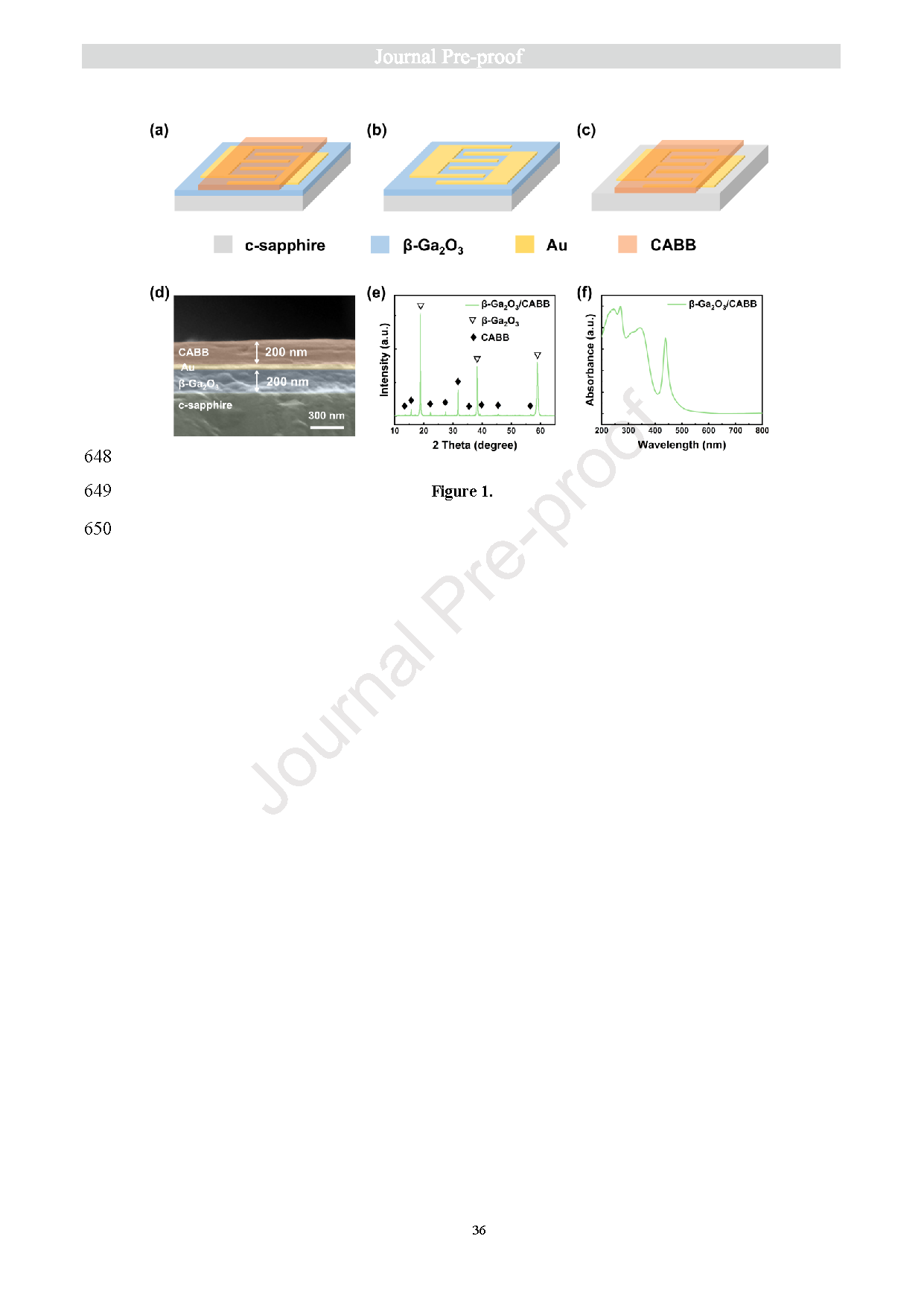
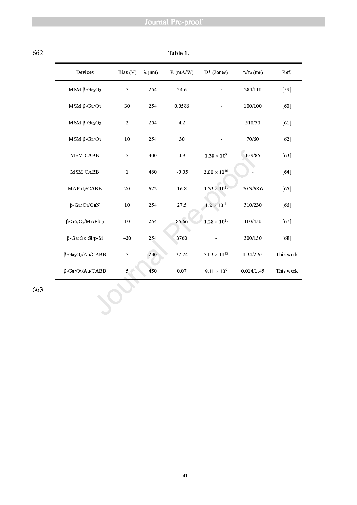
Figure 1. (a−c) XRD patterns of ε-Ga2O3, ZnO (direct growth) and ZnO (induction layer) and (d−f) Raman spectral patterns of ε-Ga2O3, ZnO (direct growth), and ZnO (induction layer).
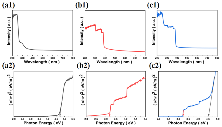
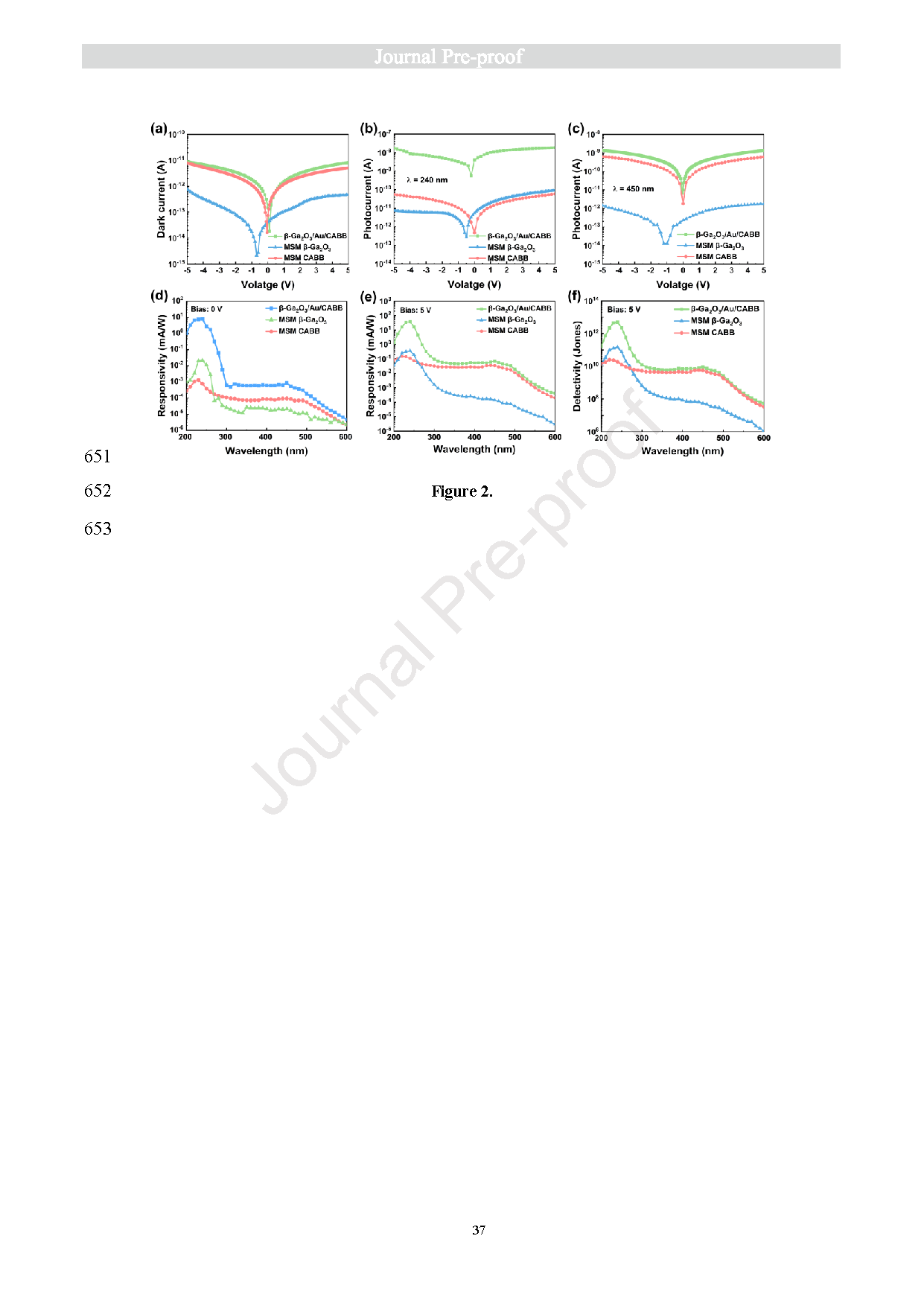
Figure 2. (a1−c1) UV−vis absorption spectra of ε-Ga2O3, ZnO (direct growth), and ZnO (induction layer) and (a2−c2) forbidden bandwidths of ε-Ga2O3, ZnO (direct growth), and ZnO (induction layer).
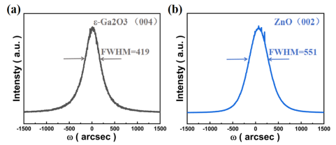
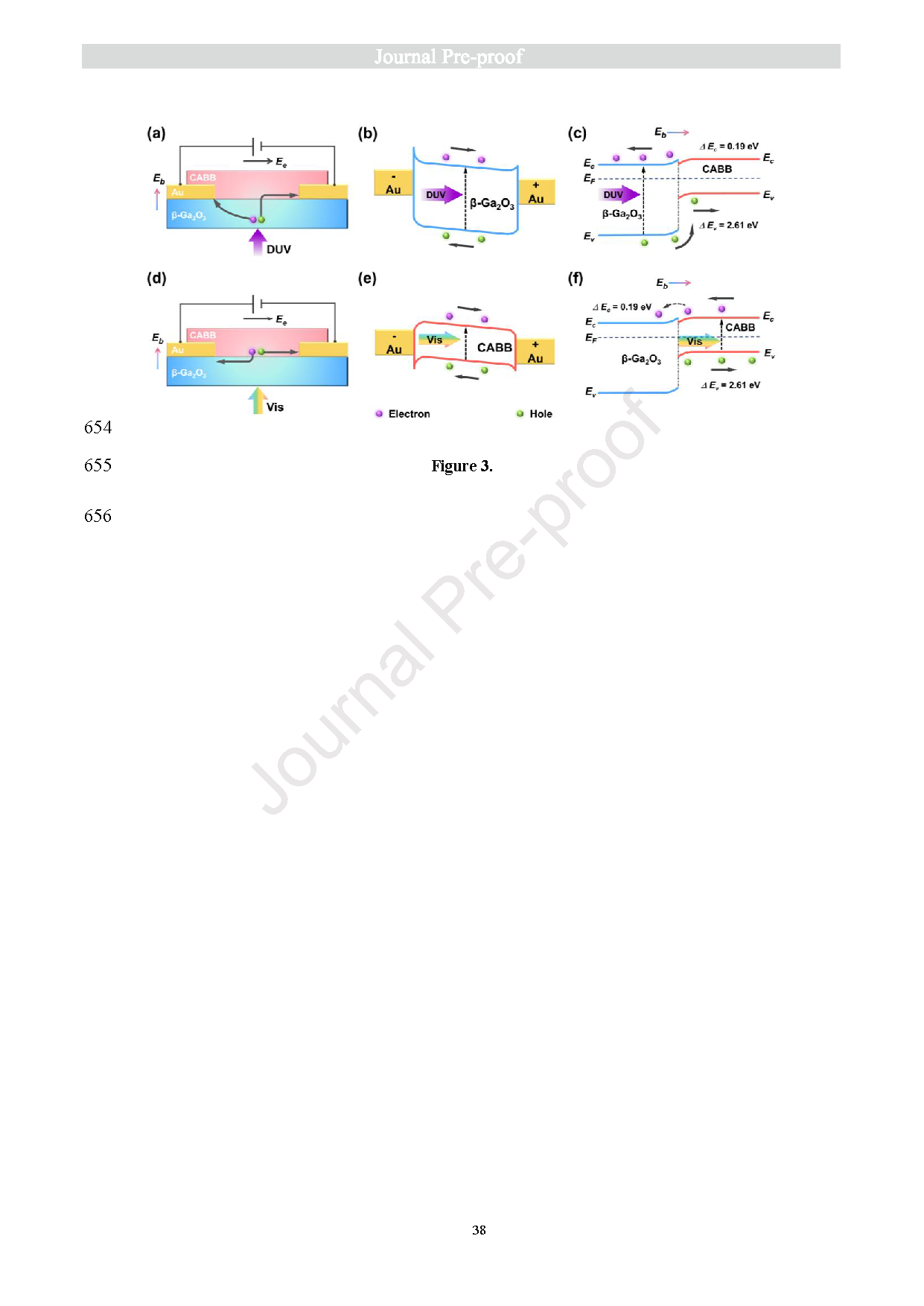
Figure 3. (a) (004) Surface rocking profile of the ε-Ga2O3 film and (b) (002) surface rocking profile of ZnO (induction layer).
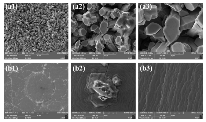
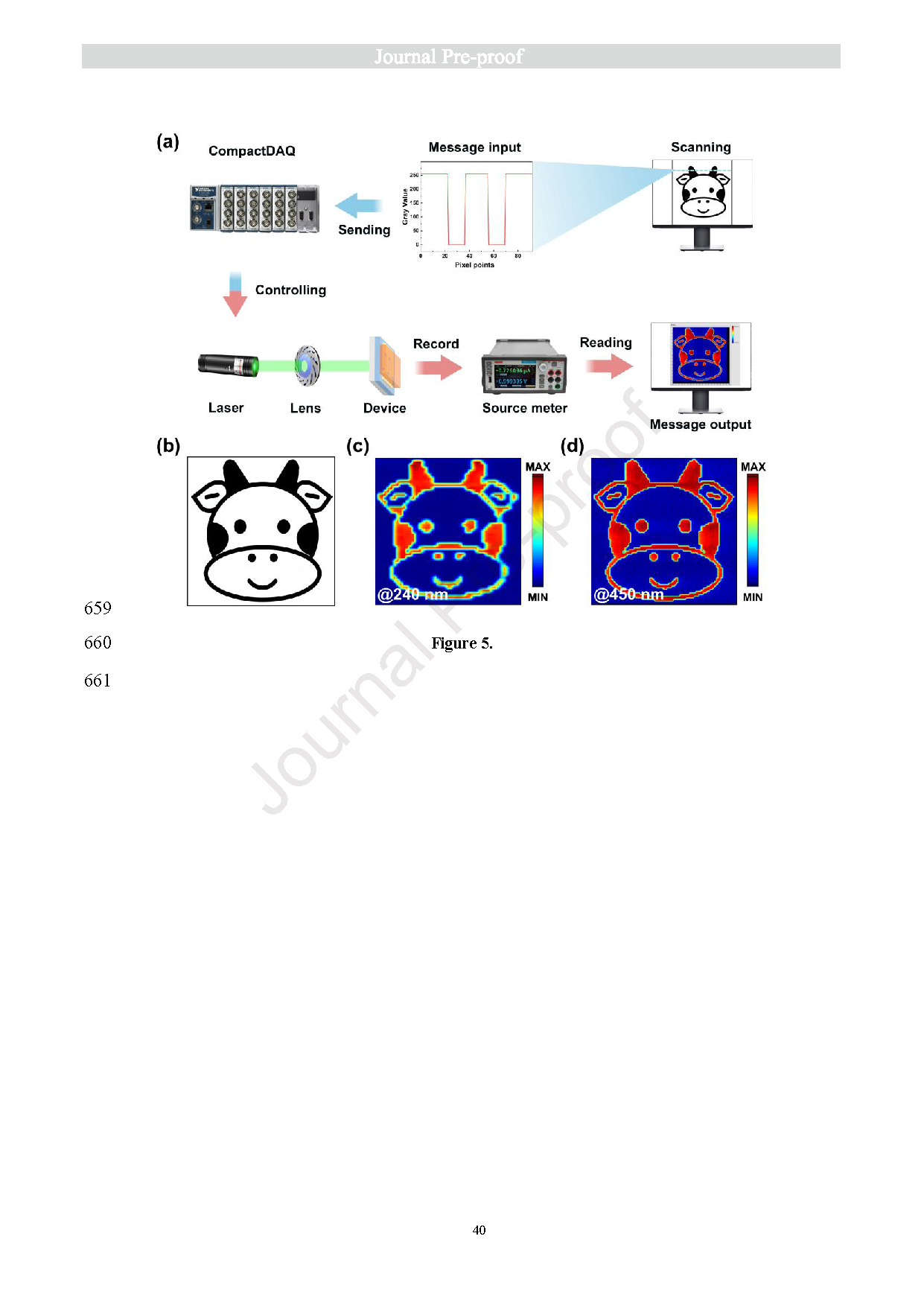
Figure 4. Surface morphology of (a1−a3) ZnO (direct growth) and (b1−b3) ZnO (induction layer) (1000×, 5000×, and 10000×).

Figure 5. Surface topography of samples measured by AFM (a) ε-Ga2O3, (b) ZnO (direct growth), (c) ZnO (induction layer) small scan, and (d) height profile of the blue straight line in (c).
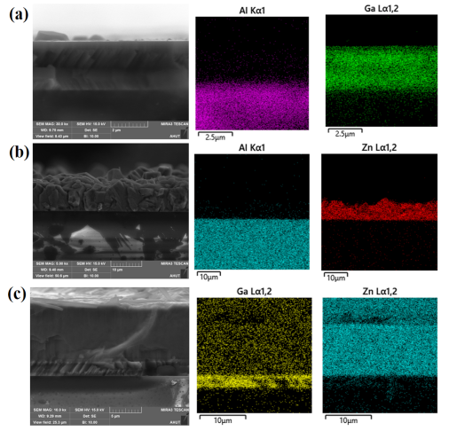
Figure 6. Cross sections of thin films and corresponding EDS energy spectra: (a) ε-Ga2O3, (b) ZnO (direct growth), and (c) ZnO (induction layer).
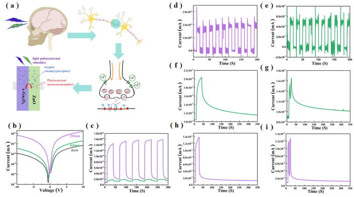
Figure 7. (a) Schematic diagram of artificial synapses of the ε-Ga2O3/ZnO heterojunction. (b) Output curves of the heterojunction in darkness, 254, and 365 nm light illumination. (c) Photoresponse curves of the heterojunction in 254 and 365 nm light illumination (10 V positive bias). (d) Self-powering curves with 254 nm pulsed light signals. (e) 365 nm pulsed light signals with self-powered curves. (f) 365 nm single-pulse (30S) light signal. (g) Paired-pulse facilitation (10S) for 365 nm double-pulse light signal. (h) 254 nm single-pulse (30S) light signal. (i) Paired-pulse facilitation (10S) for 254 nm double-pulse light signal.
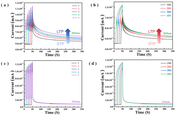
Figure 8. Memristive properties after 365 nm illumination: (a) different numbers of pulses and (b) different illumination times. 254 nm illumination: (c) different numbers of pulses and (d) different illumination times.
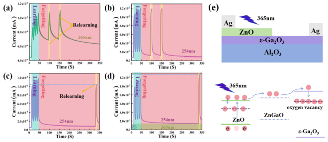
Figure 9. (a) Behavioral simulation of “forgetting (50S) and relearning” under 365 nm light. (b) Behavioral simulation of “forgetting (50S) and relearning” under 254 nm light. (c) Behavioral simulation of “forgetting (280S) and relearning” under 254 nm light. (d) Behavioral simulation of “forgetting (280S) and relearning” using 254 nm pulsed light representing high-intensity stimuli under the continuous presence of 365 nm light. (e) Principle of the effect of 365 nm light persisting on the resistance.
DOI:
doi.org/10.1021/acs.cgd.5c00641