


Paper Sharing
【Member Papers】Achievement of High-Quality Gallium Oxide Epitaxial Growth via Machine Learning
日期:2025-11-18阅读:385
Researchers from the Fuzhou University, Shanghai Institute of Optics and Fine Mechanics, Chinese Academy of Sciences, have published a dissertation titled " Achievement of High-Quality Gallium Oxide Epitaxial Growth via Machine Learning " in Advanced Functional Materials.
Project Support
This work was supported by the following funding programs: the National Natural Science Foundation of China (Grant Nos. 62204270 and 62501162), the Natural Science Foundation of Fujian Province (Grant No. 2024J01251), the Major Science and Technology Project of Fujian Province (Grant No. 2024HZ027006), the Fujian Provincial Science and Technology Program (Grant No. 2022I0006), the Fujian Provincial Young and Middle-aged Teachers’ Education and Research Project (Grant No. JAT220020), and the Quanzhou Science and Technology Bureau Major Science and Technology Project (Grant No. 2022GZ04).
Background
Gallium Oxide (Ga₂O₃), with its ultrawide bandgap (4.5–4.9 eV) and high critical breakdown field (~8 MV/cm), is considered an ideal material for next-generation high-voltage and low-loss power devices. These application requirements impose stringent demands on the crystalline quality of Ga₂O₃ epitaxial layers. A key challenge for the industrialization of Ga₂O₃ is how to efficiently and cost-effectively prepare high-quality homoepitaxial layers.
The development of Ga₂O₃ materials is still in its early stage. Due to the lack of well-established heteroepitaxial growth theories and the narrow process window, it remains a significant challenge to produce wafer-scale epitaxial films grown in the “step-flow” mode using low-cost approaches. Although metal–organic chemical vapor deposition (MOCVD) is highly regarded for its ability to produce high-quality epitaxial layers, the “pre-reaction” issue during Ga₂O₃ epitaxy significantly narrows the available process window for high-quality growth. Moreover, MOCVD involves numerous process parameters that interact and constrain one another. Traditional trial-and-error approaches to process development inherently suffer from long development cycles, high cost, and heavy dependence on engineers’ subjective experience.
Therefore, it is essential to develop an approach that regulates thermodynamic and kinetic parameters within the epitaxial system to achieve high-quality Ga₂O₃ homoepitaxial layers in an efficient and cost-effective manner.
Abstract
The development of gallium oxide (Ga2O3)-based electronics has been hampered by the persistent challenge of obtaining high-quality epilayers with device-grade performance metrics. While metal-organic chemical vapor deposition has proven effective in producing device-grade films, the realization of ideal step-flow epitaxial growth with high deposition rates in Ga2O3 remains a significant scientific challenge. Here, a machine learning (ML)-guided approach is presented to overcome conventional epitaxial limitations, which are historically constrained by narrow process windows and empirical growth paradigms. Specifically, our ML-guided approach successfully achieves perfect step-flow epitaxy at 1.2 µm h−1 on universal β-Ga2O3 substrates, eliminating traditional requirements for large mis-cut angle substrates and low growth rates. This breakthrough resolves the long-standing trade-off between crystal quality and growth efficiency. The resultant epilayers exhibit atomically smooth surfaces with record-low roughness (0.121 nm) featuring 6 Å-high single-atomic-layer steps, coupled with exceptional electrical properties. The technological viability is further validated through Schottky barrier photodiodes with excellent solar-blind detection performance: ultra-fast decay time (3.28 µs), ultra-high photo-to-dark current ratio (PDCR > 105), and ultralow dark current density (6.2 × 10⁻⁹ A cm−2). This work not only establishes ML as a revolutionary accelerator for β-Ga2O3 development but also provides a transformative methodology for next-generation semiconductor manufacturing.
Figure 1 (a) Photograph of a 2-inch high-quality β-Ga₂O₃ homoepitaxial wafer. (b) Epita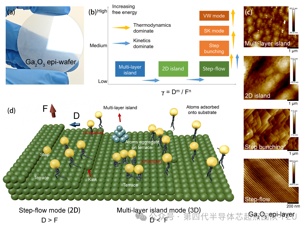 xial growth phase diagram constructed from thermodynamic and kinetic perspectives. The y-axis represents the system free energy, and the x-axis represents the key growth factor γ, which is determined by the thermal diffusion coefficient D and total deposition rate F. (c) Atomic force microscopy (AFM) images of four growth modes of β-Ga₂O₃ homoepitaxy: multilayer island, 2D island, step-bunching, and step-flow. In this work, the surface morphologies associated with multilayer island, 2D island, and step-bunching modes are consistent with historical results, while the step-flow mode is achieved through machine-learning-assisted (ML-guided) process optimization. (d) Schematic of the TSK model describing the kinetic processes of step-flow and multilayer island growth modes. Modern epitaxy theory indicates that realizing step-flow growth requires satisfying the conditions of a mass-transport-limited regime.
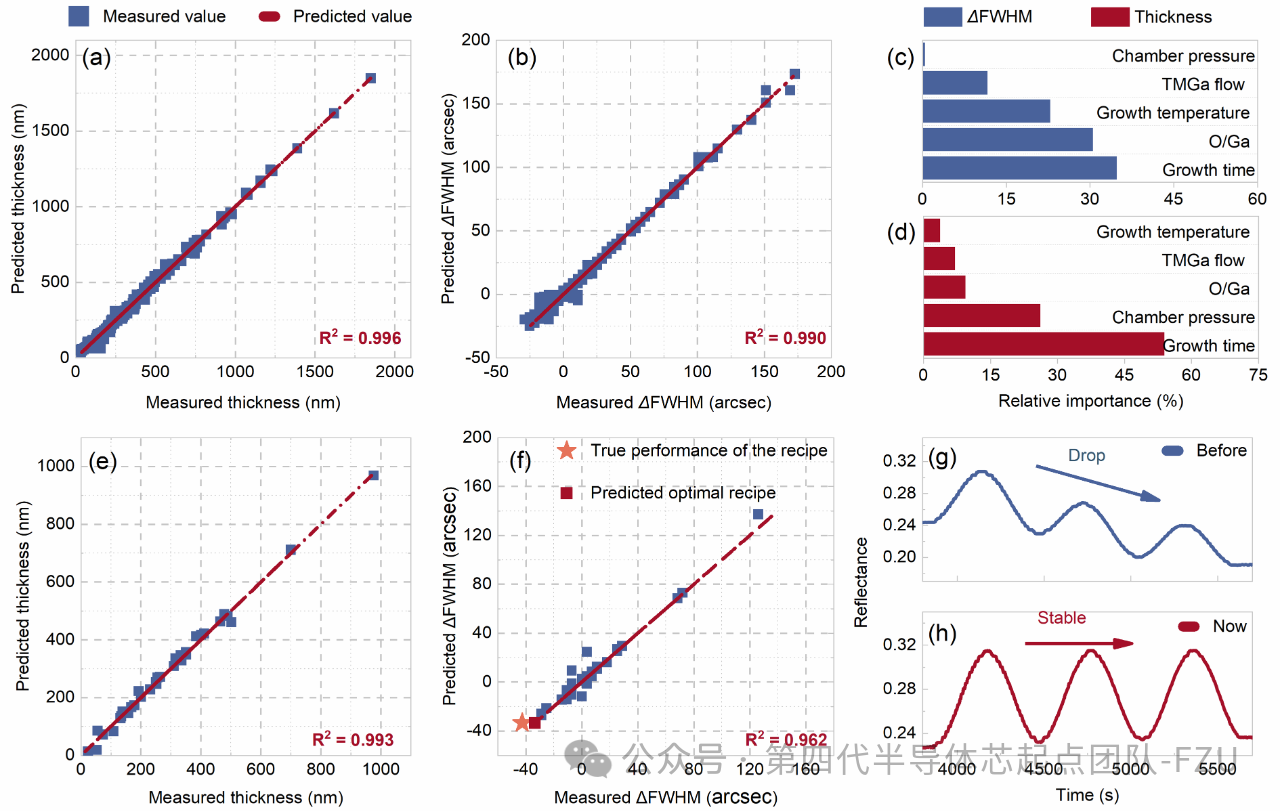
Figure 2 (a) Fitting results of film thickness for the training dataset, with a coefficient of determination R² = 0.996. (b) Fitting results of full width at half maximum (FWHM) for the training dataset, with R² = 0.990. Blue circles represent measured data and red dashed lines represent model predictions. R² quantifies the goodness of fit; smaller deviation indicates closer agreement between prediction and measurement, and values approaching 1.000 reflect stronger model performance. (c) Influence of epitaxy parameters on ΔFWHM (change in FWHM). (d) Influence of epitaxy parameters on film thickness. In the polynomial regression model, x denotes the explanatory vector, including chamber pressure, trimethylgallium (TMGa) flow rate, growth temperature, O/Ga ratio, and growth time. The fitted model reveals how these parameters collectively affect epitaxial thickness and crystalline quality. (e) Film-thickness fitting for the test dataset, R² = 0.993. (f) FWHM fitting for the test dataset, R² = 0.962. Again, blue circles denote measurements, red dashed lines denote predictions. The optimal process recipe predicted by the model is marked with a red square, and the corresponding experimentally grown sample is marked with an orange pentagram. The high R² values on the test dataset demonstrate excellent predictive accuracy and reliability of the model, confirming its robust interpretability for epitaxial processes.(g) In-situ reflectance interference curve without ML-assisted process optimization. (h) In-situ reflectance interference curve after ML-assisted optimization. The interference pattern originates from laser reflections at the epitaxial surface and reflects growth rate and surface roughness. A pronounced drop in reflectance indicates severe surface roughening. Under the same growth rate, the absence of reflectance decay shows that ML optimization significantly improves epitaxial conditions.

Figure 3 (a) Determination of the unintentional miscut direction and miscut angle of the substrate using combined X-ray diffraction (XRD) and X-ray reflectivity (XRR). For a β-Ga₂O₃ substrate with a miscut direction from [100] toward [00-1], the lowest point of the fitted sinusoidal function appears at 270°, where the vertical coordinate corresponds to the miscut angle. In this sample, the minimum does not occur at 270°, indicating that the unintentional miscut direction is not from [100] toward [00-1]. (b) XRD spectrum of β-Ga₂O₃ heteroepitaxial layers grown on sapphire. Inset: high-resolution rocking curves of the symmetric (400) reflection for β-Ga₂O₃ homoepitaxy on a β-Ga₂O₃ (100) substrate. The FWHM values of the substrate and epitaxial layer are 108 and 57.6 arcsec, respectively. (c) Optical bandgap extracted using the Tauc method. (d) X-ray reciprocal space map (RSM) of the homoepitaxial layer grown on a miscut β-Ga₂O₃ substrate. (e) AFM image of the homoepitaxial layer over a 10 × 10 μm² area. The surface exhibits uniform step-flow morphology; however, due to the extremely fine steps generated during growth, they cannot be resolved at this scale, appearing only as ultralow surface roughness. (f) AFM image and step height over a 3 × 3 μm² area, clearly revealing the highly regular and uniform step-flow morphology. (g) ΔFWHM distribution map of the 2-inch β-Ga₂O₃ homoepitaxial wafer. Measurements were performed along four diameters spaced 45° apart, with nine sampling points on each diameter. (h) High-resolution transmission electron microscopy (HRTEM) image of the β-Ga₂O₃ homoepitaxial layer. The lattice spacings of the (200) and (110) planes are d(200) = 5.91 Å and d(110) = 2.92 Å, respectively. (i) Selected-area electron diffraction (SAED) pattern of the β-Ga₂O₃ homoepitaxial layer taken along the [00-1] zone axis.
DOI:
https://doi.org/10.1002/adfm.202519854
