Paper Sharing
【Domestic Papers】Towards solar-blind ultraviolet signal visualization of photodetection and electroluminescenc integrated devices through Er doping
日期:2025-11-18阅读:414
Researchers from the Huanghe Science and Technology College have published a dissertation titled "Towards solar-blind ultraviolet signal visualization of photodetection and electroluminescenc integrated devices through Er doping" in Journal of Alloys and Compounds.
Project Support
This work was financed by the Zhengzhou Municipal Basic Research and Applied Basic Research Special Fund Project (Project No. ZZSZX202402), the Program for Science & Technology Innovation Talents in Universities of Henan Province (24HASTIT002), and the Doctoral Start-up Fund of Huanghe Science and Technology College (Project No. 0203240058).
Background
Solar radiation in the solar-blind ultraviolet (UV, 200–280 nm) band is completely absorbed by the ozone layer of the Earth's atmosphere, resulting in a low solar background noise in this wavelength for light detection. Consequently, the solar-blind UV photodetector could obtain a high signal-to-noise ratio at work, which is widely applied in space communication, missile early warning, UV imaging, fire detectors, etc. With the development of modern industry and defense science and technology, the market demand for high sensitivity, high stability, and high response speed of the solar-blind ultraviolet detector is increasingly urgent, which has greatly promoted the research on new wide-band semiconductor materials and devices. Gallium oxide (Ga2O3) has a large bandgap width of ∼4.8 eV, corresponding to the deep UV wavelength region for light absorption.
Abstract
The Ga2O3-based solar-blind ultraviolet photodetectors have important application potential in the flame and arc detection fields, but the device performance is limited by the poor crystalline quality and high dark current. Meanwhile, integrating multiple optoelectronic functions helps reduce the device size and improve the feedback speed. Rare earth doping, as an effective optimization strategy, could not only improve the photoresponse performance of photodetectors but also endow them with electroluminescence functionality. Herein, a strategy of decomposing organic precursors was developed to synthesize Er-doped Ga2O3 (Ga2O3:Er) films, and the Ga2O3:Er/SiO2/p-Si heterojunction devices were constructed. The photodetector performance was improved by reducing the dark current, suppressing the oxygen defects, and increasing the shallow-level trap concentration. The device reached a responsivity, detectivity, and response time of ∼5.25 × 10³ mA W−1, ∼3.67 × 10¹⁴ Jones, and ∼50 μs under 254 nm light irradiation, respectively. The Er-related electroluminescence of the device under high reverse voltage could be attributed to the impact of hot electrons induced by Zener-tunneling-dominated electrical transport behavior. Such photodetection and electroluminescence integrated devices enable optical-to-electrical-to-optical signal conversion and visualization of ultraviolet signals. This work is significant for developing high-performance solar-blind ultraviolet detectors and multifunctional integrated devices.
Highlights
• Novel and flexible method for synthesizing Ga₂O₃-based thin films.
• Er doping can significantly improve the performance of Ga₂O₃-based solar-blind ultraviolet detectors.
• The device reached a detectivity of ∼3.67 × 10¹⁴ Jones under 254 nm light irradiation.
• Devices with the same structure exhibit characteristic EL performance of rare earth ions under reverse voltages.
• The integrated devices enable optical-to-electrical-to-optical signal conversion and visualization of ultraviolet signals.
Conclusion
In summary, a universal and flexible method for synthesizing undoped and RE-doped Ga2O3 films has been developed to construct Ga2O3-related optoelectronic devices. The Er doping can improve the crystalline quality, reduce oxygen defects, narrow the bandgap, and increase the concentration of shallow-level traps of Ga2O3, thereby suppressing the dark current and improving the photoresponse performance of UV photodetectors. The constructed device has a response R, specific detectivity D*, and response time of ~5.25 × 10³ mA W− 1, ~3.67 × 10¹⁴ Jones, and ~50 μs, respectively, under a 254 nm light irradiation and at − 1 V. Meanwhile, the device exhibits RE-related EL behavior under high reverse voltage, which can be attributed to the collision excitation of RE ions by hot electrons derived from Zener-tunneling-dominated electrical transport behavior. Moreover, the RE related EL behavior of the device is affected by external light illumination through changes in current. Therefore, the device can convert signals from light to electricity to light under UV light or electric arc irradiation. This work provides new insights into the development of high-performance solar-blind UV detectors, the functional integration of photoresponse and EL, and the visible feedback of UV signals.
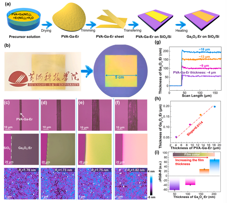
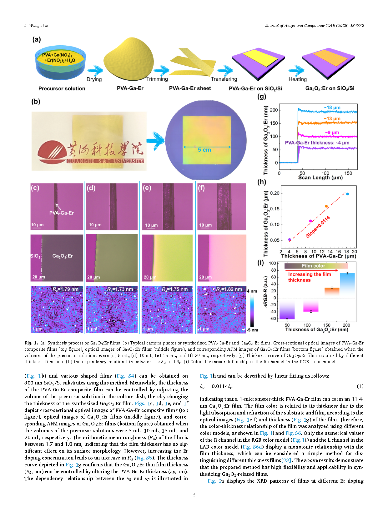
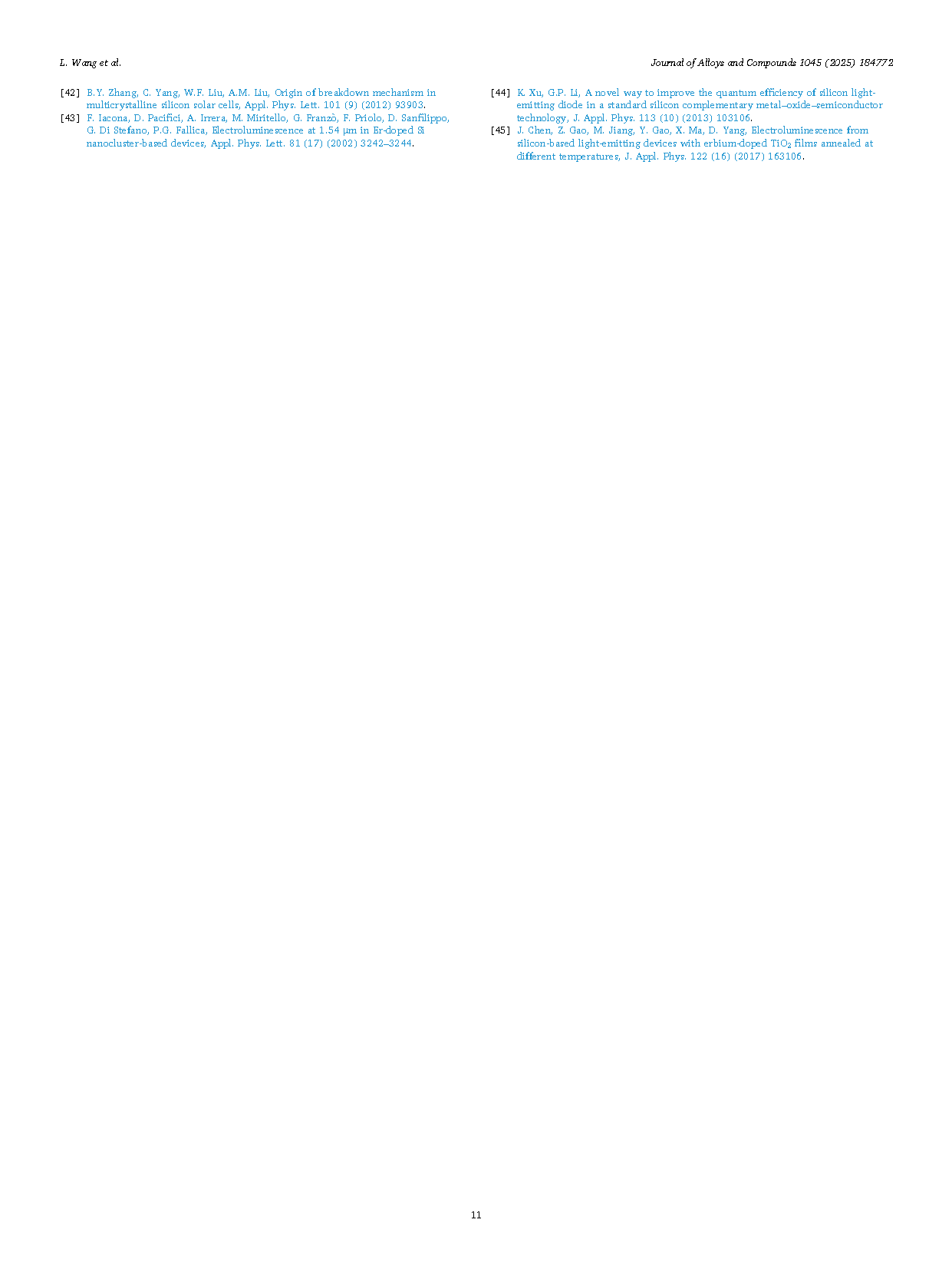
Fig. 1. (a) Synthesis process of Ga2O3:Er films. (b) Typical camera photos of synthesized PVA-Ga-Er and Ga2O3:Er films. Cross-sectional optical images of PVA-Ga-Er composite films (top figure), optical images of Ga2O3:Er films (middle figure), and corresponding AFM images of Ga2O3:Er films (bottom figure) obtained when the volumes of the precursor solutions were (c) 5 mL, (d) 10 mL, (e) 15 mL, and (f) 20 mL, respectively. (g) Thickness curve of Ga2O3:Er films obtained by different thickness films and (h) the dependency relationship between the δG and δP. (i) Color-thickness relationship of the R channel in the RGB color model.
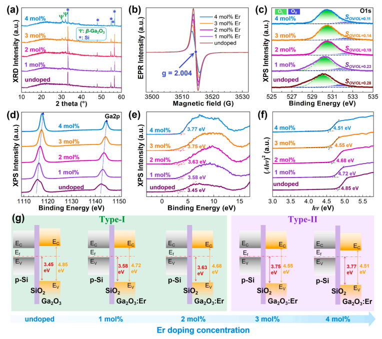
Fig. 2. (a) XRD patterns, (b) EPR spectra, (c) XPS O1s spectra, (d) XPS Ga2p spectra, (e) valence band spectra, and (f) curves derived from the absorption spectra of films at different Er doping concentrations. (g) Band characteristics of the heterojunction at different Er doping concentrations.
Fig. 3. TEM images of (a) undoped Ga2O3 and (b) Ga2O3:Er nanomaterials, respectively. HRTEM images of (c) undoped Ga2O3 and (d) Ga2O3:Er nanomaterials, respectively. Diffraction patterns of (e) undoped Ga2O3 and (f) Ga2O3:Er nanomaterials, respectively. (g) High-angle annular dark-field image and different element distributions of Ga2O3:Er nanomaterials.
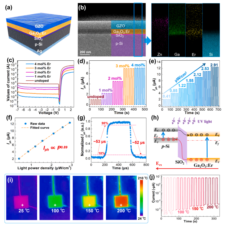
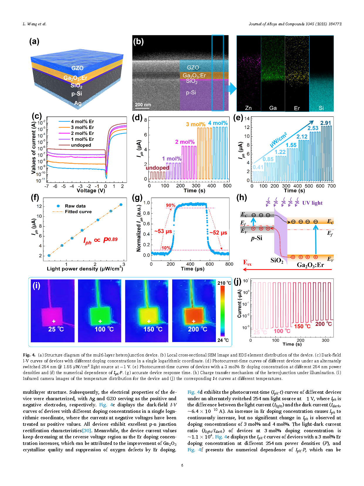
Fig. 4. (a) Structure diagram of the multi-layer heterojunction device. (b) Local cross-sectional SEM image and EDS element distribution of the device. (c) Dark-field I-V curves of devices with different doping concentrations in a single logarithmic coordinate. (d) Photocurrent-time curves of different devices under an alternately switched 254 nm @ 1.55 μW/cm2 light source at − 1 V. (e) Photocurrent-time curves of devices with a 3 mol% Er doping concentration at different 254 nm power densities and (f) the numerical dependence of Iph-P. (g) accurate device response time. (h) Charge transfer mechanism of the heterojunction under illumination. (i) Infrared camera images of the temperature distribution for the device and (j) the corresponding I-t curves at different temperatures.
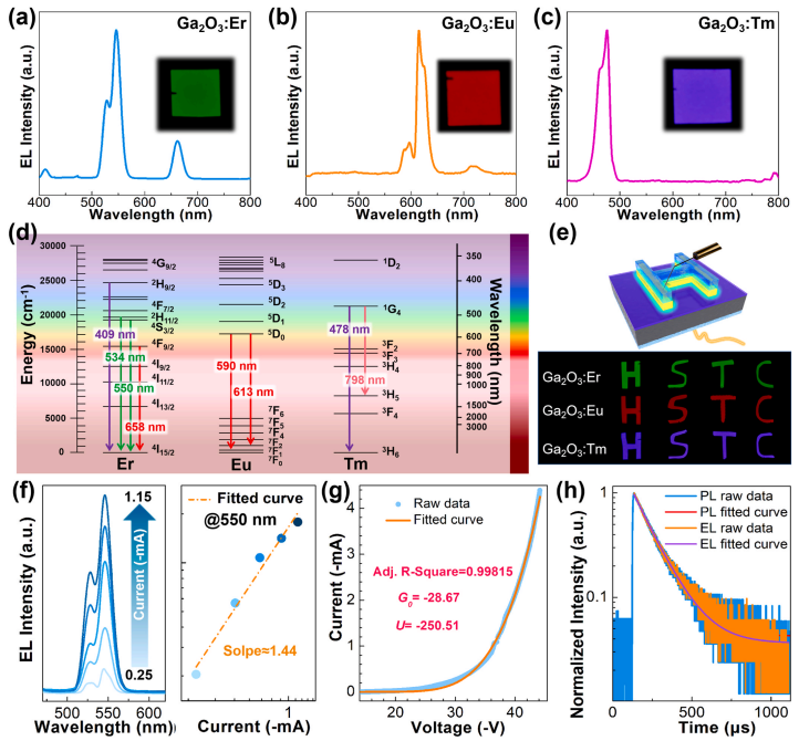
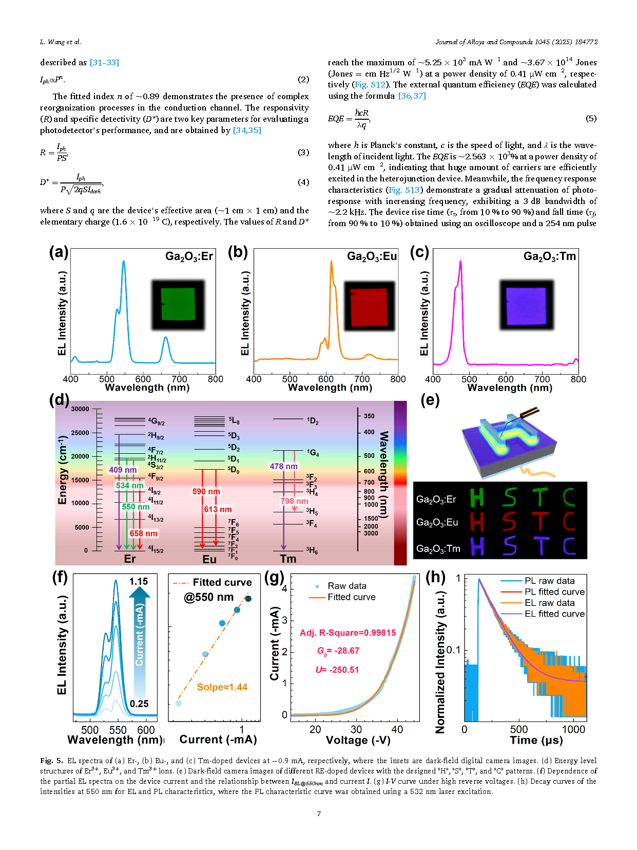
Fig. 5. EL spectra of (a) Er-, (b) Eu-, and (c) Tm-doped devices at − 0.9 mA, respectively, where the insets are dark-field digital camera images. (d) Energy level structures of Er3+, Eu3+, and Tm3+ ions. (e) Dark-field camera images of different RE-doped devices with the designed "H", "S", "T", and "C" patterns. (f) Dependence of the partial EL spectra on the device current and the relationship between IEL@550nm and current I. (g) I-V curve under high reverse voltages. (h) Decay curves of the intensities at 550 nm for EL and PL characteristics, where the PL characteristic curve was obtained using a 532 nm laser excitation.
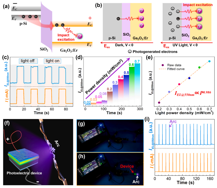
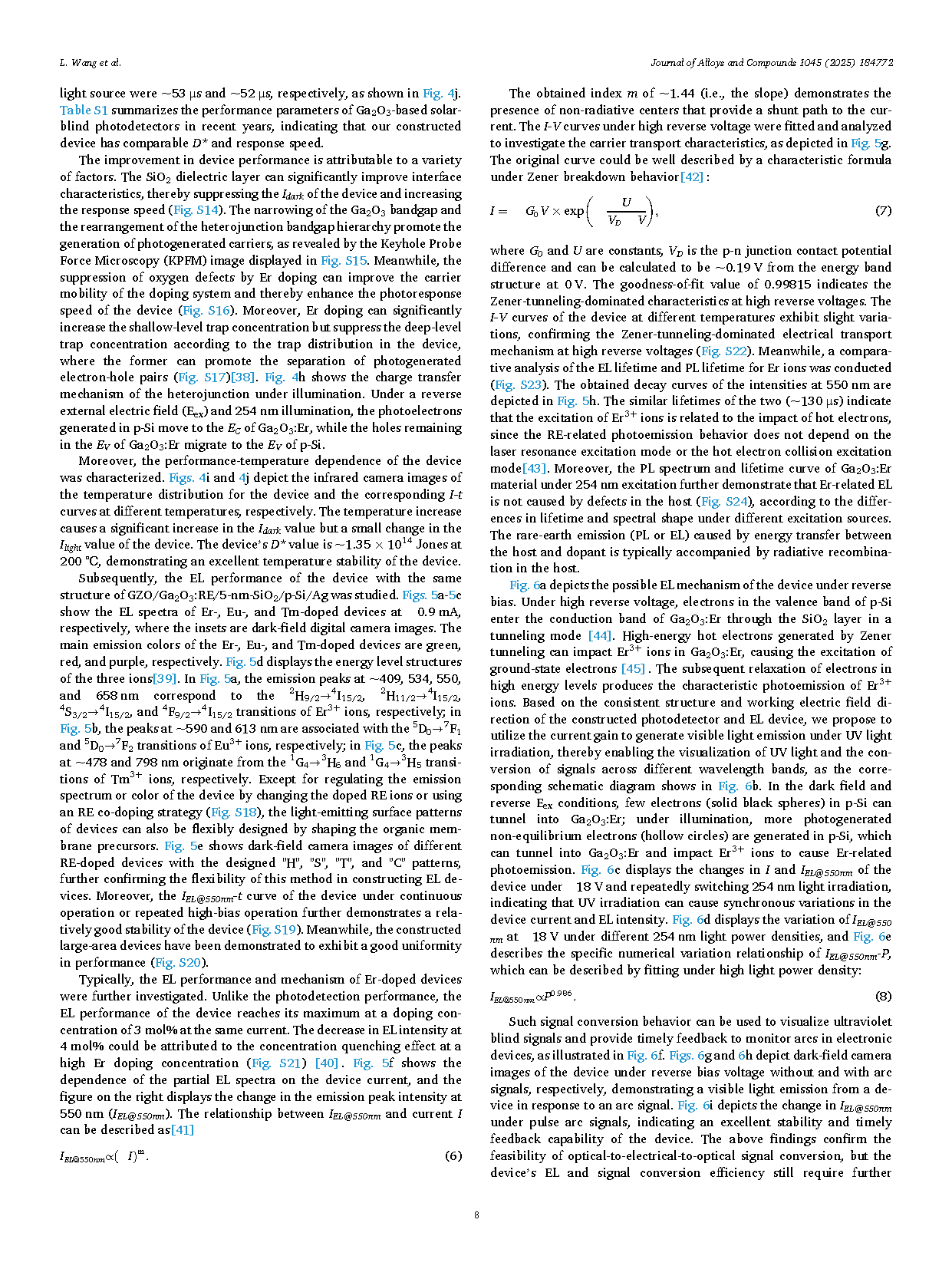
Fig. 6. (a) Possible EL mechanism of the device under reverse voltages. (b) Corresponding schematic diagram for enabling the visualization of UV light and the conversion of signals across different wavelength bands. (c) Changes in I and IEL@550nm of the device under − 18 V and repeatedly switching 254 nm light irradiation. (d) Variation of IEL@550nm at − 18 V under different 254 nm light power densities and (e) the specific numerical variation relationship of IEL@550nm-P. (f) Corresponding schematic diagram for enabling the visualization and timely feedback to monitor arcs in electronic devices. Dark-field camera images of the device under reverse bias voltage (g) without and (h) with arc signals. (i) Changes in IEL@550nm and current I under pulse arc signals.
DOI:
doi.org/10.1016/j.jallcom.2025.184772