Paper Sharing
【Member Papers】Wafer-scale high-performance flexible solar-blind ultraviolet photodetectors based on a-Ga₂O₃ grown by MOCVD
日期:2025-11-17阅读:466
Researchers from the University of Science and Technology of China have published a dissertation titled "Wafer-scale high-performance flexible solar-blind ultraviolet photodetectors based on a-Ga2O3 grown by MOCVD" in Journal of Materials Science & Technology.
Project Support
This work was supported by Suzhou Critical Core Technology Research Project (No. SYG2024003), National Key Research and Development Program of China (No. 2021YFC2203400 ), Key Laboratory Construction Project of Nan chang (No. 2020-NCZDSY-008), Stu- dents’Innovation and Entrepreneurship Foundation of USTC (No. CY2023 × 001), the Nano Fabrication Facility, center of characterization & analysis and Vacuum Inter- connected Nanotech Workstation (NANO-X) of Suzhou Institute of Nano-Tech and Nano-Bionics, Chinese Academy of Sciences.
Background
Solar-blind deep ultraviolet photodetectors (UVPDs), operating in the 200–280 nm wavelength range, are widely used in fields such as space exploration, environmental monitoring, and missile plume detection. While Ga₂O₃ devices on rigid substrates exhibit excellent performance, they are limited in applications requiring flexibility, such as wearable electronics and flexible devices. Amorphous Ga₂O₃ (a-Ga₂O₃) thin films, with their disordered atomic arrangement and lack of long-range lattice order, offer superior mechanical adaptability, making them suitable for flexible UVPDs. However, deep-level defects such as oxygen vacancies (Vo) readily form in a-Ga₂O₃, causing carrier trapping, persistent photoconductivity (PPC), increased dark current, and delayed device response, which significantly degrade performance. Additionally, surface roughness of flexible substrates can introduce further defects in the deposited films, further limiting device quality.
Therefore, achieving large-area, high-performance flexible a-Ga₂O₃ UVPDs requires both defect engineering (e.g., reducing Vo concentration) and optimized device fabrication processes. By employing an oxygen-rich growth strategy to increase oxygen flow during MOCVD and combining it with wafer-scale film transfer techniques, 4-inch flexible metal–semiconductor–metal (MSM) UVPDs have been realized. These devices demonstrate high responsivity, excellent external quantum efficiency, fast transient response, and robust mechanical flexibility and environmental stability before and after substrate transfer, providing a practical and scalable approach for the development of flexible ultraviolet photodetectors.
Abstract
Flexible ultraviolet photodetectors are widely investigated for applications in wearable electronics and environmental monitoring due to their lightweight characteristics and compatibility with complex surfaces. Amorphous gallium oxide (a-Ga2O3), with its wide bandgap of 4.9 eV, is highly suitable for flexible solar-blind UV detection. However, deep-level defects such as oxygen vacancies have long degraded the performance of a-Ga2O3-based flexible detectors. In addition, achieving large-area flexible devices remains challenging, which continues to constrain their development. Herein, an oxygen-rich design strategy is employed to shorten the device response time to 4.3/11.2 ms, suppress the dark current from 6.9 to 0.3 μA, and enhance the detector bandwidth up to 600 dB. The 4-inch wafer-scale flexible a-Ga2O3 detectors are realized by leveraging mechanical thinning and wet etching processes. Remarkably, the devices exhibited highly consistent performance before and after transfer, as well as under repeated bending at various angles and temperature variations. Furthermore, a large-area flexible detector array comprising 144 pixels is fabricated, and high-contrast ultraviolet imaging is successfully demonstrated. This study provides a significant reference for the development of high-performance, wafer-scale a-Ga2O3-based flexible detectors.
Highlights
● Wafer-scale flexible ultraviolet detectors made from amorphous gallium oxide.
● Oxygen-rich design cuts dark current from 6.9 μA to 0.3 μA.
● Fast response (4.3/11.2 ms) and high bending/thermal stability.
● 144-pixel flexible array enables high-contrast ultraviolet imaging.
Conclusion
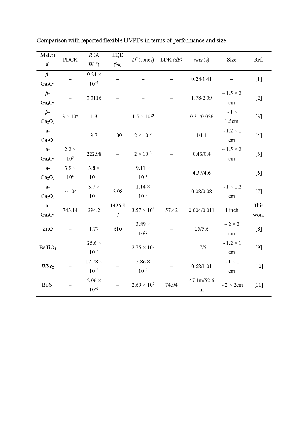
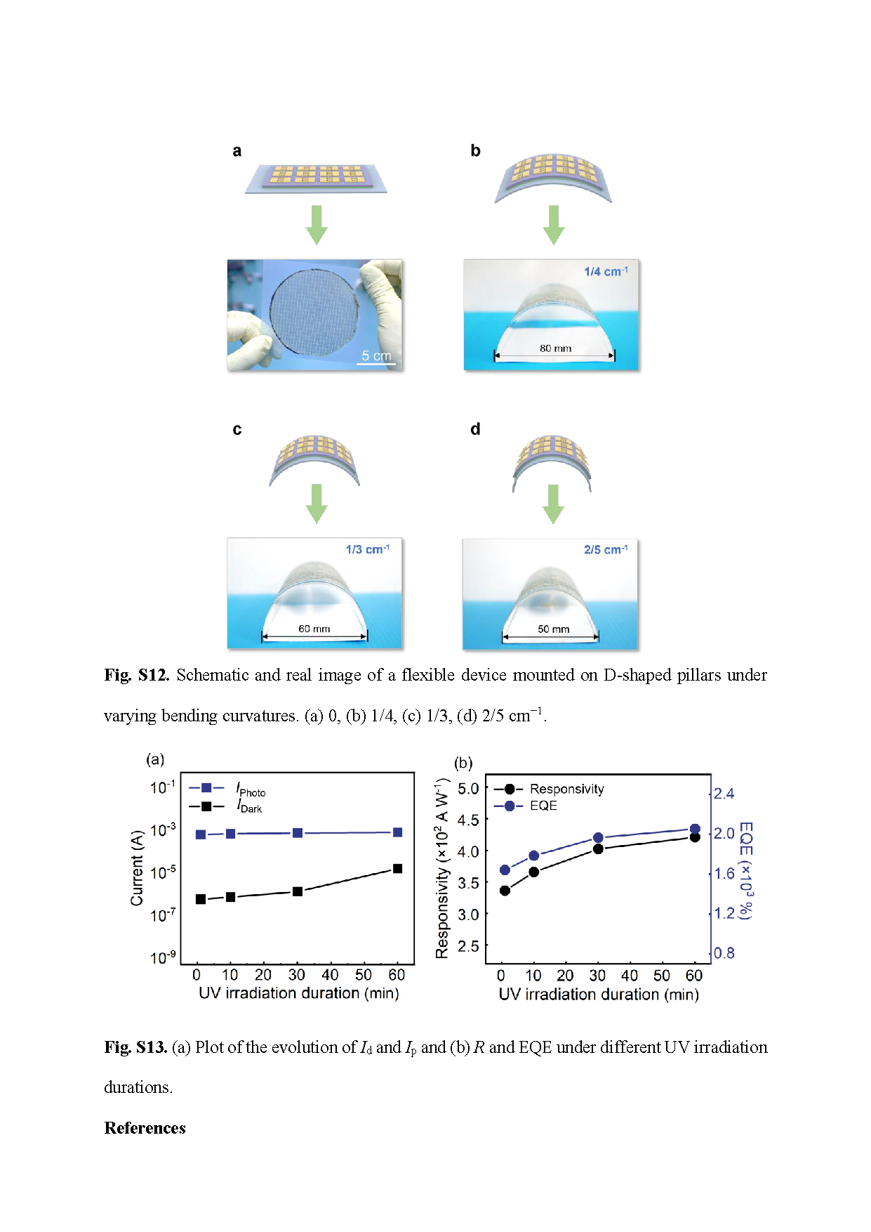
This study demonstrates the successful fabrication of a 4-inch wafer-scale flexible MSM UVPD based on a-Ga2O3. The a-Ga2O3 thin films are deposited via MOCVD, and a flexible device architecture is achieved through a combination of substrate removal and controlled film transfer. By employing an oxygen-rich growth strategy with an optimized oxygen flow rate of 1000 sccm, the concentration of Vo is effectively suppressed, leading to a reduced surface roughness of 0.73 nm and notable mitigation of the PPC effect. The resulting devices exhibited fast transient response times (τr/τd = 4.3/11.2 ms before transfer, 7.1/13.6 ms after transfer), along with consistent high performance across the transfer process, achieving average responsivities of 212.01 and 294.2 A W−1 and corresponding EQE of 1028.25 % and 1426.87 %. Furthermore, the devices maintained stable operation under repeated mechanical deformation and varying ultraviolet irradiation intensities, highlighting their excellent mechanical robustness, thermal reliability, and imaging capabilities. These findings establish a scalable and cost-effective pathway for the development of high-performance, large-area flexible a-Ga2O3-based UVPDs, offering strong potential for next-generation ultraviolet sensing and imaging systems.
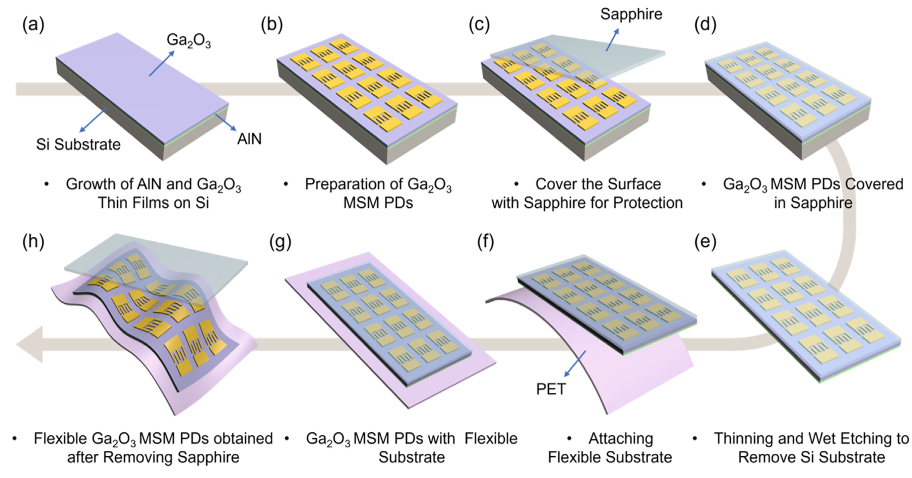
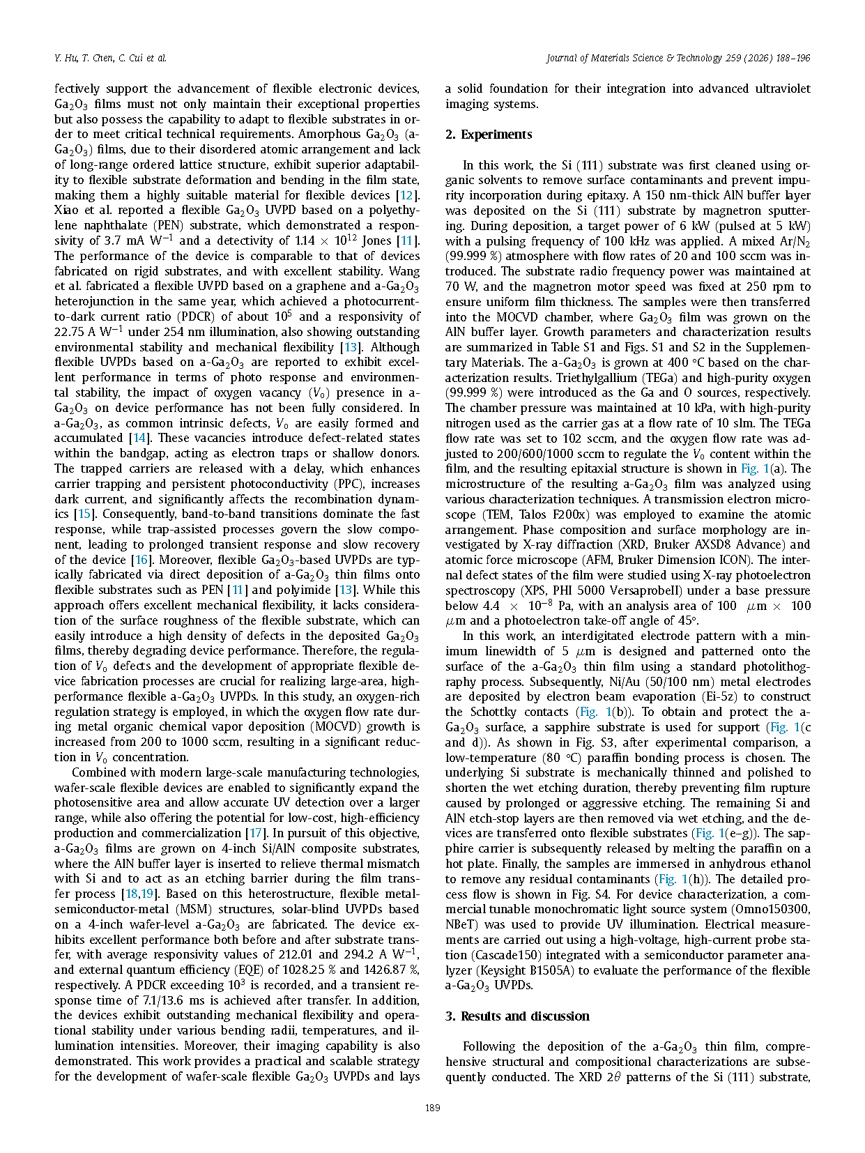
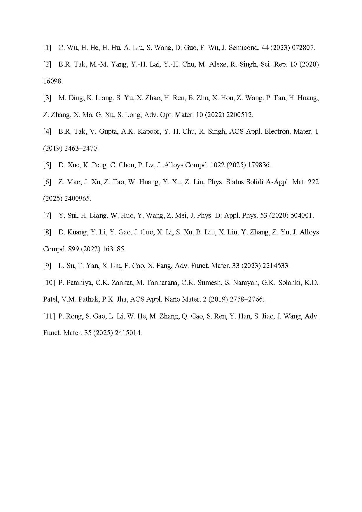
Fig. 1. The fabrication process of flexible MSM-structure a-Ga2O3 solar-blind UVPD.

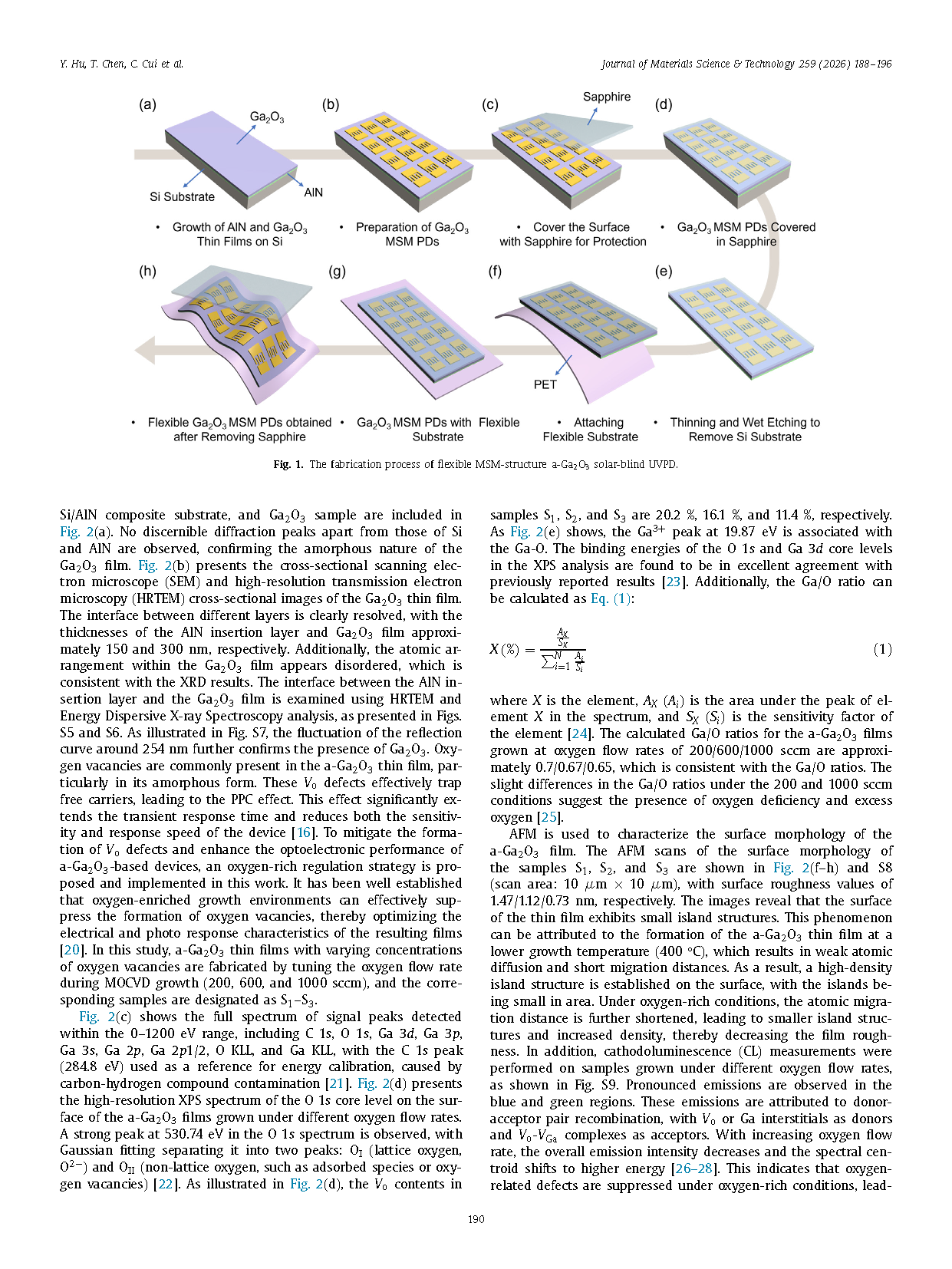
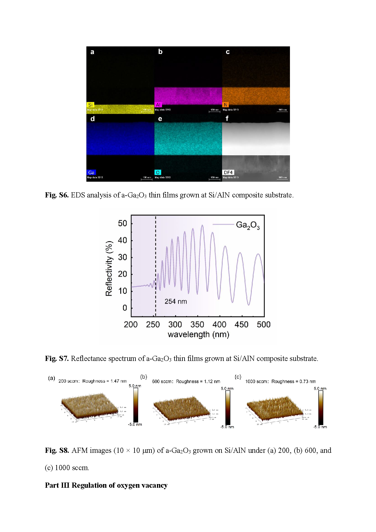
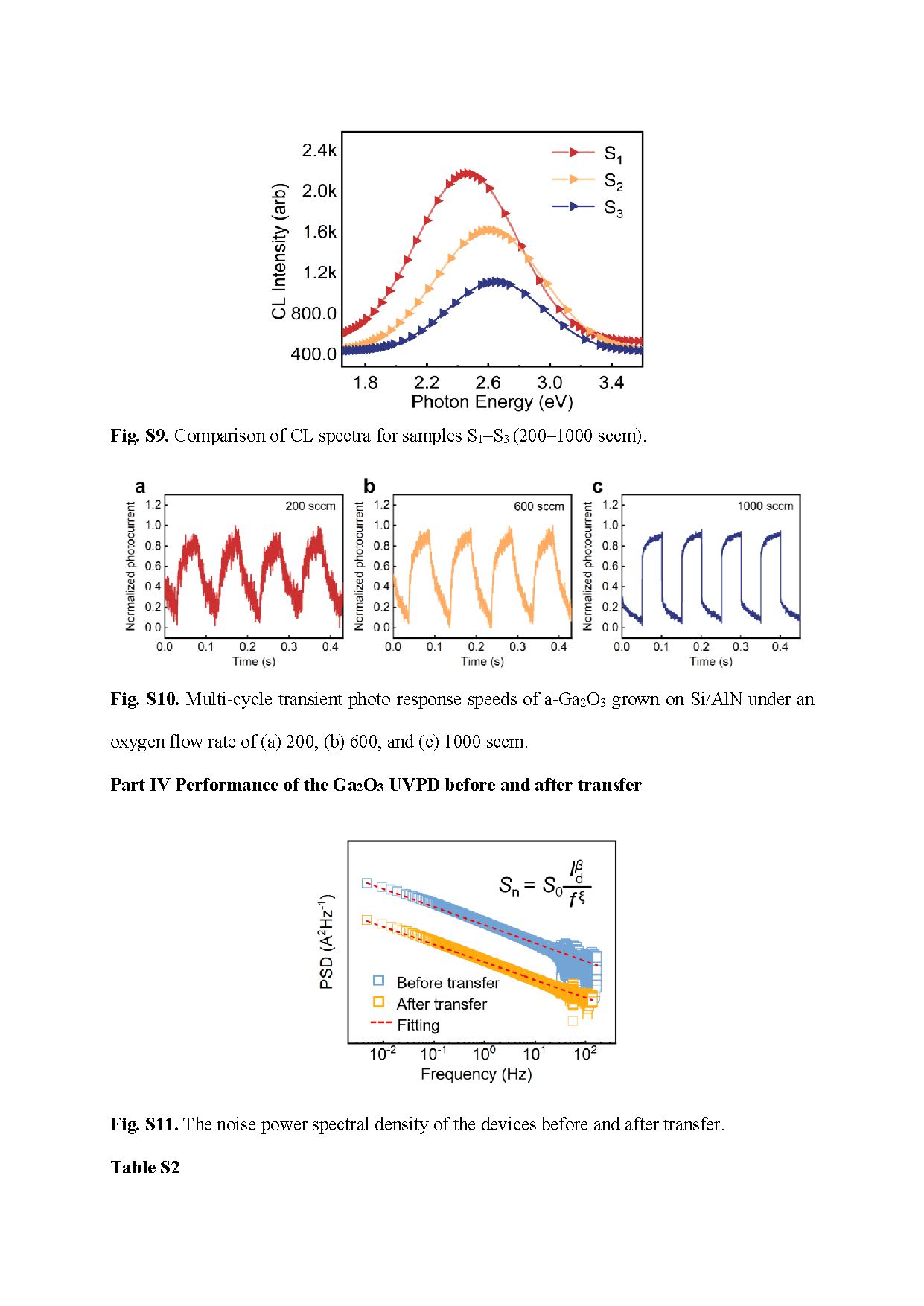
Fig. 2. (a) The 2θ XRD curves of the Si (111) substrate, Si/AlN composite substrate, and Ga2O3 sample. (b) SEM and HRTEM cross-sectional image at the interface between the AlN insertion layer and a-Ga2O3 film. (c) General XPS scan. (d) O 1s core level of a-Ga2O3 epitaxially. (e) Ga 3d core level of a-Ga2O3 epitaxially. AFM 3D images of a-Ga2O3 grown on Si/AlN under (f–h) 200, 600, and 1000 sccm.
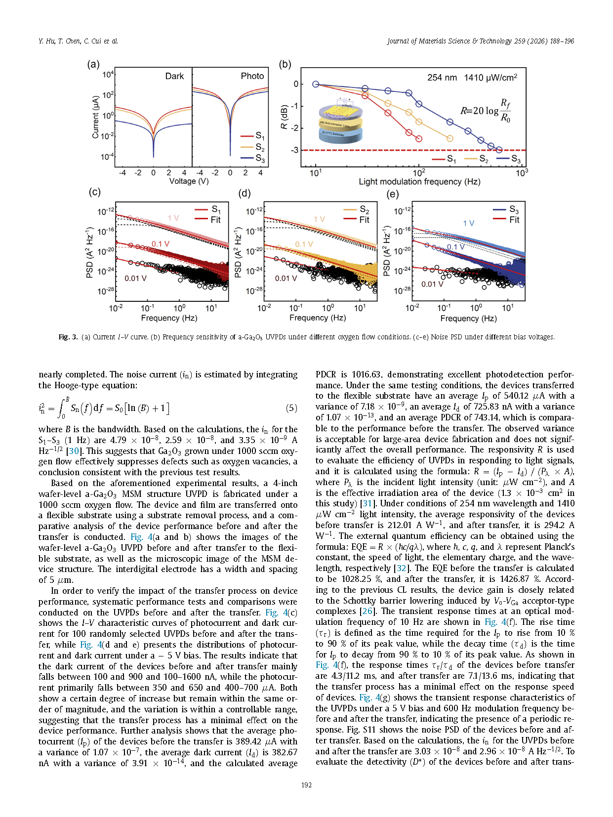
Fig. 3. (a) Current I –V curve. (b) Frequency sensitivity of a-Ga2O3 UVPDs under different oxygen flow conditions. (c–e) Noise PSD under different bias voltages.
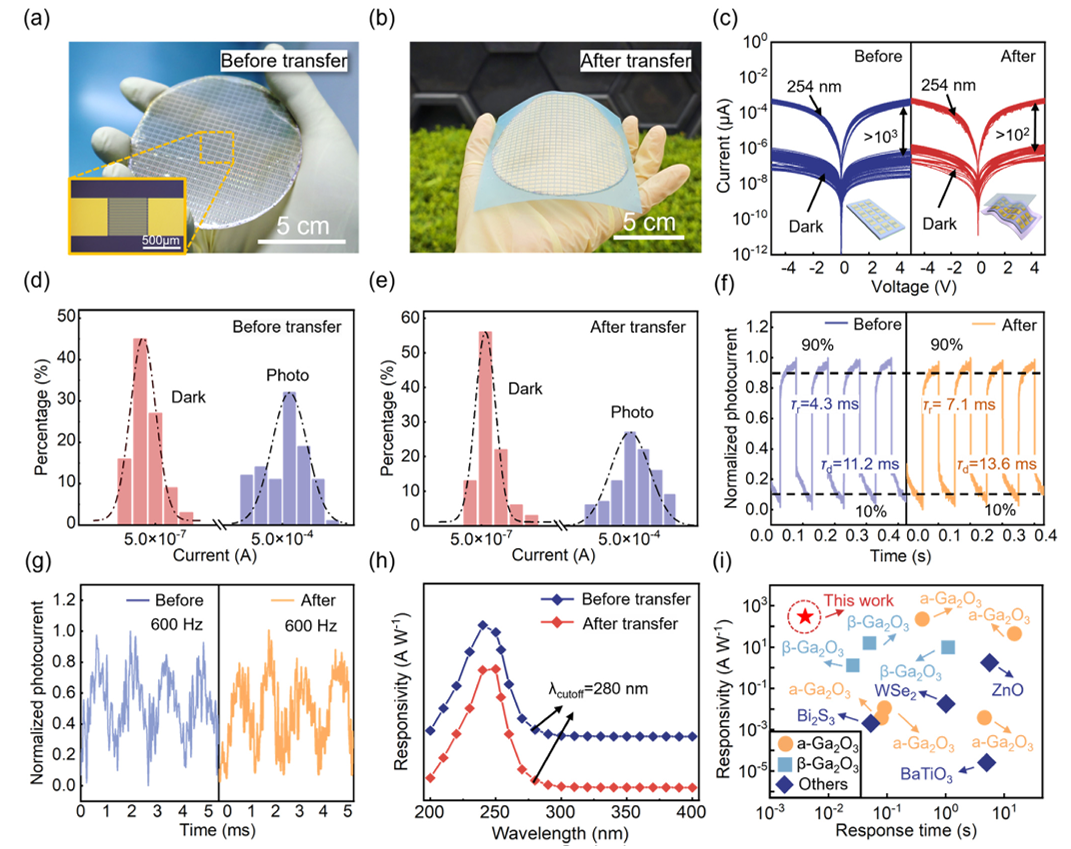
Fig. 4. (a and b) 4-inch flexible device before and after transfer. (c) I –V curves of 100 randomly selected UVPDs. (d and e) The distribution of dark and photocurrent values before and after device transfer of 100 randomly selected UVPDs. (f) The transient response times under 10 Hz modulation frequency. (g) The transient response characteristics at 600 Hz modulation frequency. (h) Response spectra in the range of 200–400 nm. (i) Comparison of UVPDs’ responsivity and response time with reported results.
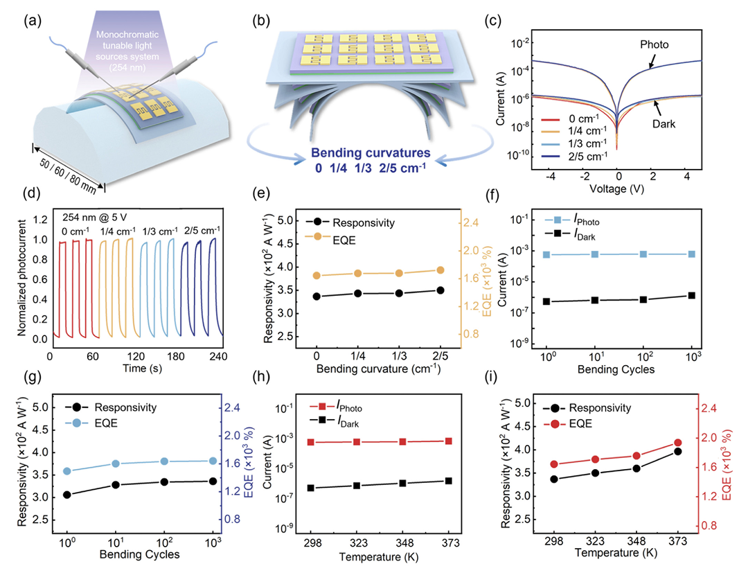
Fig. 5. Schematic diagram of (a) the D-shaped pillar bending test method and (b) flexible devices under different bending curvatures. (c) I –V curves of flexible devices under different bending curvatures. (d) Multi-cycle transient photo response. (e) R and EQE of flexible devices under different bending curvatures. (f) Plot of the evolution of Id and Ip versus bending cycle number. (g) R and EQE versus bending cycle number. (h) Plot of the evolution of Id and Ip under different work temperatures. (i) R and EQE under different work temperatures.
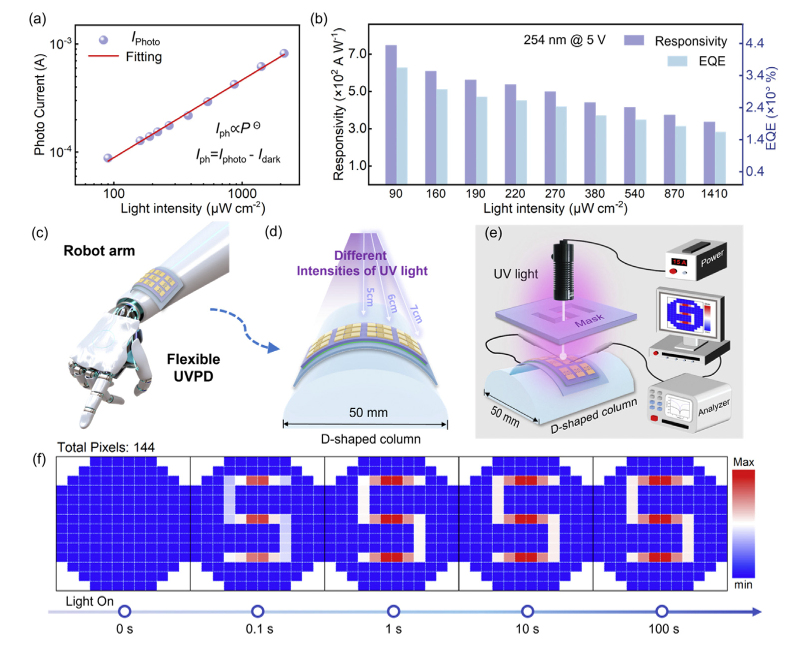
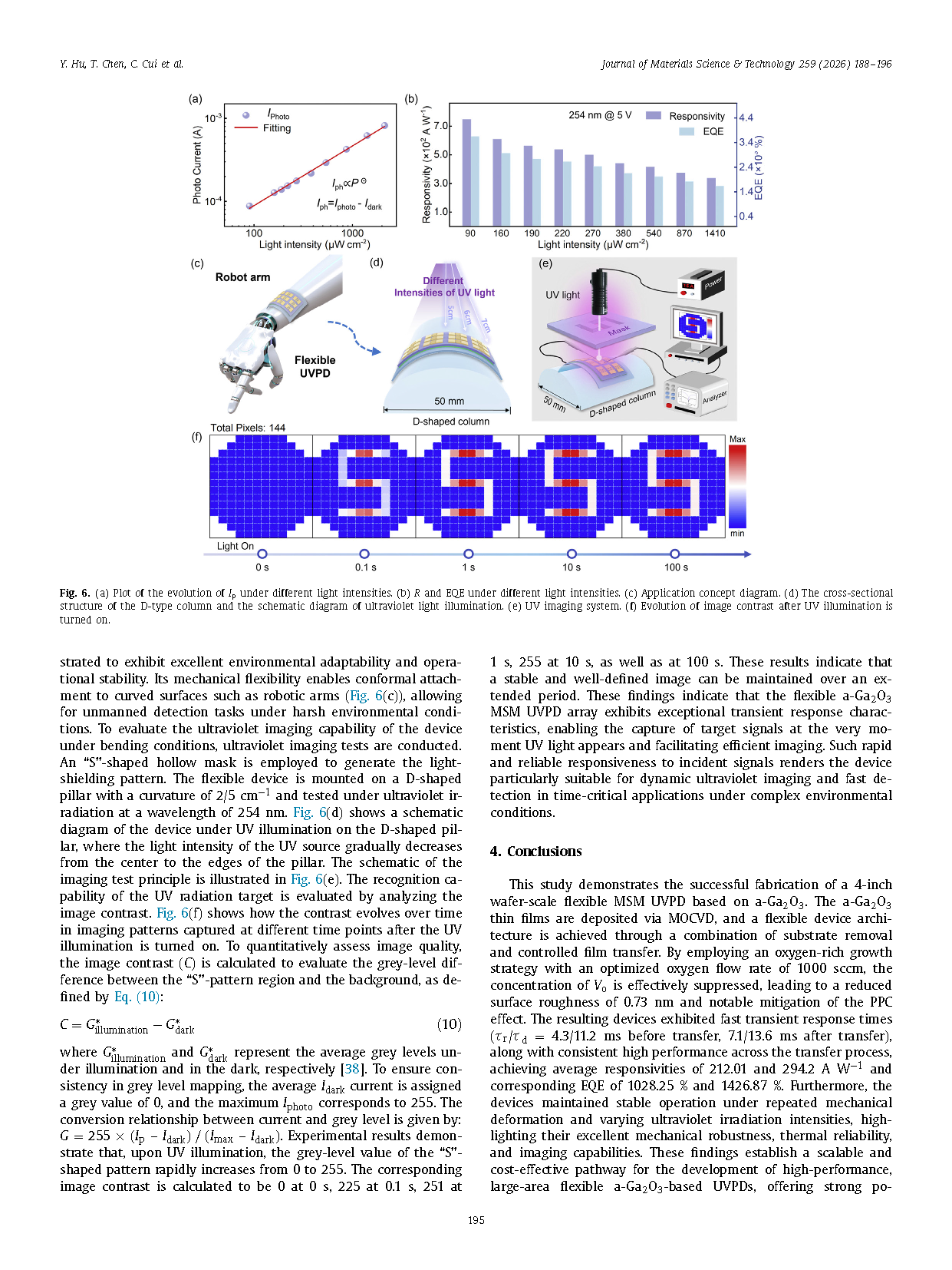
Fig. 6. (a) Plot of the evolution of Ip under different light intensities. (b) R and EQE under different light intensities. (c) Application concept diagram. (d) The cross-sectional structure of the D-type column and the schematic diagram of ultraviolet light illumination. (e) UV imaging system. (f) Evolution of image contrast after UV illumination is turned on.
DOI:
doi.org/10.1016/j.jmst.2025.10.005