


Member News
【Member News】GAREN SEMI Selected for the “Top 10 China Third-Generation Semiconductor Technology Achievements of 2025,” Leading the Global β-Ga₂O₃ Industry with Full-Chain Innovation
日期:2025-11-14阅读:840
On November 12, 2025, THE 11TH INTERNATIONAL FORUM ON WIDE BANDGAP SEMICONDUCTORS & THE 22ND CHINA INTERNATIONAL FORUM ON SOLID STATE LIGHTING (IFWS&SSLCHINA2025) grandly opened in Xiamen. At the meeting, Hangzhou GAREN SEMI Co., LTD. (hereinafter referred to as "GAREN SEMI") was successfully selected as one of the "Top Ten Advances in China's Third-Generation Semiconductor Technology in 2025" for its achievement of "Major Breakthrough in 8-inch Gallium Oxide Single Crystal and Substrate Preparation". This honor marks a crucial leap for our country in the field of ultra-wide band gap semiconductor materials, from "following" to "taking the lead", and further highlights the technical benchmark status of GAREN SEMI in the global Gallium Oxide industry.
Top 10 Advancements Fill the International Gap
The "Top 10 Advances in China's Third-Generation Semiconductor Technology in 2025" selection was initiated by the China Advanced Semiconductor Industry Innovation Alliance (CASA) and is one of the most authoritative and influential technical awards in the field of third-generation semiconductors in China. The selection process went through three stages: "43 valid achievements collection - 33 final TOP30 screening - strict review by the expert committee". The top ten advancements ultimately selected cover core fields such as Silicon Carbide, Gallium Nitride, and Gallium Oxide, all of which are breakthrough technologies that drive industrial upgrading.
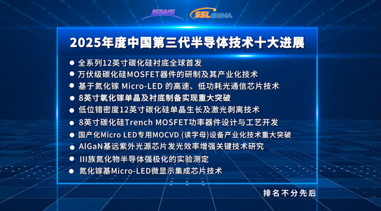
Figure 1 Top 10 Advancements in China's third-generation Semiconductor technology in 2025
Gallium Oxide, as a core material for ultra-wide band gap semiconductors, features a β-Ga₂O₃, as an ultra-wide bandgap semiconductor, possesses a bandgap of 4.85 eV and a high breakdown field of 8 MV/cm. It is a key fundamental material for the research and development of high-end power, RF and optoelectronic devices. However, traditional growth methods rely on a large amount of precious metals, are costly and incompatible with mainstream silicon-based production lines. Hangzhou GAREN SEMI Co., LTD., relying on its unique "casting method", has solved the problem of single crystal twin defect, broken through key technologies such as multi-physical field coupling control and controllable doping, built a thermal field system suitable for large-scale growth, achieved stable production, and has the advantages of low cost, high efficiency, and easy size expansion. Moreover, it has complete independent intellectual property rights. This achievement fills the gap in the international field of large-sized Gallium Oxide single crystal and substrates, support China's ultra-wide band gap semiconductors move from "following" to "taking the lead", and providing key material support for fields such as fast charging of new energy vehicles and smart grids.
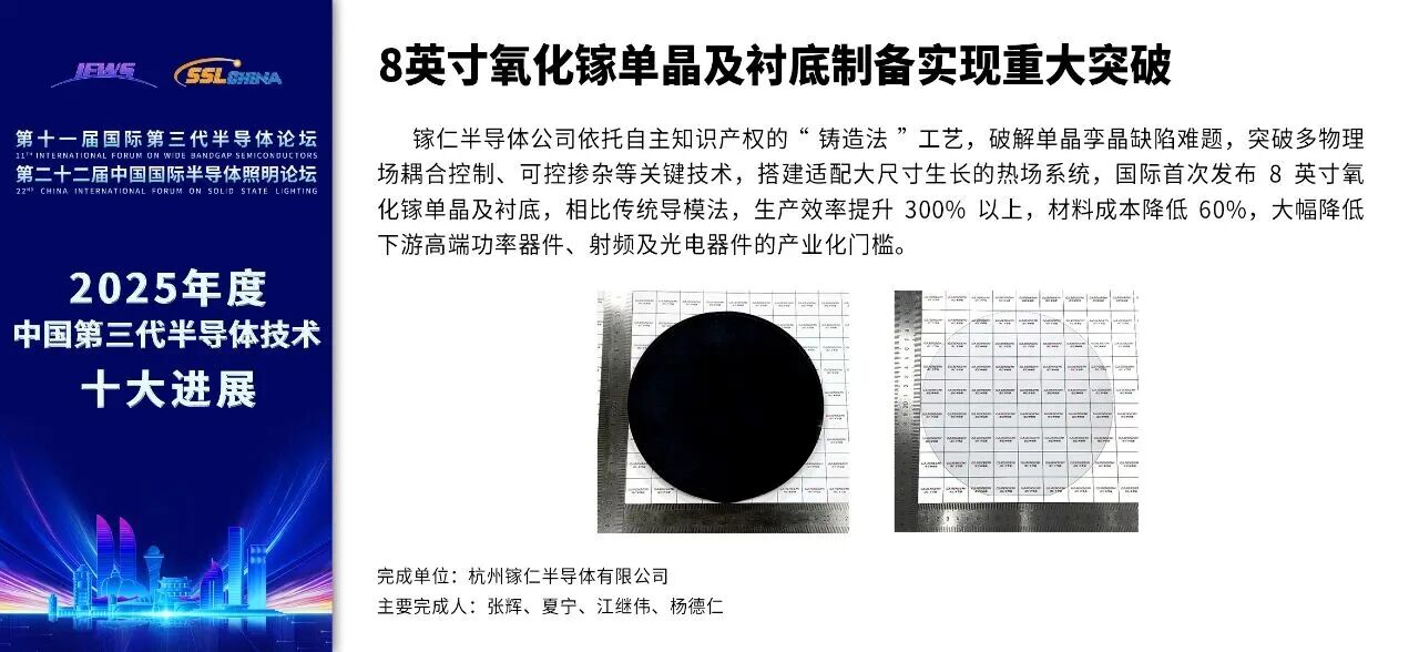
Figure 2 Selected achievements of GAREN SEMI
The Technology Explosion Sets Industry Records
2025 marks an "explosive year" for GAREN SEMI in terms of technological iteration and industrialization. The company has continuously achieved breakthroughs across three key dimensions—Gallium Oxide material size, crystal-plane technology, and equipment autonomy—reshaping the pace of industry development with its "Gallium speed".
In terms of size iteration, GAREN SEMI has achieved a leapfrog development from 2-inch to 8-inch Gallium Oxide substrates in just three years, setting an industry record of "iterating one size per year". In March 2025, the company globally launched an 8-inch Gallium Oxide single crystal and substrate, pushing the size of Gallium Oxide substrates to a new height and providing fundamental support for the research and development of large-sized devices downstream.
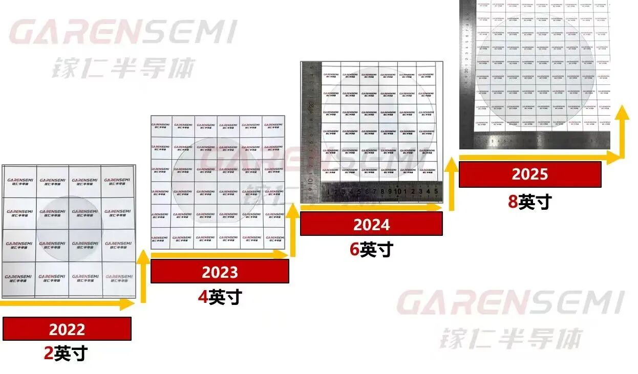
Figure 3 Size of GAREN SEMI Gallium Oxide substrate rapid evolution
In October of the same year, GAREN SEMI, relying on its independently developed dedicated equipment for the Vertical Bridgerman process (VB process), broke through the 6-inch (010) plane Gallium Oxide crystal growth technology. The length of the crystal ingot's equal diameter segment exceeded 40mm, reaching the international leading level and further enriching the large-sized Gallium Oxide product matrix.
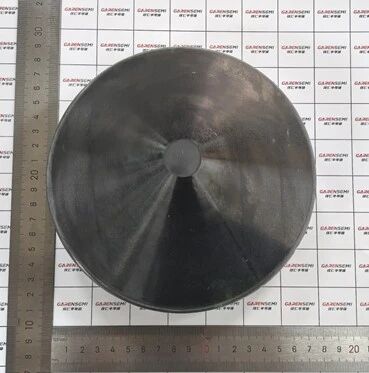
Figure 4 6-inch (010) plane Gallium Oxide ingot (conductive type) by GAREN SEMI VB method
In the field of crystal-plane technology, GAREN SEMI achieved multiple key breakthroughs in 2025. In February 2025, GAREN SEMI successfully fabricated a 6-inch chamfer Gallium Oxide substrate, with the main surface of the substrate being a (100) surface that was chamfer 4° along the [00-1] direction, providing crucial technical support for high-quality epitaxial growth.
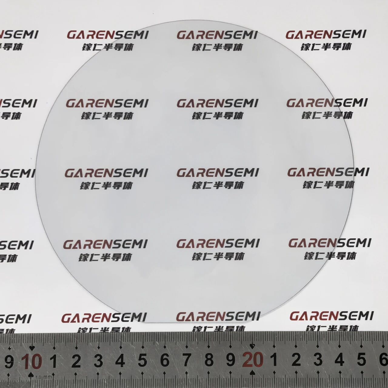
Figure 5 GAREN SEMI 6-inch chamfer Gallium Oxide substrate
In November of the same year, GAREN SEMI officially launched the new product (011) crystal face Gallium Oxide substrate. The performance test and surface quality maintained its consistently outstanding performance, providing a brand-new solution in the fields of epitaxial growth and device fabrication.
In terms of equipment autonomy, the company launched its self-developed VB method crystal growth equipment dedicated to Gallium Oxide in September 2024. In 2025, it will continue to optimize the equipment performance to achieve fully automated crystal growth, reduce manual intervention, and meet the strict requirements of Gallium Oxide growth for high-temperature and high-oxygen environments.
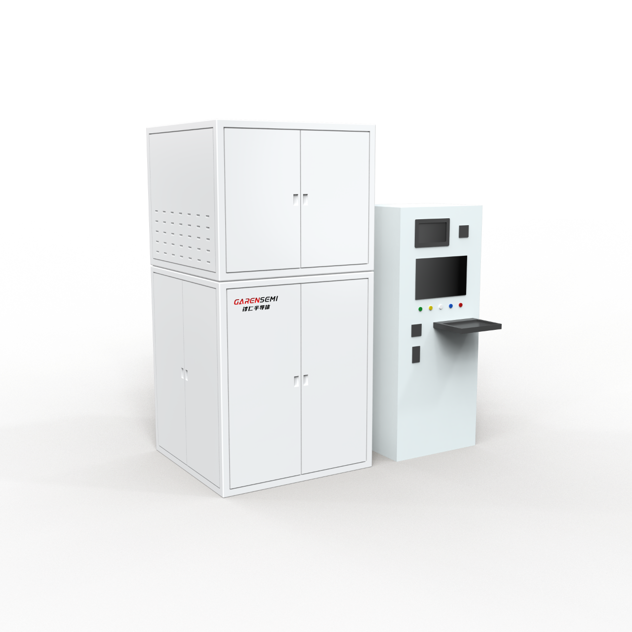
Figure 6 GAREN SEMI Gallium Oxide VB method specialized crystal growth equipment
This equipment not only can stably grow large-sized single crystal with various crystal face, but also supports upgrades to larger sizes. It has provided scientific research and production support for universities, research institutes and enterprise customers, and built an independent and controllable system covering the entire chain of "equipment - process - materials".
Honored and Driving Industry Advancement
In 2025, GAREN SEMI won multiple authoritative honors for its technological breakthroughs and industrial contributions in the field of Gallium Oxide, and continued to lead the upgrading of the Gallium Oxide industry.
In addition to being named one of the “Top Ten Advances in China’s Third-Generation Semiconductor Technology in 2025,” the company kicked off its “honor-harvesting mode” at the start of the year:
In March 2025, GAREN SEMI was awarded the "SEMI Outstanding Contribution Award for Sustainable Development" at SEMICON CHINA, the world's largest semiconductor industry event, highlighting the concept of green production.
In April 2025, GAREN SEMI won the " Solidarity Colleagues Award" at the 2025 Jiufengshan Conforence (JFSC), demonstrating the value of industrial chain collaboration.
In May 2025, GAREN SEMI was awarded the "Innovation Vitality Award" in the semiconductor industry of Zhejiang Province for its technological innovation capabilities, becoming a benchmark in the local semiconductor industry.
In September 2025, GAREN SEMI represented the Hangzhou region and won the second prize in the enterprise group of the 10th "Maker China" Zhejiang Provincial Finals, demonstrating its outstanding technological innovation capabilities and industrialization achievements.
In October 2025, GAREN SEMI achieved a double celebration - not only did it successfully enter the top 500 of the national enterprise group in the 10th "Maker China" Small and Medium-sized Enterprises Innovation and Entrepreneurship Competition, but it also shared the "2024-2025 Semiconductor Materials Industry Contribution Award" with four leading enterprises in the domestic semiconductor materials field.
Behind a series of honors lies the continuous and in-depth empowerment of the Gallium Oxide industry by GAREN SEMI.
At present, the company has established a complete technical system covering Gallium Oxide single crystal growth, substrate preparation, homogeneous epitaxy and the research and development of dedicated equipment. Its products not only supply the domestic market but also attract the attention of international customers, continuously promoting the localization process of ultra-wide band gap semiconductor materials in China.
In the future, GAREN SEMI will continue to focus on the Gallium Oxide field, making efforts in the research and development and industrial application of larger-sized and higher-quality materials, and support China occupy a core position in the global ultra-wide band gap semiconductor industry competition, injecting core power into the development of strategic industries such as new energy, 5G, and smart grids!
For more information about GAREN SEMI and its products
Visit our official website: http://garen.cc/
Or contact us in the following ways:
Mr. Jiang :15918719807
Email :jiangjiwei@garen.cc
Mr. Xia :19011278792
Email :xianing@garen.cc
