


Paper Sharing
【Member Papers】Multiband bipolar photoresponse in Cu@CuOₓ@a-Ga₂O₃ core-shell heterostructure-based self-powered photoelectrochemical-type photodetector for secure underwater optical communication
日期:2025-11-13阅读:419
Abstract
Photoelectrochemical-type bipolar photodetectors (PEC-BPDs), featuring wavelength-dependent, polarity-switchable photoresponse, hold great promise for the development of secure, multi-channel, and energy-efficient underwater optical communication systems. Here, a self-powered PEC-BPD is constructed based on a vertically aligned Cu@CuOx@a-Ga2O3 core-shell heterostructure, achieving broadband photodetection spanning from deep ultraviolet (UV) to near-infrared (NIR) wavelengths, along with reversible photocurrent polarity switching. By precisely modulating the transport dynamics of photogenerated charge carriers, the underlying mechanism of wavelength-induced current inversion is elucidated, enabling bipolar responses under multiband light excitation (UV-UV, UV–visible, and UV-NIR). Leveraging this multiband dual-polarity behavior, multiple reconfigurable logic operations (OR, NOT, XOR, NAND) are realized within a single PEC-BPD. Furthermore, by incorporating alternate mark inversion encoding, the system achieves encrypted underwater optical communication in the spectral dimension with parallel data transmission and intrinsic error-correction capability. This work offers a novel strategy for multifunctional optoelectronic device design and opens new avenues toward next-generation intelligent and secure underwater optical communication systems based on PEC-BPDs.
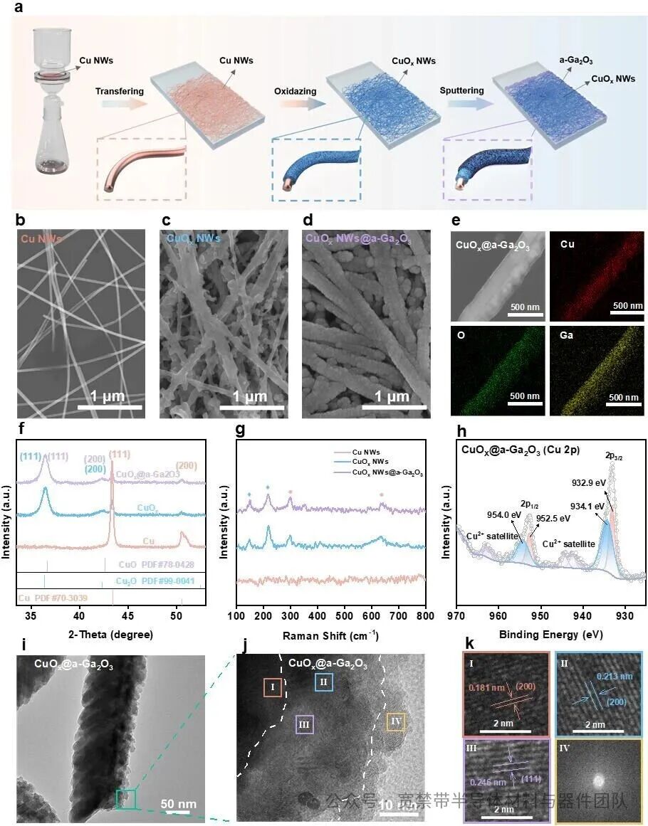
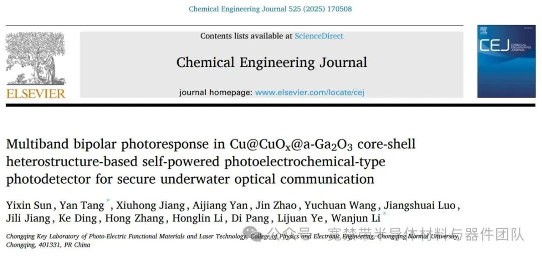
Figure 1. Preparation and characterization of Cu@CuOx@a-Ga2O3 network films. a) Schematic illustration of the preparation process for Cu@CuOx@a-Ga2O3 network films. SEM images of Cu NWs networks b), Cu@CuOx network film c), and Cu@CuOx@a-Ga2O3 network film d). e) SEM image combined EDS elemental mapping of a single Cu@CuOx@a-Ga2O3 nanowire. f) XRD spectrum, g) Raman scattering spectrum of Cu NWs film, Cu@CuOx film and Cu@CuOx@a-Ga2O3 film. h) Cu 2p XPS spectrum of Cu@CuOx@a-Ga2O3. i) TEM image of Cu@CuOx@a-Ga2O3. j) HRTEM image of the green boxed area in (i). k) The magnified regions (I-III) and FFT image (IV) of the corresponding color boxed areas in (i).
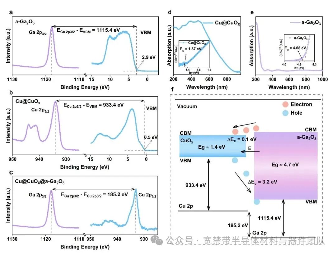
Figure 2. Energy band structure of CuOx@a-Ga2O3. a) Ga 2p3/2 core-level spectrum and valence band spectrum of a-Ga2O3. b) Cu 2p3/2 core-level spectrum and valence band spectrum of Cu@CuOx. c) Ga 2p3/2 and Cu 2p3/2 core-level spectra of Cu@CuOx@a-Ga2O3. d) Absorption spectrum and optical band gap of Cu@CuOx. e) Absorption spectrum and optical band gap of a-Ga2O3. f) Schematic illustration of the energy band alignment of CuOx@a-Ga2O3 in the working electrode.
Figure 3. Investigation on the wavelength-induced bipolar mechanism of Cu@CuOx@a-Ga2O3 PEC-BPDs with varying a-Ga2O3 layer thickness. a) Broad-spectrum photoelectric properties of a-Ga2O3 and Cu@CuOx PEC-PDs (0 V, 0.8 mW/cm2). b) Broad-spectrum photoelectric properties of Cu@CuOx@a-Ga2O3 PEC-BPD (0 V, 0.8 mW/cm2). c) I-t curves under 254 nm light irradiation and d) I-t curves under 365 nm light irradiation of Cu@CuOx@a-Ga2O3 PEC-BPDs with different a-Ga2O3 deposition times (0 V, 0.8 mW/cm2). Band bending and charge transfer under 254 nm light irradiation for Cu@CuOx@a-Ga2O3 films with thin e), medium f), and thick g) a-Ga2O3 layers. Band bending and charge transfer under 365 nm light irradiation for Cu@CuOx@a-Ga2O3 films with thin h), medium i), and thick j) a-Ga2O3 layers.
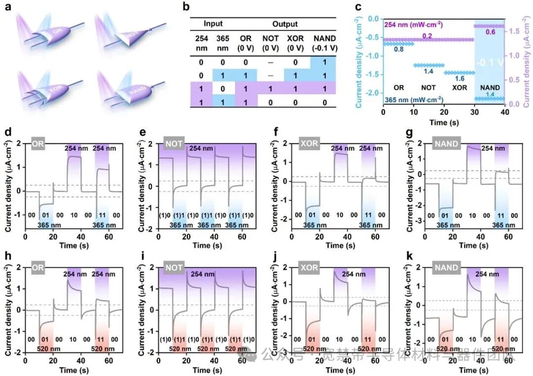
Figure 4. Demonstration of reprogrammable optical switching logic gates based on Cu@CuOx@a-Ga2O3 PEC-BPD with 30 min a-Ga2O3 sputtering time. a) Schematic diagrams of four optical switching logic gates: OR, NOT, XOR, and NAND. b) Truth table of OR, NOT, XOR, and NAND logic gates. c) Photocurrent values of Cu@CuOx@a-Ga2O3 PEC-BPD by single input signals (254 or 365 nm) for different logic gates, with the light intensity and bias voltage of the two signals. I-t curves of OR d), NOT e), XOR f), and NAND g) logic gates with 254 nm and 365 nm illumination. I-t curves of OR h), NOT i), XOR j), and NAND k) logic gates with 254 nm and 520 nm illumination. The on/off states of 254 nm and 365 nm/520 nm LEDs correspond to input logic states of 1/0. For the output photocurrent within the range of -0.25~0.25 μA/cm2, the output state is set as “0”, while the photocurrent outside this range indicates the output state “1”.

Figure 5. Demonstration of the encrypted optical communication system. a) Conceptual diagram of encrypted optical communication system. b) Diagram of AMI code splitting. c) The self-verification mechanism of the system when abnormal signal occurs. The bipolar photocurrent response curves of the Cu@CuOx@a-Ga2O3 PEC-BPD under parallel signal transmission with combined wavelengths of 254 nm and 365 nm d), 254 nm and 520 nm e) to transmitte the information “CQNU”.
DOI:
https://doi.org/10.1016/j.cej.2025.170508
