Paper Sharing
【International Papers】Heteroepitaxial Growth of β-Ga₂O₃ on Diamond (111) via Radio Frequency Magnetron Sputtering: Mechanistic Insights from Scanning/Transmission Electron Microscopy
日期:2025-11-13阅读:435
Researchers from the Kyushu University have published a dissertation titled "Heteroepitaxial Growth of β-Ga2O3 on Diamond (111) via Radio Frequency Magnetron Sputtering: Mechanistic Insights from Scanning/Transmission Electron Microscopy" in Small.
Background
In recent years, a significant body of research has been dedicated to investigating the prospective utilization of β-Ga2O3 in next-generation power electronics and sensing devices. The material's noteworthy physical properties include a wide bandgap of 4.5–4.9 eV, a high breakdown electric field (≈8 MV cm−1), profound chemical stability, and radiation resistance. Furthermore, the reduced manufacturing cost of β-Ga2O3 single-crystal wafers renders it a more cost-effective alternative to commercially viable power device materials, such as SiC and GaN. Notwithstanding the potential material properties of β-Ga2O3, which are excellent, its practical deployment is constrained by two factors. First, the material's low thermal conductivity (10–30 W m−1 K−1) poses a significant challenge. Second, the material's inability to achieve p-type electrical conductivity due to hole self-trapping limits its applications to unipolar devices.
Abstract
This study delves into the comprehensive microstructural analysis of heteroepitaxial β-Ga2O3 thin films grown on single-crystal diamond (111) wafers by radio frequency magnetron sputtering. The heterostructure is probed through a scanning/transmission electron microscope and succeeded in direct observation of β-Ga2O3 <010>||diamond [1-10] and β-Ga2O3 <132>||diamond [1-10] heteroepitaxial interfaces, which up to now have only has been inferred through indirect analyzing methods based on X-ray diffraction. Fast Fourier Transformation (FFT) patterns of corresponding oriented interfaces exhibited virtual overlapping for the substrate and the epilayer, authenticating the robust epitaxial arrangement. Furthermore, this study elucidates the discrete growth modes of β-Ga2O3 <010> and <132> domains arising from the asymmetric hexagonal C─O lattice matching, through 4D-STEM analysis and subsequent virtual dark-field image reconstruction. Strategies for the improvement of crystallinity, surface morphology, and facile thickness controllability of the β-Ga2O3 epilayer through optimizing the RF power, facilitating a low re-evaporation rate of the film, are discussed. This finding underscores the importance of domain control in the improved epitaxial quality of β-Ga2O3 that can inform the development of budget-friendly and scalable β-Ga2O3/diamond heterostructures for advanced functional devices.
Conclusion
In summary, this study succeeded in direct observation of the heteroepitaxial interface of β-Ga2O3/diamond (111) heterostructure fabricated by RFMS for the first time. The HR-TEM and ADF-STEM images, at the β-Ga2O3/diamond (111) interface have confirmed β-Ga2O3<010>||diamond [1-10] and β-Ga2O3<132>||diamond [1-10] epitaxial arrangements. In the atomic resolution S/TEM observation of grain boundaries in the β-Ga2O3 crystal, it was perceived that the β-Ga2O3 <010> domains restrain from forming twin grain boundaries in contrast with β-Ga2O3 <132> domains, suggesting different growth modes of the concerned domains. In 4D-STEM measurements and subsequent large area VDF reconstruction, the β-Ga2O3 <010> domain showed a preferential 3D growth mode characterized by columnar crystal grains, whereas the β-Ga2O3 <132> domain demonstrated a horizontally 2D growth mode. 2D growth is generally considered beneficial for thin film growth at the single-crystal level. Therefore, it has been demonstrated that the control of the growth domains is a pivotal factor in determining the caliber of β-Ga2O3 thin films. This study offers insights into the production of low-cost and high-quality β-Ga2O3/diamond heterostructures by RFMS for active thermal management and advanced bipolar power rectifiers. The authors, in their coming reports, will strive to achieve domain control by optimizing the RFMS growth parameters and substrate off-angles.
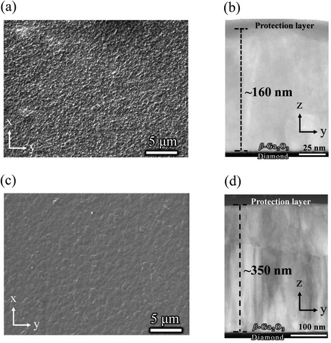
Figure 1. The high magnification SEM image of the β-Ga2O3 film surface fabricated at a) 50 W and c) 35 W. The cross-sectional ADF-STEM image of β-Ga2O3 film fabricated at b) 50 W and d) 35 W.
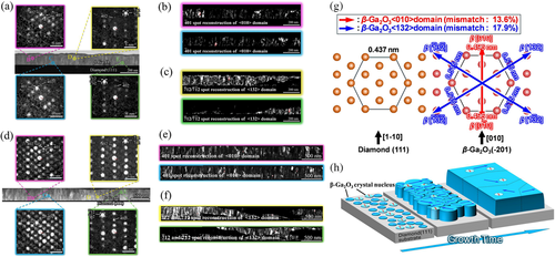
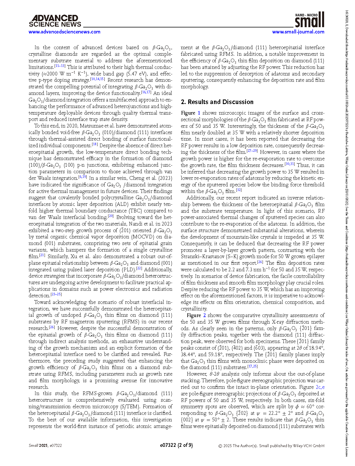
Figure 2. a) θ-2θ XRD scans of β-Ga2O3/diamond (111) heterostructures fabricated at 50 and 35 W. b) XRD rocking curves of β-Ga2O3 (2̅01) peak of respective samples. X-ray pole figure stereographic projections of β-Ga2O3/diamond (111) heterostructures fabricated at c) 50 W e) 35 W, and their corresponding rotational intensity mapping d,f) at ψ = 50°. g) XPS wide spectrum and Ga 3d narrow spectrum of a 35 W grown β-Ga2O3 film.
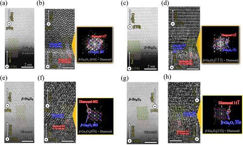
Figure 2. a) θ-2θ XRD scans of β-Ga2O3/diamond (111) heterostructures fabricated at 50 and 35 W. b) XRD rocking curves of β-Ga2O3 (2̅01) peak of respective samples. X-ray pole figure stereographic projections of β-Ga2O3/diamond (111) heterostructures fabricated at c) 50 W e) 35 W, and their corresponding rotational intensity mapping d,f) at ψ = 50°. g) XPS wide spectrum and Ga 3d narrow spectrum of a 35 W grown β-Ga2O3 film.
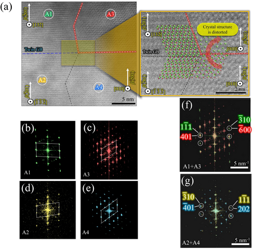
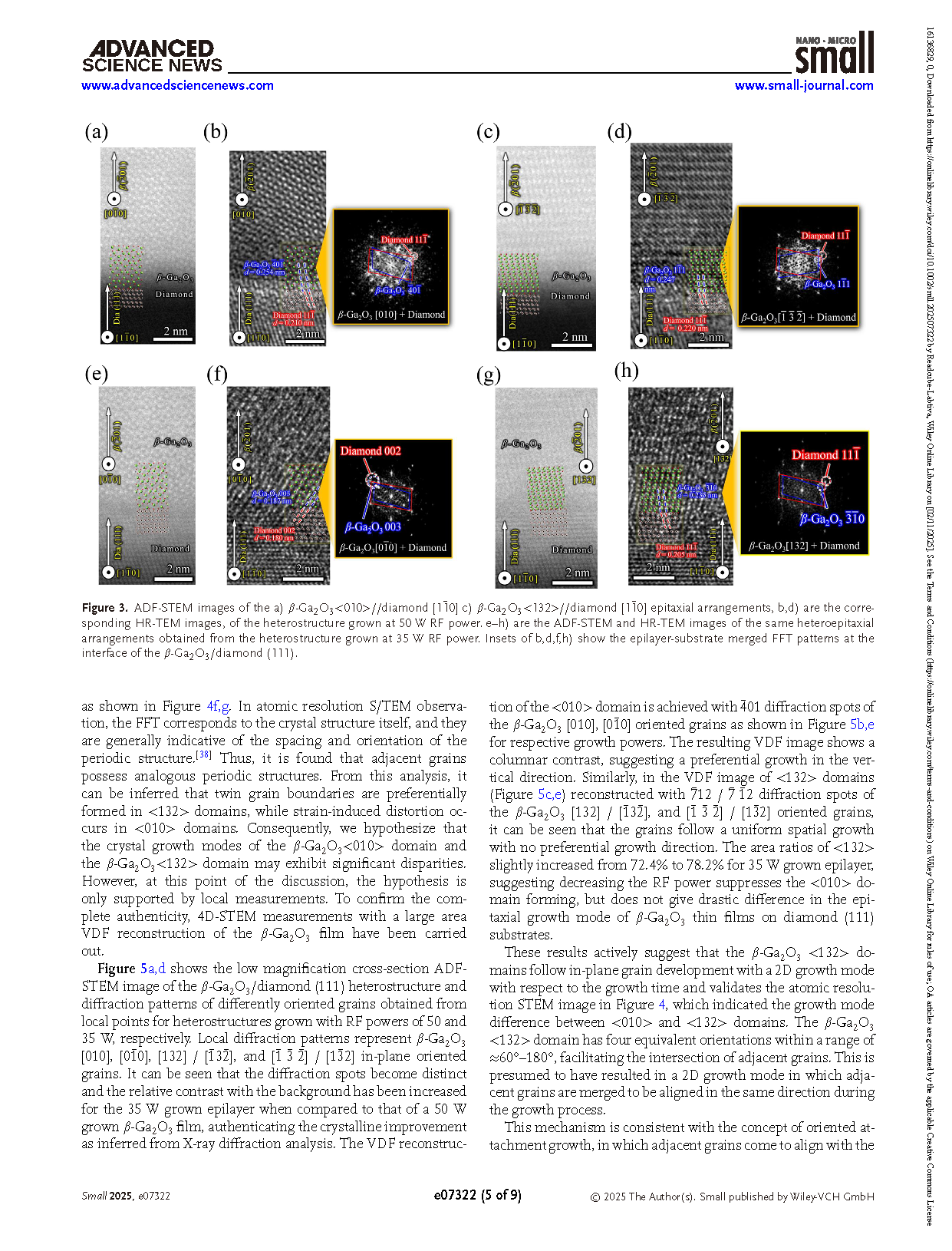
Figure 4. a) Cross-section ADF-STEM image of β-Ga2O3 film at a grain boundary. b–e) are the FFT patterns of areas A1, A2, A3, and A4 marked in (a), respectively. f,g) are the merged FFT patterns of selected areas.
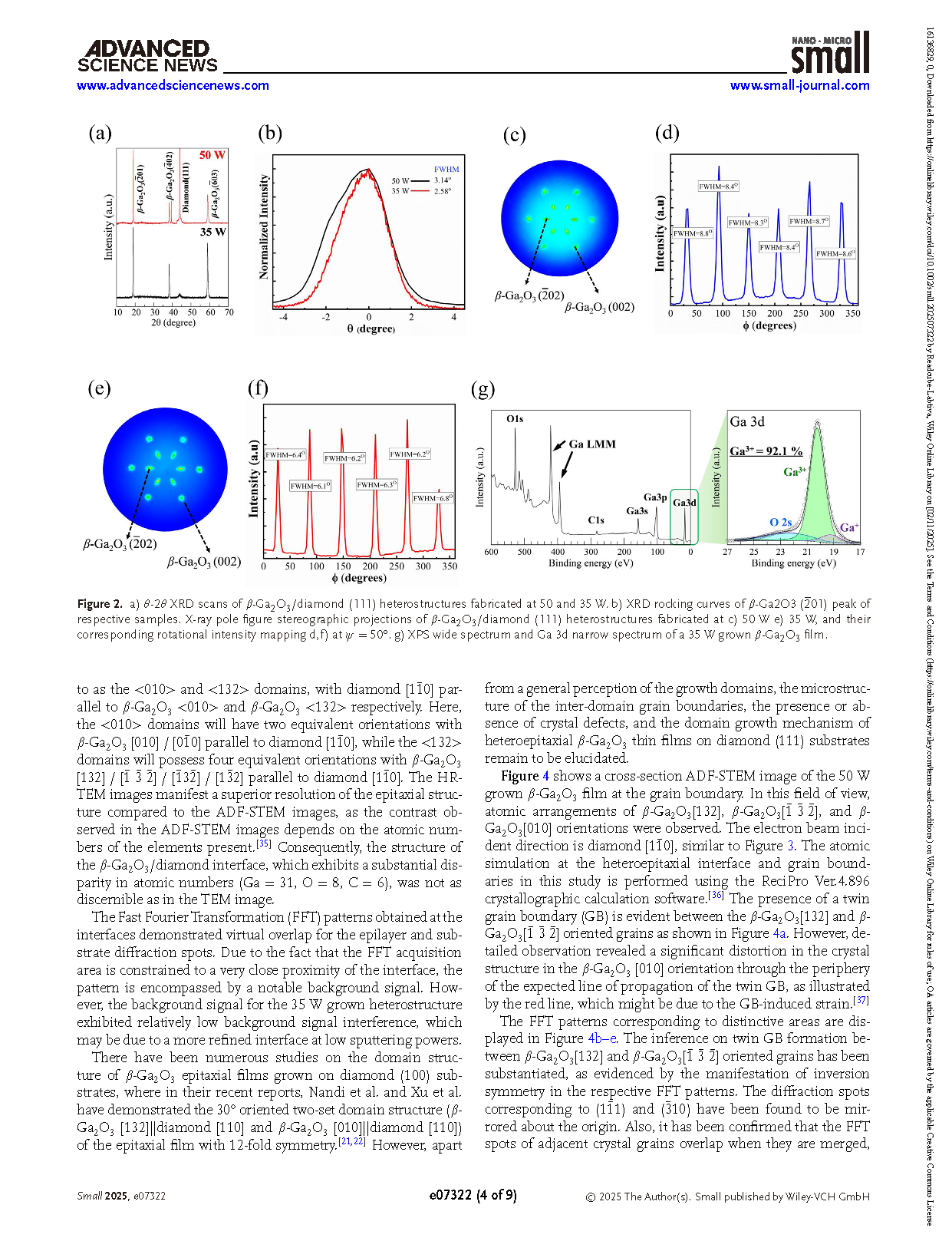
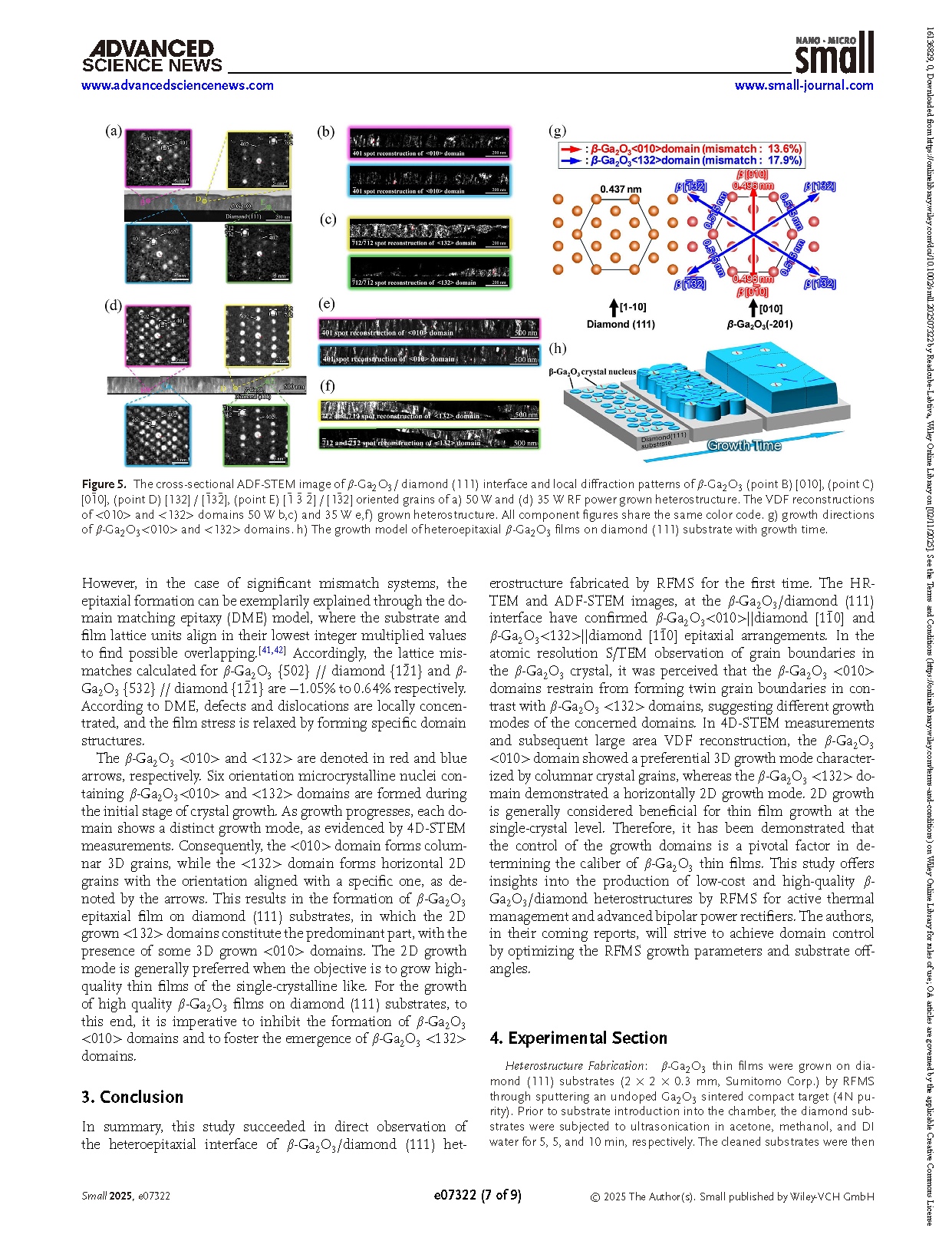
Figure 5. The cross-sectional ADF-STEM image of β-Ga2O3/ diamond (111) interface and local diffraction patterns of β-Ga2O3 (point B) [010], (point C) [0-10], (point D) [132] / [-13-2], (point E) [-1-3-2] / [1-32] oriented grains of a) 50 W and (d) 35 W RF power grown heterostructure. The VDF reconstructions of <010> and <132> domains 50 W b,c) and 35 W e,f) grown heterostructure. All component figures share the same color code. g) growth directions of β-Ga2O3<010> and <132> domains. h) The growth model of heteroepitaxial β-Ga2O3 films on diamond (111) substrate with growth time.
DOI:
doi.org/10.1002/smll.202507322