Paper Sharing
【Member Papers】 (100) Microcracks induced by (1 ± 11) stacking faults in halide vapor deposited (001) β-Ga₂O₃: Origin of reverse leakage current in Schottky barrier diodes observed by high-sensitive emission microscopy and synchrotron x-ray topography
日期:2025-11-12阅读:423
Researchers from the Saga University and Novel Crystal Technology have published a dissertation titled "(100) Microcracks induced by (1 ± 11) stacking faults in halide vapor deposited (001) β-Ga2O3: Origin of reverse leakage current in Schottky barrier diodes observed by high-sensitive emission microscopy and synchrotron x-ray topography " in Journal of Applied Physics.
Background
This study focuses on β-Ga₂O₃, an ultra-wide bandgap semiconductor with a bandgap of 4.8 eV and a high breakdown field of 8 MV/cm, making it a promising candidate for high-power and high-efficiency electronic devices. N-type β-Ga₂O₃ can be achieved through Si or Sn doping, and high-performance Schottky barrier diodes (SBDs) have been demonstrated with breakdown voltages up to 2.89 kV and low on-resistance values. These devices typically utilize β-Ga₂O₃ epitaxial layers grown by the halide vapor phase epitaxy (HVPE) technique, which enables high growth rates and high-quality thick drift layers suitable for vertical power devices.
However, despite these advantages, SBDs often suffer from high reverse leakage current and reduced breakdown voltage due to so-called “killer defects,” whose origins remain unclear. Various types of defects have been reported in β-Ga₂O₃, including voids, polycrystalline regions, stacking faults, dislocations, and microgrooves. Building upon these findings, this study identifies microcracks induced by stacking faults in HVPE-grown (001) β-Ga₂O₃ epitaxial layers for the first time. The research further reveals the facet planes and associated dislocation networks around these microcracks, demonstrating that such stacking-fault-induced microcracks act as critical killer defects responsible for the reverse leakage behavior in HVPE-grown β-Ga₂O₃ SBDs.
Abstract
This study reports that microcracks on a halide vapor-phase epitaxy (HVPE)-deposited (001) β-Ga2O3 epitaxial layer are killer defects in Schottky barrier diodes (SBDs). The microcracks are (100) cracks with a typical length of 1.7–5.1 μm and depth of 0.48–2.2 μm. They are accompanied by (111) or (1-11) stacking faults and dislocation networks, causing a large reverse-leakage-current flow in SBDs. The stacking faults were generated during HVPE growth. The microcracks were considered to be formed by tensile strain caused by the difference in thermal expansion coefficients between the [100] and [010] directions during growth, annealing, etc. The electric field at the bottom of the microcrack was 6.0 MV/cm at −80 V, which resulted in a reverse leakage current in the SBD.
Conclusion
In this paper, we found that microcracks on an HVPE (001) β-Ga2O3 epitaxial layer grown on an EFG (001) β-Ga2O3 substrate were killer defects in SBDs. The microcracks were (100) cracks with a typical length of 1.7–5.1 μm and depth of 0.48–2.2 μm. They were induced by stacking faults and cause reverse leakage current paths [896 nA (8.87 μA/cm2) at −80 V]. The stacking faults were (1±11) facets. This indicates that they occurred during HVPE growth. Subsequently formed dislocation networks were observed around microcracks and stacking faults.
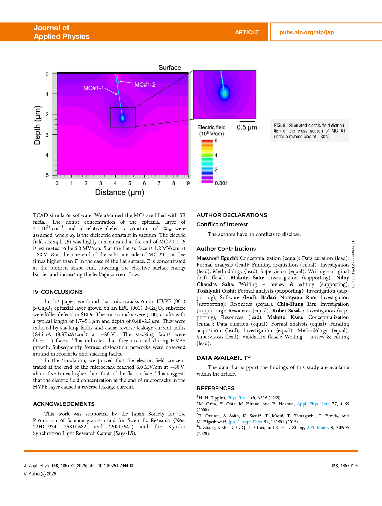
In the simulation, we proved that the electric field concentrated at the end of the microcrack reached 6.0 MV/cm at −80 V, about five times higher than that of the flat surface. This suggests that the electric field concentration at the end of microcracks in the HVPE layer caused a reverse leakage current.
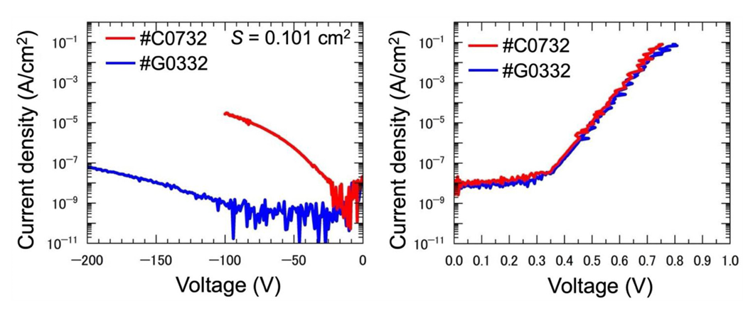
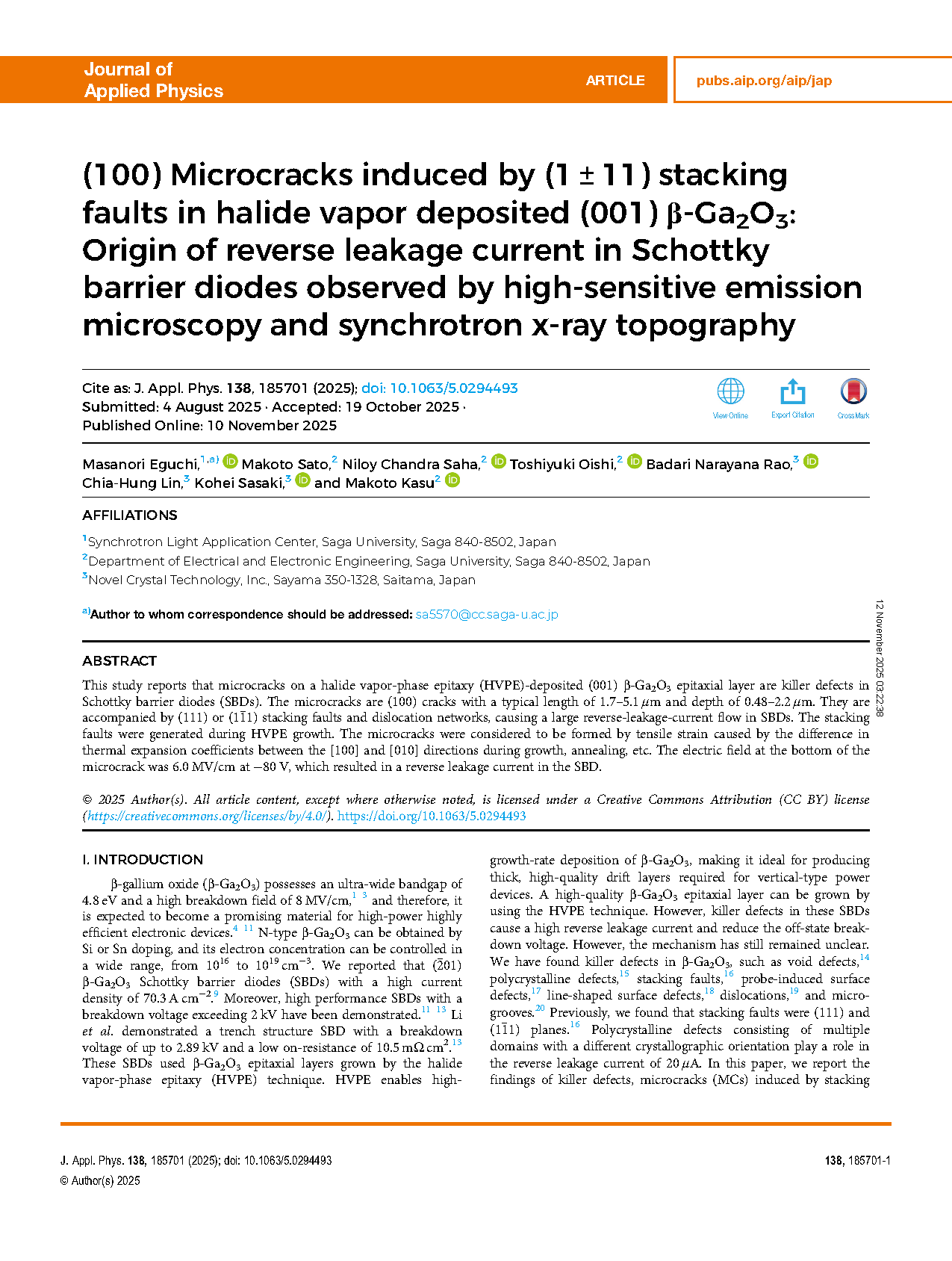
FIG. 1.I–V characteristics of squircle SBDs #C0732 (red) and #G0332 (blue) with the same width of 3200 μm (the area of 1.01 × 10⁻¹ cm2) on the same wafer.
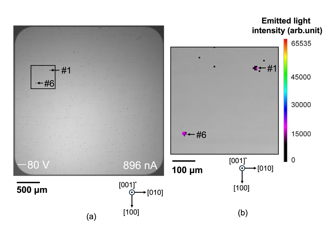
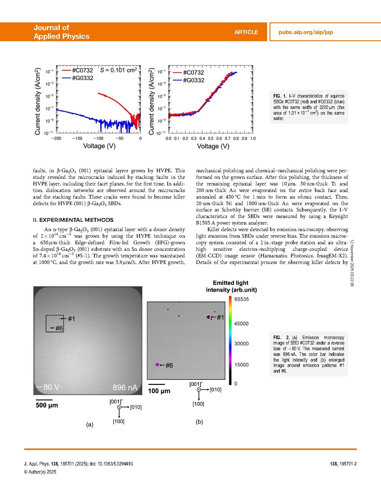
FIG. 2. (a) Emission microscopy image of SBD #C0732 under a reverse bias of −80 V. The measured current was 896 nA. The color bar indicates the light intensity and (b) enlarged image around emission patterns #1 and #6.

FIG. 3. X-ray topography image of SBD #C0732 obtained for g = 225. Aligned defects were observed as shown by arrows.
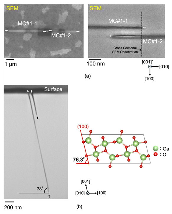
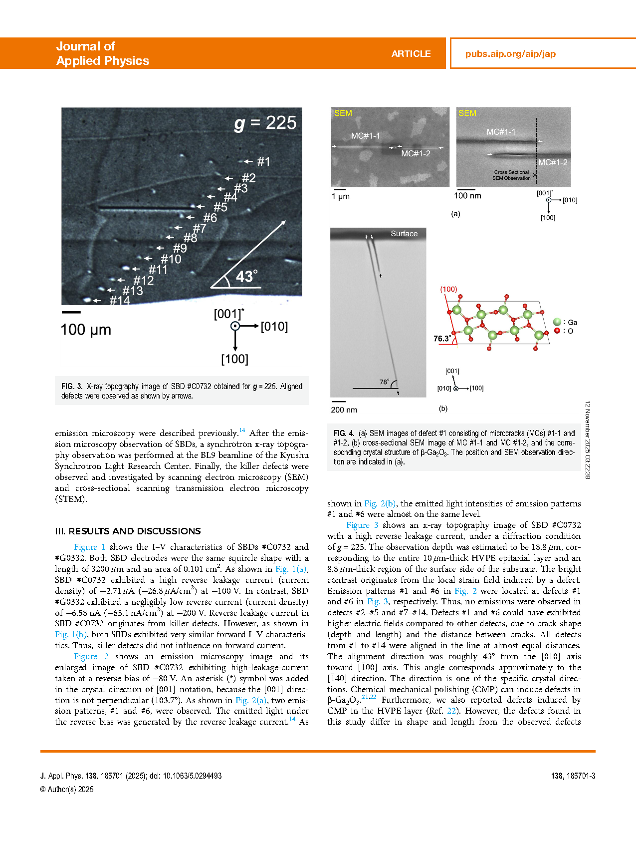
FIG. 4. (a) SEM images of defect #1 consisting of microcracks (MCs) #1-1 and #1-2, (b) cross-sectional SEM image of MC #1-1 and MC #1-2, and the corresponding crystal structure of β-Ga2O3. The position and SEM observation direction are indicated in (a).
FIG. 5. (a) SEM image of the SEM image of defect #6, (b) cross-sectional STEM image of MC #6-1. The position and STEM observation direction are indicated in Fig (a).
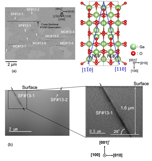
FIG. 6. (a) SEM image of defect #13 and the crystal structure of β-Ga2O3, (b) cross-sectional STEM image of SFs #13-1 and #13-2. The position and STEM observation direction are indicated in (a) and (c) cross-sectional STEM image of SF #13-1 rotated 12.6° counterclockwise around the [001]* axis and the corresponding crystal structure of β-Ga2O3 rotated 14° counterclockwise, (d) cross-sectional STEM image of SF #13-2 rotated 14.5° clockwise around the [001]* axis and the corresponding crystal structure of β-Ga2O3 rotated 14° clockwise.
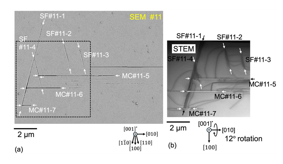
FIG. 7. (a) SEM image of defect #11 and (b) STEM bright field image of defect #11 for the counterclockwise rotation 12° around the [010] axis.
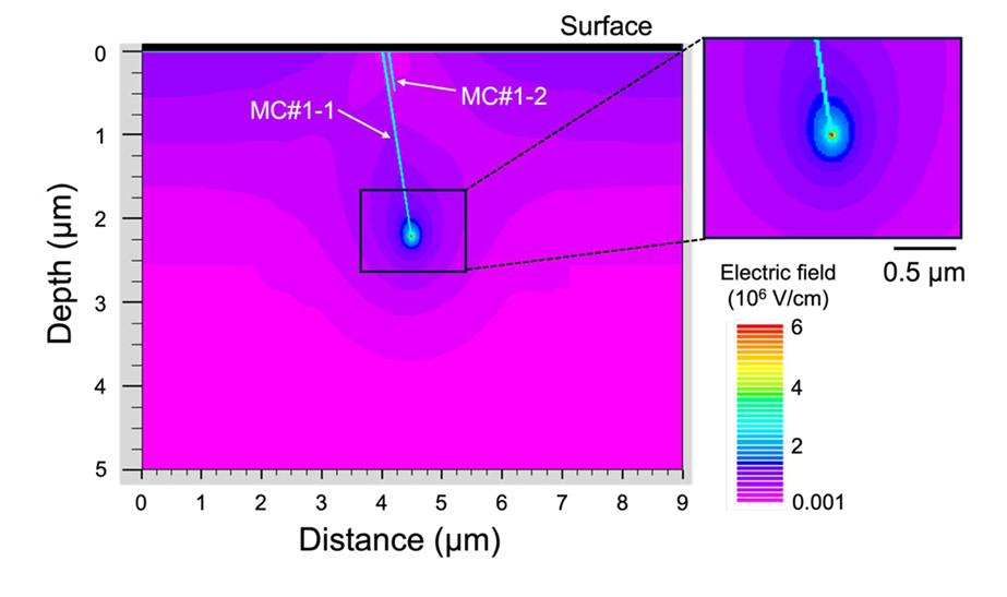
FIG. 8. Simulated electric field distribution of the cross section of MC #1 under a reverse bias of −80 V.
DOI:
doi.org/10.1063/5.0294493