Paper Sharing
【Member Papers】Investigation of electrical transport mechanisms in p-NiO/n-Ga₂O₃ junction barrier Schottky diodes with low leakage and high breakdown voltage
日期:2025-11-12阅读:478
Researchers from the Beijing University of Posts and Telecommunications and Nanjing University of Posts and Telecommunications have published a dissertation titled "Investigation of electrical transport mechanisms in p-NiO/n-Ga2O3 junction barrier Schottky diodes with low leakage and high breakdown voltage" in Physica Scripta.
Project Support
This work was supported by the National Key Research and Development Program of China (Grant 2022YFB3605404), the Joint Funds of the National Natural Science Foundation of China (Grant U23A20349), the Natural Science Foundation of Jiangsu Province (Grant BK20250657), and the Natural Science Research Start-up Foundation of Recruiting Talents of Nanjing University of Posts and Telecommunications (Grant XK1180924052).
Background
Future advancements in power electronic devices demand low power loss, large current density, and superior voltage with stand capability. Ga2O3 exhibits great potential for high-voltage and high-power electronic applications owing to its ultrawide bandgap (4.4–5.3 eV), high critical electric field strength (∼8 MV cm−1), excellent thermodynamic and structural stability, and a Baliga’s figure of merit(BFOM) exceeding 3000 relative to silicon (Si). These properties are superior to conventional semiconductors such as Si, silicon carbide (SiC), and gallium nitride (GaN). Furthermore, the low-cost substrate growth method and the availability of large-sized substrates have enabled Ga2O3 to become a promising candidate for next-generation commercial large-scale power semiconductor material. The electric field concentration at the sharp corners of the Schottky metal contact induces local field accumulation, resulting in intensified peak field strength and earlier breakdown at these regions. Extensive efforts have been devoted to developing high-performance Ga2O3-based SBDs, employing techniques such as field plates, dielectrics layer, and junction termination extensions to effectively suppress peak electric fields.
Abstract
High-performance gallium oxide (Ga2O3) junction barrier Schottky (JBS) diodes were fabricated using planar and trench junction barrier designs. Their electrical transport mechanisms were systematically studied. The JBS integration strengthens interfacial depletion via p–n junction-induced Ga2O3 conduction band elevation, whereas the trench design forms a higher interfacial barrier and expands lateral depletion, effectively modulating carrier transport. Additionally, the JBS structure reduces the electric field at the Schottky interface which not only suppresses Schottky barrier lowering to reduce reverse leakage current but also mitigates surface field crowding to prevent premature device breakdown. The forward current density ratios of Schottky barrier diodes (SBDs) with a JBS reached an impressive 8.0 × 10¹⁰, demonstrating exceptional switching characteristics. The reverse breakdown voltage of the SBDs with trench JBS increases from 310 V in the SBDs to a remarkable 1150 V, representing roughly a 3.7-time. The leakage current is simultaneously reduced by two orders of magnitude to an ultra-low value of 1.1 × 10⁻⁹ A cm−2. A comparative analysis of device performance between planar and trench JBS structures is presented, offering a theoretical foundation and reference for future innovations in Ga2O3-based SBDs.
Conclusions
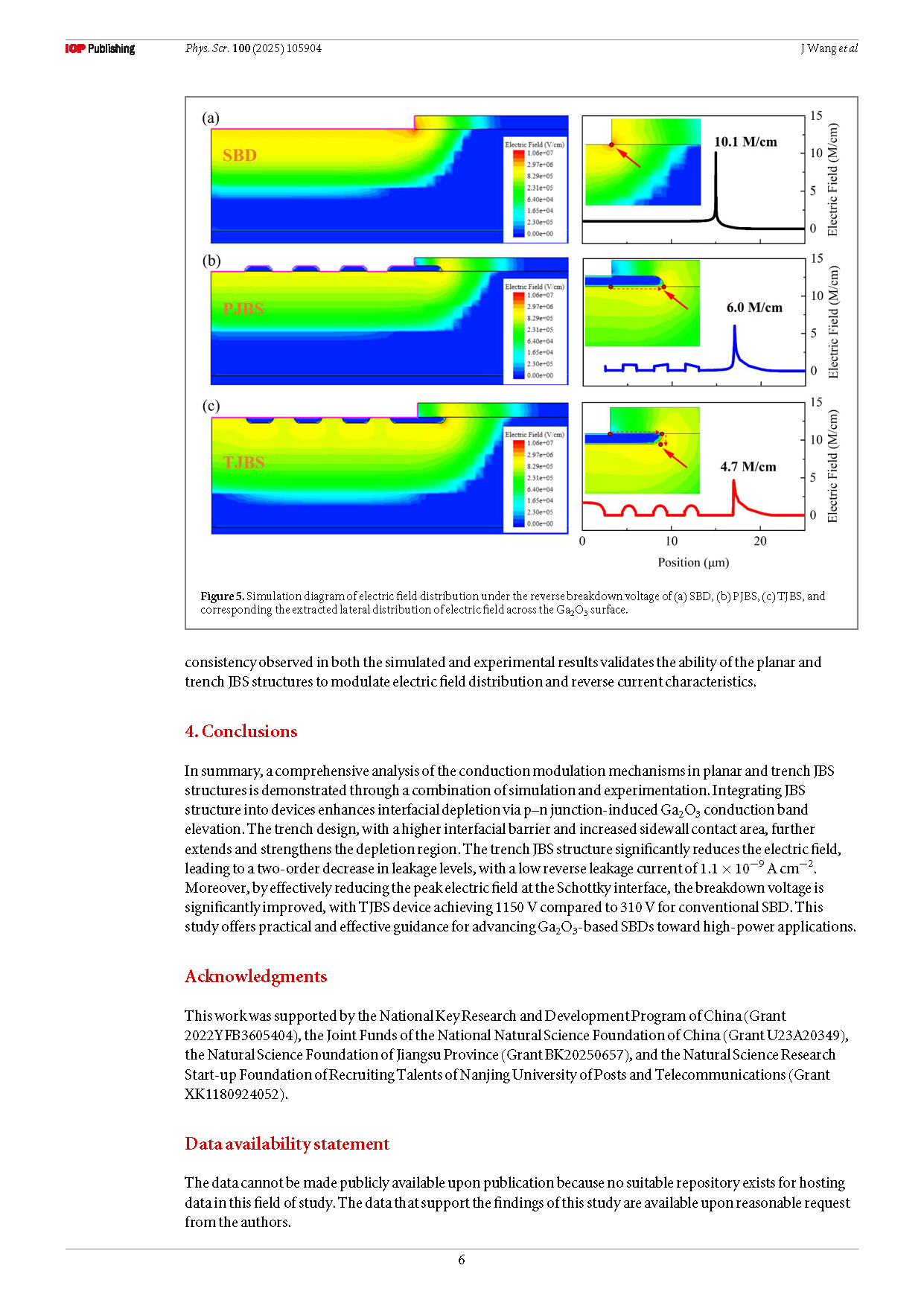
In summary, a comprehensive analysis of the conduction modulation mechanisms in planar and trench JBS structures is demonstrated through a combination of simulation and experimentation. Integrating JBS structure into devices enhances interfacial depletion via p–n junction-induced Ga2O3 conduction band elevation. The trench design, with a higher interfacial barrier and increased sidewall contact area, further extends and strengthens the depletion region. The trench JBS structure significantly reduces the electric field, leading to a two-order decrease in leakage levels, with a low reverse leakage current of 1.1 ×10⁻⁹A cm−2. Moreover, by effectively reducing the peak electric field at the Schottky interface, the breakdown voltage is significantly improved, with TJBS device achieving 1150 V compared to 310 V for conventional SBD. This study offers practical and effective guidance for advancing Ga2O3-based SBDs toward high-power applications.
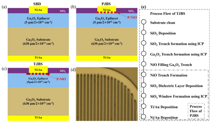
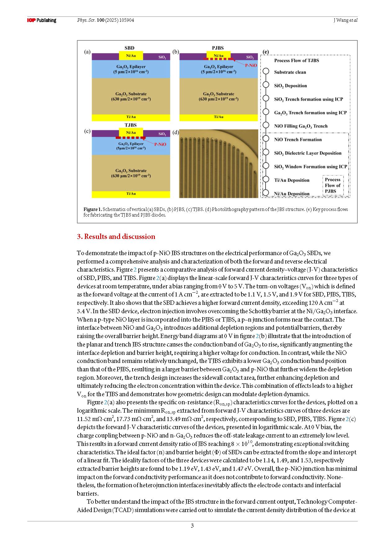
Figure 1. Schematics of vertical (a) SBDs, (b) PJBS, (c) TJBS. (d) Photolithography pattern of the JBS structure. (e)Key process flows for fabricating the TJBS and PJBS diodes.
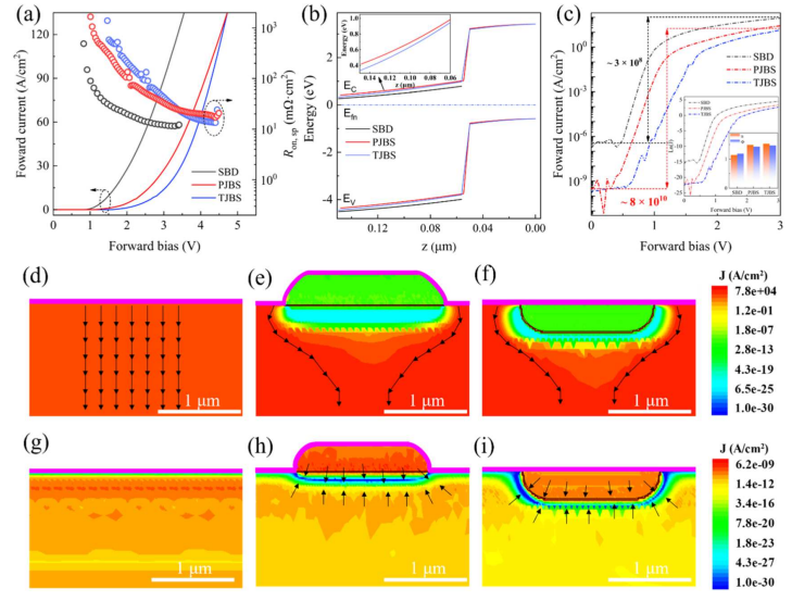
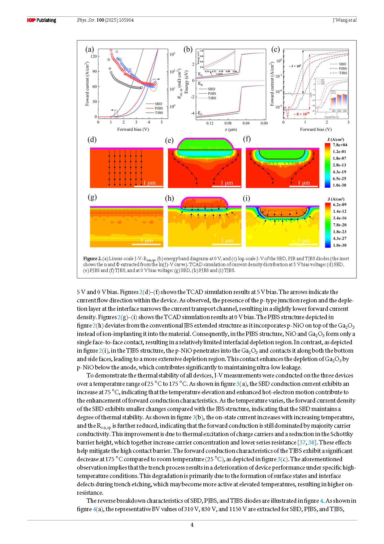
Figure 2. (a) Linear-scale J-V-Ron,sp, (b) energy band diagrams at 0 V, and (c) log-scale J-V of the SBD, PJB and TJBS diodes (the inset shows the n and Φ extracted from the ln(J)-V curve). TCAD simulation of current density distribution at 5 V bias voltage:(d) SBD, (e) PJBS and (f) TJBS, and at 0 V bias voltage: (g) SBD, (h) PJBS and (i) TJBS.
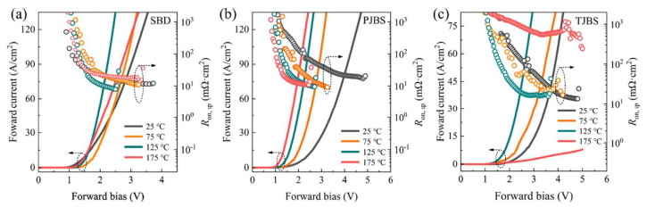
Figure 3. Temperature-dependent J-V characteristics of(a) SBDs, (b) PJBS, and (c) TJBS.
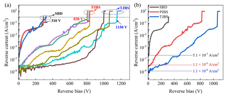
Figure 4. Breakdown characteristics of the three device structures with (a) inverse J-V curve, (b)representative coordinate-inverse J-V curve.
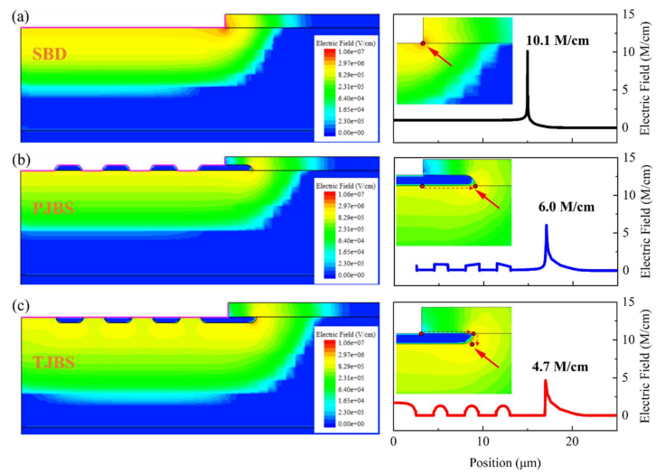
Figure 5. Simulation diagram of electric field distribution under the reverse breakdown voltage of (a) SBD, (b) PJBS, (c) TJBS, and corresponding the extracted lateral distribution of electric field across the Ga2O3 surface.
DOI:
doi.org/10.1088/1402-4896/ae098a