Paper Sharing
【Domestic Papers】The Effect of Thickness on the Optoelectronic Properties of Zn doped β-Ga₂O₃ Thin Films
日期:2025-11-12阅读:464
Researchers from the Shanghai Dianji University have published a dissertation titled "The Effect of Thickness on the Optoelectronic Properties of Zn doped β-Ga2O3 Thin Films" in Physica B: Condensed Matter.
Project Support
This work was financially supported by the National Natural Science Foundation of China (Grant No. U22A2073).
Background
As an emerging ultra-wide bandgap (UWBG) semiconductor with a bandgap of ~4.9 eV, β-Ga₂O₃ has attracted extensive interest for its potential applications in power electronics and deep-ultraviolet (DUV) optoelectronics due to its ultrahigh breakdown electric field (8 MV/cm), excellent thermal and chemical stability, and strong sensitivity to the solar-blind ultraviolet (SBUV, 200–280 nm) spectrum. However, achieving stable p-type β-Ga₂O₃ remains a major challenge, primarily hindered by intrinsic defects such as oxygen vacancies, the lack of effective p-type dopants, a flat valence band maximum dominated by O 2p orbitals, and severe hole self-trapping effects. Previous studies have demonstrated that Zn doping can effectively modify the electronic structure and defect states of β-Ga₂O₃, forming shallow acceptor levels and suppressing oxygen vacancies, thereby improving its optoelectronic performance. Both theoretical and experimental results indicate that Zn incorporation can modulate lattice strain, enhance rectification behavior, and offer a feasible approach to p-type β-Ga₂O₃. Nevertheless, the influence of film thickness on the structural, strain, defect, and electrical properties of Zn-doped β-Ga₂O₃ remains insufficiently explored. In this work, Zn-doped β-Ga₂O₃ films were epitaxially grown on c-plane sapphire substrates via pulsed laser deposition (PLD), and the thickness-dependent optoelectronic and rectification behaviors of β-Ga₂O₃:Zn films and β-Ga₂O₃/β-Ga₂O₃:Zn heterojunctions were systematically investigated. This study provides new insights into resolving the long-standing p-type instability issue through thickness-optimized defect passivation and strain control, paving the way for high-performance solar-blind ultraviolet photodetectors.
Abstract
We systematically investigate thickness-dependent properties of Zn-doped β-Ga2O3 films (20–182 nm) epitaxially grown on c-sapphire via pulsed laser deposition. Enhanced crystallinity, reduced interfacial strain (XRD FWHM: 0.910°→0.788°), and increased grain height (1.3 → 18.3 nm) were observed with thickness. Electrical measurements show improved mobility (1.13 → 1.63 cm2 V−1 s−1) and decreased resistivity, though bulk conduction remains n-type. Optical bandgap widens significantly (4.75 → 5.00 eV) due to compressive strain relaxation. Cathodoluminescence confirms Zn-mediated suppression of deep-level defects. Crucially, the β-Ga2O3/β-Ga2O3: Zn heterojunction exhibits rectifying behavior (turn-on: 5.1 V), demonstrating interface-induced p-type conductivity despite n-type bulk. This work resolves p-type instability challenges via thickness-optimized defect passivation and strain control for solar-blind UV photodetectors.
Highlights
● Thickness increase reduces strain and promotes grain growth, optimizing structure.
● Electrical properties improve with higher mobility and lower resistivity.
● Bandgap widening enables tunable optical absorption for UV applications.
● Defect suppression via oxygen vacancy passivation enhances emission.
● Heterojunction shows rectifying behavior, demonstrating interface p-type conductivity.
Conclusion
This study elucidates the profound impact of film thickness on the optoelectronic performance of Zn-doped β-Ga₂O₃ thin films. Increasing growth duration (10–90 min) enhances crystallinity, reduces residual strain, and promotes vertical grain growth (height: 1.3 → 18.3 nm), leading to improved electrical properties, including reduced resistivity (3.81 × 10⁶ Ω·cm) and higher carrier mobility (1.63 cm²·V⁻¹·s⁻¹). The observed bandgap expansion (4.75 → 5.00 eV) and suppressed defect-related emissions in thicker films confirm effective Zn-mediated oxygen vacancy passivation. Critically, while bulk electrical characterization indicated n-type dominance, the β-Ga₂O₃/β-Ga₂O₃:Zn heterojunction exhibited clear rectifying behavior (turn-on: 5.1 V), demonstrating interface-mediated p-type functionality. Most significantly, although Zn doping did not achieve bulk p-type conductivity due to compensation, it successfully created acceptor states that enabled distinct rectification in the β-Ga₂O₃/β-Ga₂O₃:Zn heterojunction. This demonstrates that interface-induced p-type functionality is a viable and effective strategy for realizing solar-blind photodetectors, circumventing the longstanding challenge of bulk p-type conduction in β-Ga₂O₃. The thickness-dependent approach effectively resolves interfacial strain challenges and enables functional heterojunction devices, accelerating their deployment in solar-blind UV detection applications.
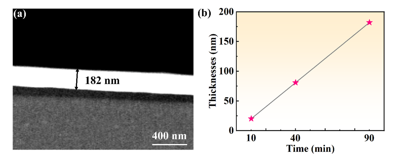
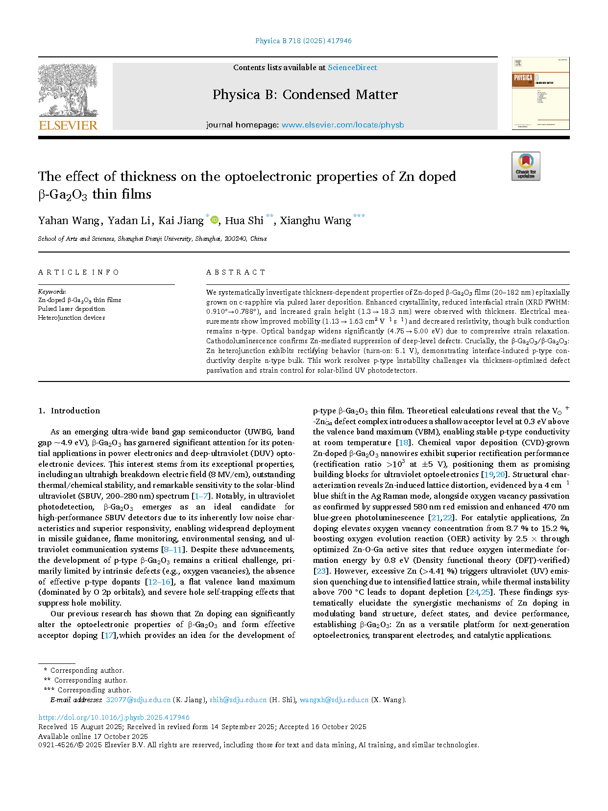
Fig. 1. (a) Cross-sectional SEM image of Zn-doped β-Ga2O3 thin film grown for 90 min. (b) The thicknesses of the 10-min and 40-min films were estimated by linear fitting based on the thickness of the 90-min film.

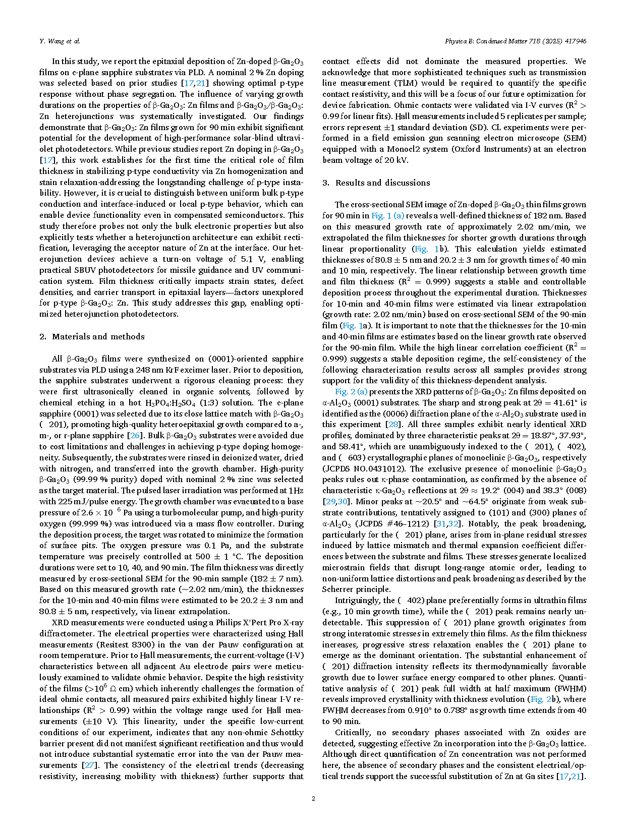
Fig. 2. (a) XRD patterns of Zn-doped β-Ga2O3 thin films grown for 10 min, 40 min, and 90 min. (b) β-Gallium oxide (-201) diffraction peak attenuation map. (c) D-spacing calculated from the (-201) diffraction peak.

Fig. 2. (a) XRD patterns of Zn-doped β-Ga2O3 thin films grown for 10 min, 40 min, and 90 min. (b) β-Gallium oxide (-201) diffraction peak attenuation map. (c) D-spacing calculated from the (-201) diffraction peak.
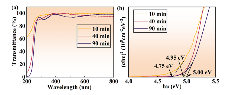
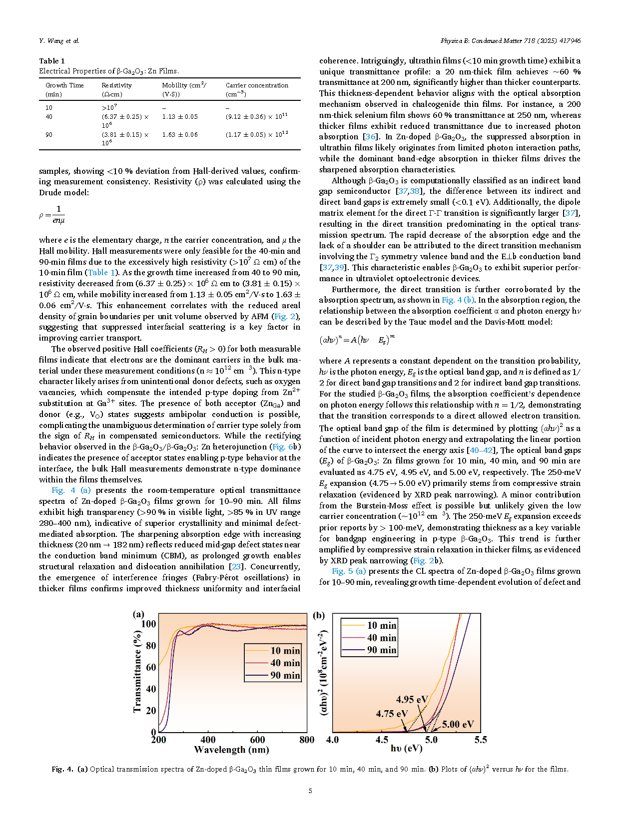
Fig. 4. (a) Optical transmission spectra of Zn-doped β-Ga2O3 thin films grown for 10 min, 40 min, and 90 min. (b) Plots of (αhν)2 versus hν for the films.

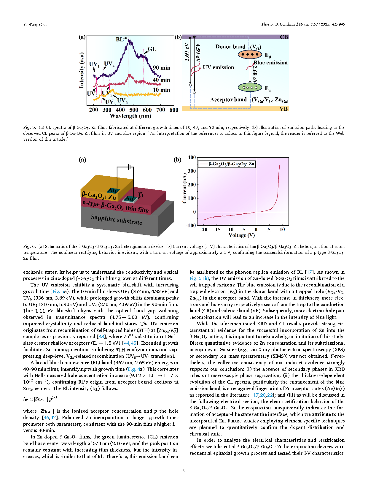
Fig. 5. (a) CL spectra of β-Ga2O3: Zn films fabricated at different growth times of 10, 40, and 90 min, respectively. (b) Illustration of emission paths leading to the observed CL peaks of β-Ga2O3: Zn films in UV and blue region. (For interpretation of the references to colour in this figure legend, the reader is referred to the Web version of this article.)
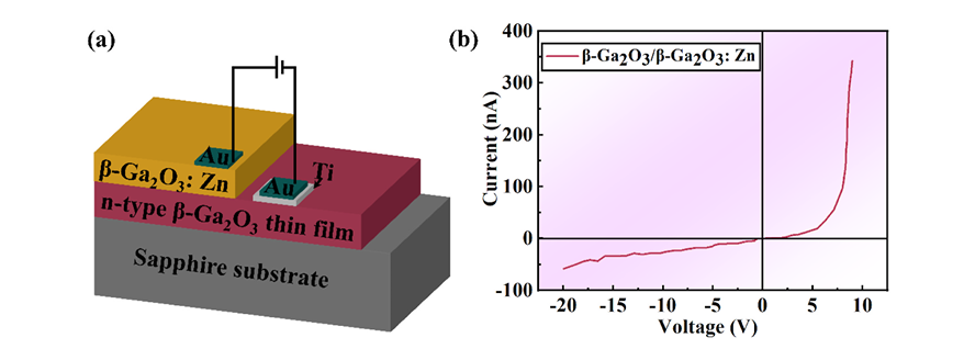
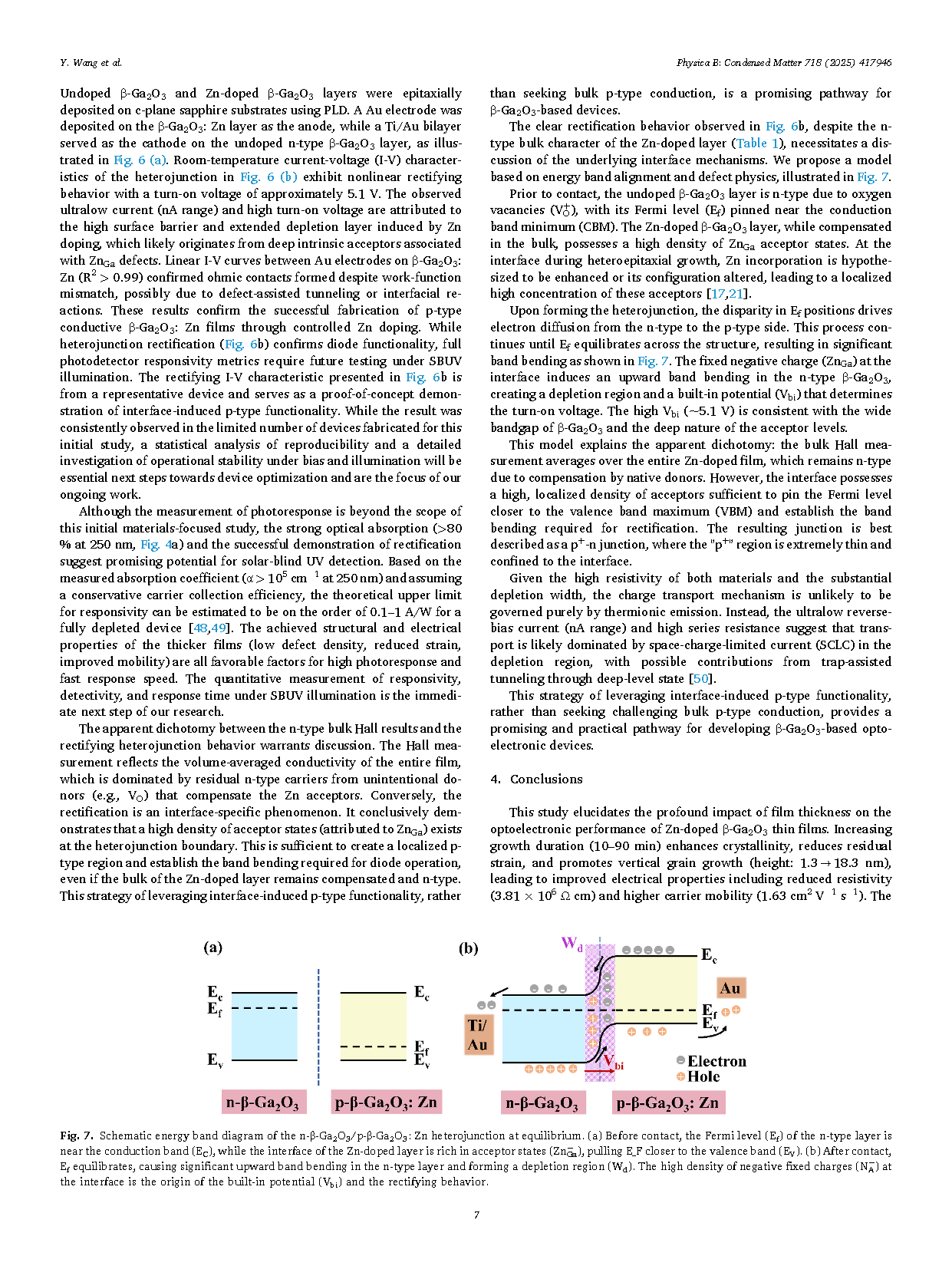
Fig. 6. (a) Schematic of the β-Ga2O3/β-Ga2O3: Zn heterojunction device. (b) Current-voltage (I–V) characteristics of the β-Ga2O3/β-Ga2O3: Zn heterojunction at room temperature. The nonlinear rectifying behavior is evident, with a turn-on voltage of approximately 5.1 V, confirming the successful formation of a p-type β-Ga2O3: Zn film.
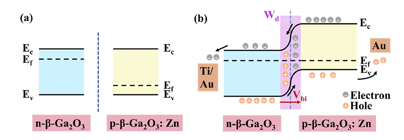
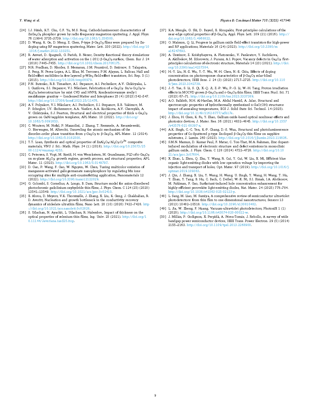
Fig. 7. Schematic energy band diagram of the n-β-Ga2O3/p-β-Ga2O3: Zn heterojunction at equilibrium. (a) Before contact, the Fermi level (Ef) of the n-type layer is near the conduction band (EC), while the interface of the Zn-doped layer is rich in acceptor states (ZnGa), pulling E_F closer to the valence band (EV). (b) After contact, Ef equilibrates, causing significant upward band bending in the n-type layer and forming a depletion region (Wd). The high density of negative fixed charges (NA) at the interface is the origin of the built-in potential (Vbi) and the rectifying behavior.
DOI:
doi.org/10.1016/j.physb.2025.417946