Paper Sharing
【Member Papers】Heteroepitaxial growth of β-Ga₂O₃ thin films on Si (111) substrates via interfacial engineering for self-powered ultraviolet photodetectors
日期:2025-11-11阅读:455
Researchers from the Sichuan Normal University have published a dissertation titled "Heteroepitaxial growth of β-Ga2O3 thin films on Si (111) substrates via interfacial engineering for self-powered ultraviolet photodetectors" in Applied Surface Science.
Project Support
The authors acknowledge the Ion Beam Center (IBC) at Helmholtz-Zentrum Dresden-Rossendorf (HZDR) for performing the ion beam analysis. T. W. thanks Muyuan Zhao from Zolix for his assistance in photoresponse measurements. M. W. thanks Ilona Skorupa for her assistance in pulsed laser deposition. This work is funded by the National Natural Science Foundation of China (NSFC) (grant No. 12575311, and 12205212) and the Natural Science Foundation of Sichuan Province (NSFSC) (grant No. 24NSFSC1355).
Background
The beta-phase gallium oxide (β-Ga2O3) has fascinating properties, e.g. superior thermo-dynamical stability and ultrawide bandgap of 4.5–4.9 eV, which results in a breakdown electrical field of as high as 8 MV/cm, eventually leading to large Baliga’s figure of merit over other wide-band semiconductors such as 4H-SiC and GaN. Moreover, there is growing interest in β-Ga2O3 for prospective applications in ultraviolet (UV) photodetectors, gas sensors, X-ray detectors and high-power microwave and radio frequency devices. Particularly, the heteroepitaxial growth of β-Ga2O3 thin films on technology relevant substrates is essential for breaking cost and integration barriers, which broadens the market for β-Ga2O3-based devices, towards monolithic integration of UV-bandgap optoelectronics, power devices as well as β-Ga2O3-based metal–oxide–semiconductor field-effect transistors (MOSFETs).
Abstract
β-Ga2O3 holds great promises for solar-blind ultraviolet photodetection and energy-efficient electronic electronics. Overcoming the lattice and thermal mismatch in heteroepitaxial growth on Si is critical to achieving complementary metal–oxide–semiconductor (CMOS)-compatible and cost-effective devices. In this work, we demonstrate the AlN-mediated heteroepitaxial growth of β-Ga2O3 thin films on Si (111) substrate via pulsed laser deposition. We systematically investigate the influence of key growth parameters, specifically temperature and oxygen pressure, on the film crystallinity, demonstrating that optimized conditions effectively reduce defects and improve phase purity. Comprehensive structural and chemical analysis reveals that the optimized films exhibit strong Ga-O bonding, near-stoichiometric composition, high visible transparency, and a sharp ultraviolet (UV) absorption edge. Prototype solar blind photodetectors based on the β-Ga2O3/AlN/Si film display self-powered photoresponse and favorable optoelectronic characteristics, promising for real-time UV monitoring in harsh environments. These results provide a fundamental understanding and a practical, scalable route for integrating β-Ga2O3 with mainstream Si technology, paving the way for advanced, energy-efficient optoelectronic and power electronic devices.
Highlights
● AlN buffer layer enables heteroepitaxial growth of β-Ga2O3 thin films on Si (111).
● Optimized PLD parameters achieve high-phase-purity and low-defect β-Ga2O3 films.
● Strong Ga-O bonding and near-stoichiometry enhance optical quality of β-Ga2O3 films.
● β-Ga2O3 films exhibit sharp UV cutoff (∼270 nm) and high solar-blind selectivity.
● Self-powered solar-blind photodetector fabricated on CMOS-compatible Si platform.
Conclusion
In summary, we have displayed a systematic investigation on the heteroepitaxial growth of β-Ga2O3 films on Si (111) substrate using PLD. The strategic incorporation of an AlN (002) interlayer effectively mitigated the lattice mismatch between β-Ga2O3 and the Si (111) substrate, resulting in the heteroepitaxial β-Ga2O3/AlN/Si (111) films. We have found the β-Ga2O3/AlN/Si (111) films are highly oriented heteroepitaxial growth with low-angle grain boundaries, which exhibits an orientation of (−201) and a relatively low RMS values of around 3 nm. Moreover, we demonstrate that the β-Ga2O3/AlN/Si (111) films exhibit an absorption edge spanning 230–310 nm, corresponding to tunable bandgap energies of 4.6–4.8 eV. In addition, we fabricated solar-blind UV detectors based on the β-Ga2O3/AlN/Si (111) films in MSM structure, which exhibits self-powered operation capabilities, showcasing reasonable photoresponse characteristics that directly correlate with enhanced material properties. This work establishes a solution for the heteroepitaxial growth of β-Ga2O3 on Si, advancing cost-effective fabrication methodologies for β-Ga2O3 thin films with structural integrity and optoelectronic properties applicable in next-generation power electronics and deep-ultraviolet photonic devices.
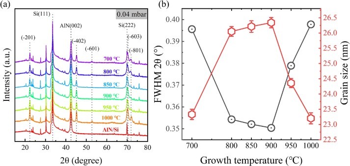
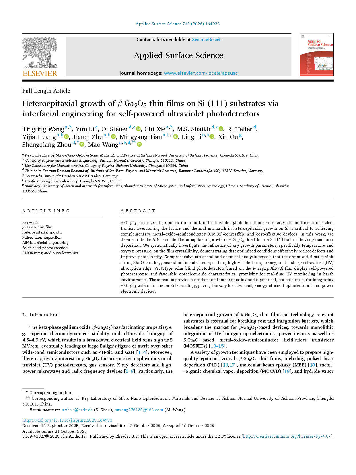
Fig. 1. The structural properties characterizations for β-Ga2O3/AlN/Si (111) samples. (a) XRD θ-2θ patterns for the β-Ga2O3 films at the growth temperature of 700–1000 °C with fixed oxygen pressure of 0.04 mbar. (b) FWHM of the (−201) peak and grain size as a function of growth temperature.

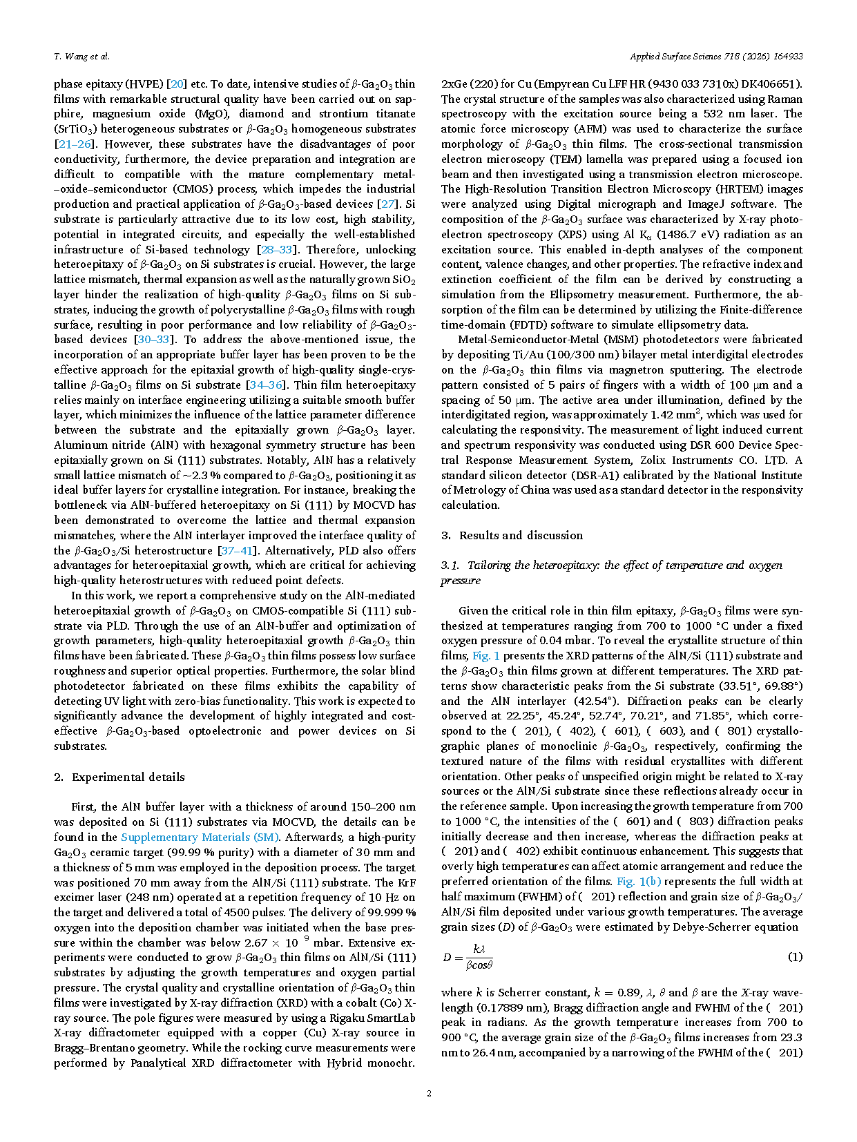
Fig. 2. The structural properties characterizations for β-Ga2O3/AlN/Si (111) samples. (a)-(c) the XRD θ-2θ diffraction patterns of β-Ga2O3 films grown under varying oxygen pressures at 800 °C, 850 °C, and 900 °C, respectively. (d)-(f) The temperature-dependent evolution of the FWHM of (−201) reflection, and grain size for β-Ga2O3 films deposited at these three temperatures.
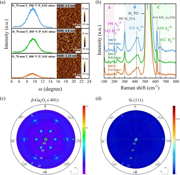
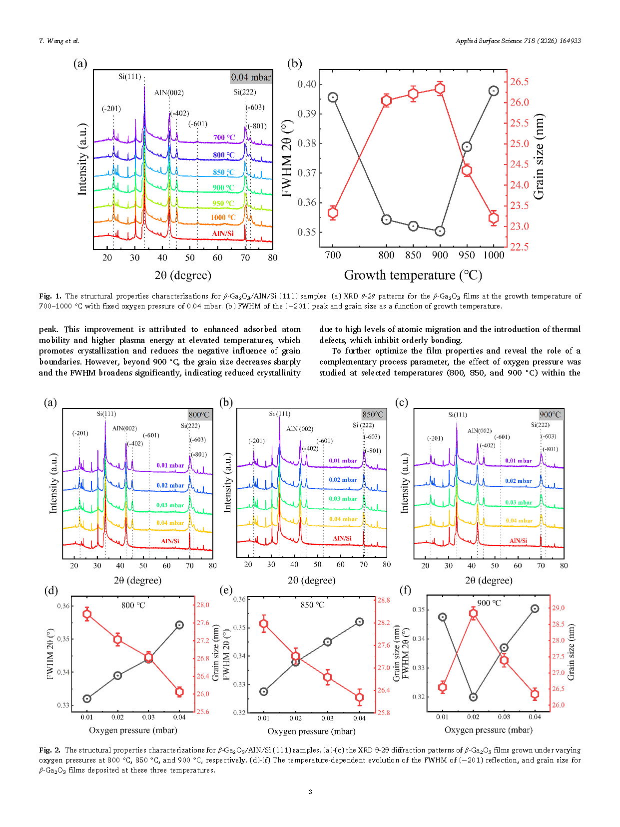
Fig. 3. (a) The rocking curve of β-Ga2O3 (−201) plane and AFM images of β-Ga2O3 films. (b) Raman spectra of β-Ga2O3/AlN/Si (111) samples. (c) The pole figure from (−401) for β-Ga2O3/AlN/Si (111) film. (d) The poles figure from Si (111) for the substrate. The azimuthal angle β and the polar angle α (α = 90-χ) of pole figures were measured from 0° to 360° and from 15° to 90°, respectively.
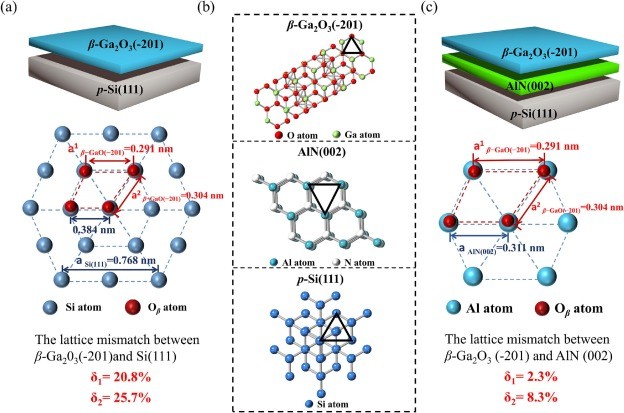
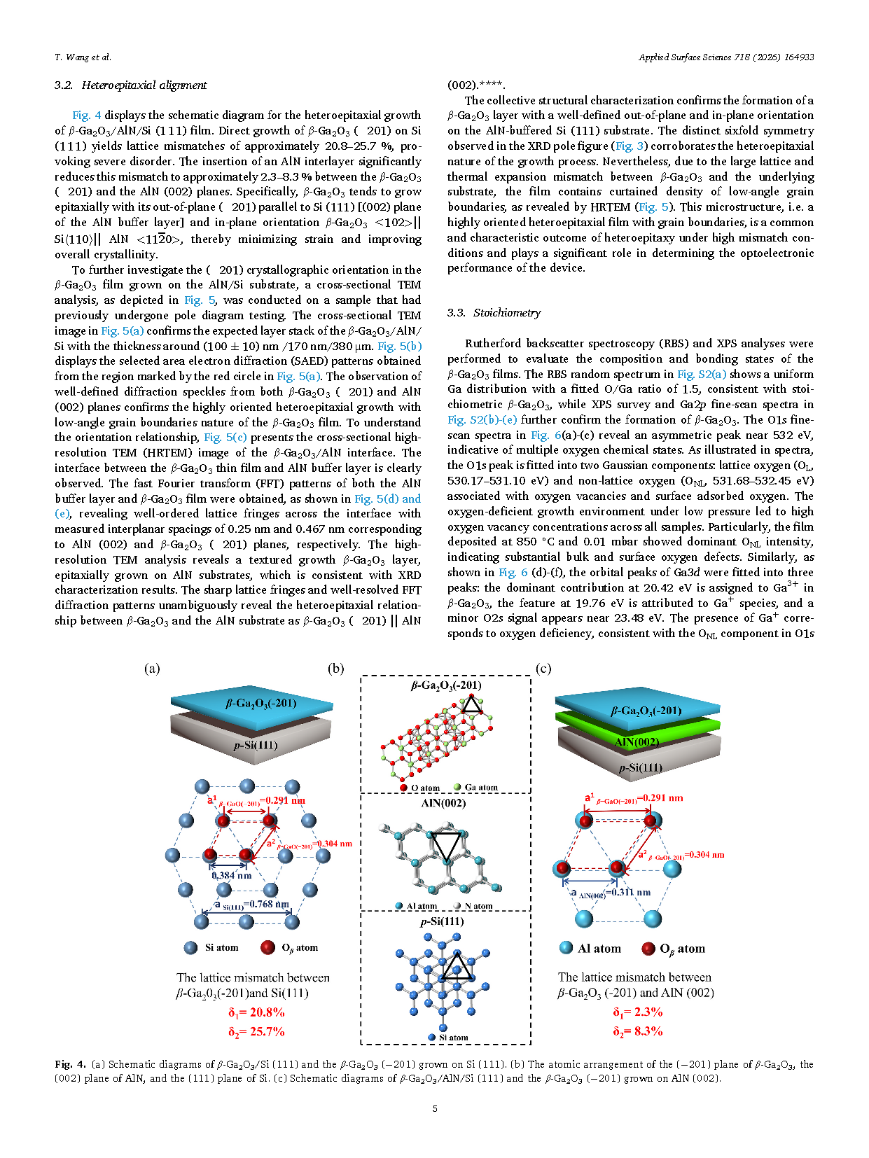
Fig. 4. (a) Schematic diagrams of β-Ga2O3/Si (111) and the β-Ga2O3 (−201) grown on Si (111). (b) The atomic arrangement of the (−201) plane of β-Ga2O3, the (002) plane of AlN, and the (111) plane of Si. (c) Schematic diagrams of β-Ga2O3/AlN/Si (111) and the β-Ga2O3 (−201) grown on AlN (002).
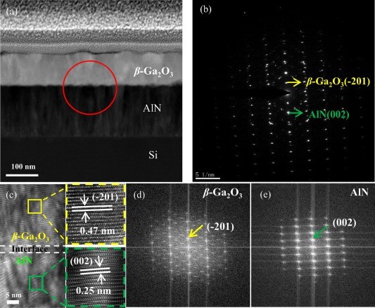
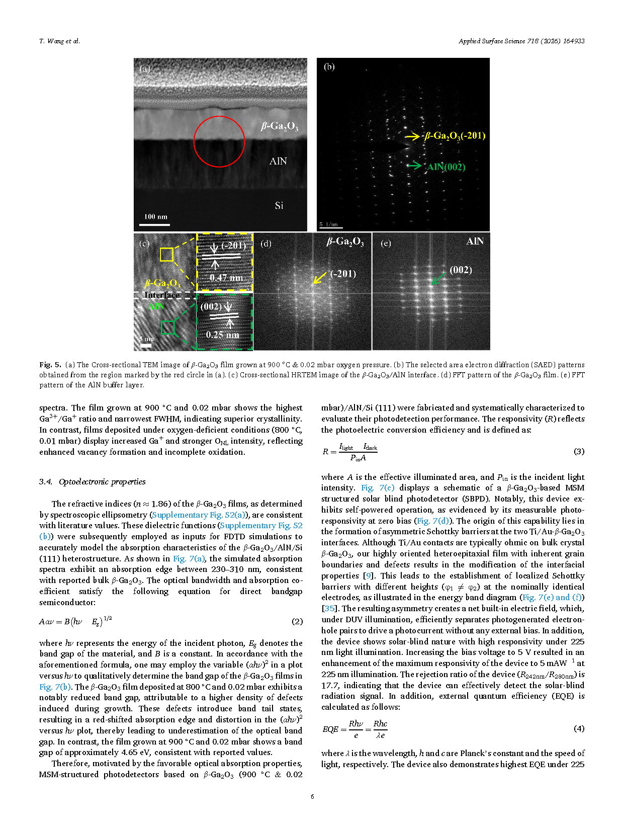
Fig. 5. (a) The Cross-sectional TEM image of β-Ga2O3 film grown at 900 °C & 0.02 mbar oxygen pressure. (b) The selected area electron diffraction (SAED) patterns obtained from the region marked by the red circle in (a). (c) Cross-sectional HRTEM image of the β-Ga2O3/AlN interface. (d) FFT pattern of the β-Ga2O3 film. (e) FFT pattern of the AlN buffer layer.
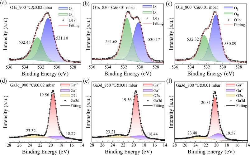
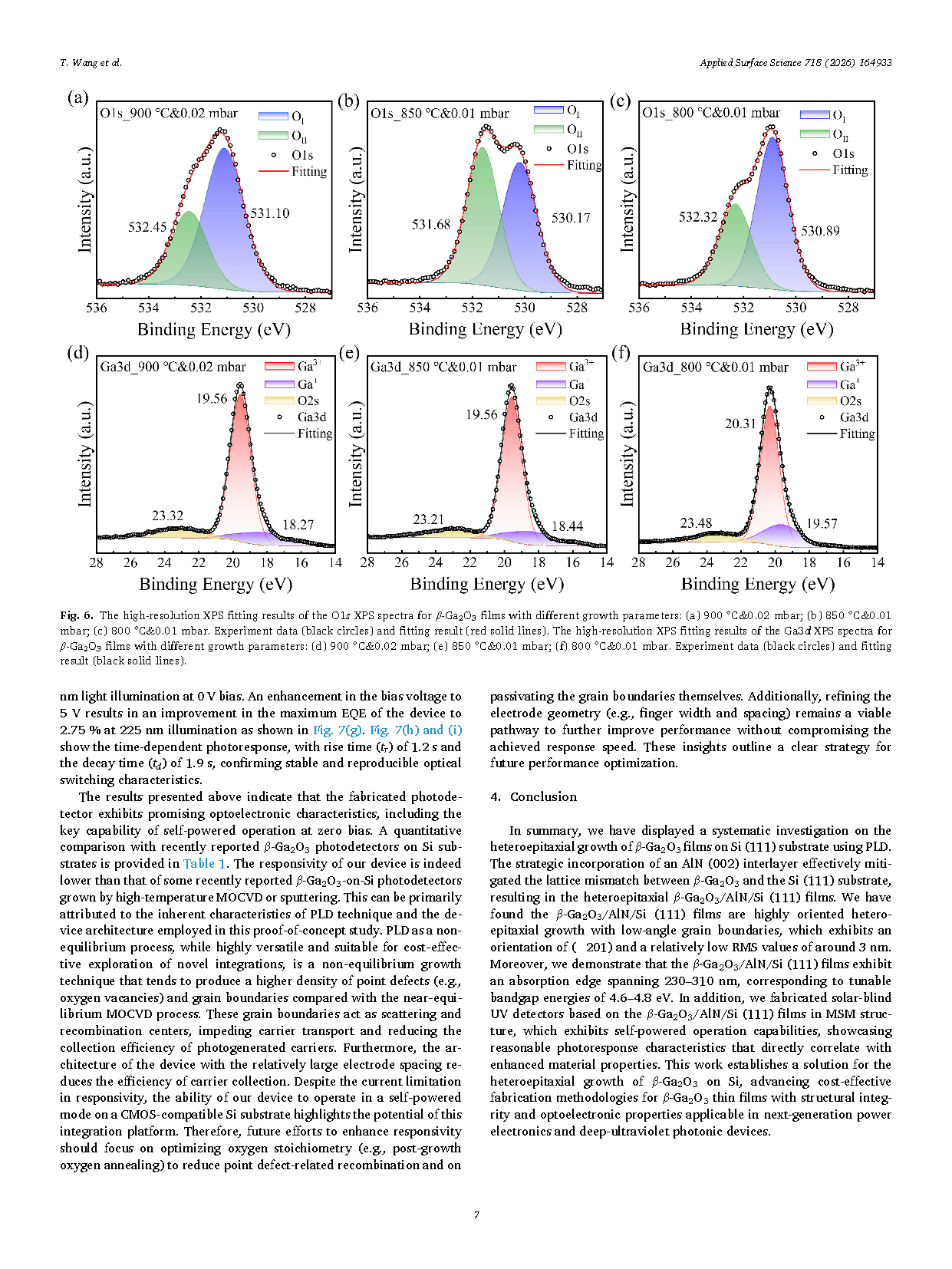
Fig. 6. The high-resolution XPS fitting results of the O1s XPS spectra for β-Ga2O3 films with different growth parameters: (a) 900 °C&0.02 mbar; (b) 850 °C&0.01 mbar; (c) 800 °C&0.01 mbar. Experiment data (black circles) and fitting result (red solid lines). The high-resolution XPS fitting results of the Ga3d XPS spectra for β-Ga2O3 films with different growth parameters: (d) 900 °C&0.02 mbar; (e) 850 °C&0.01 mbar; (f) 800 °C&0.01 mbar. Experiment data (black circles) and fitting result (black solid lines).
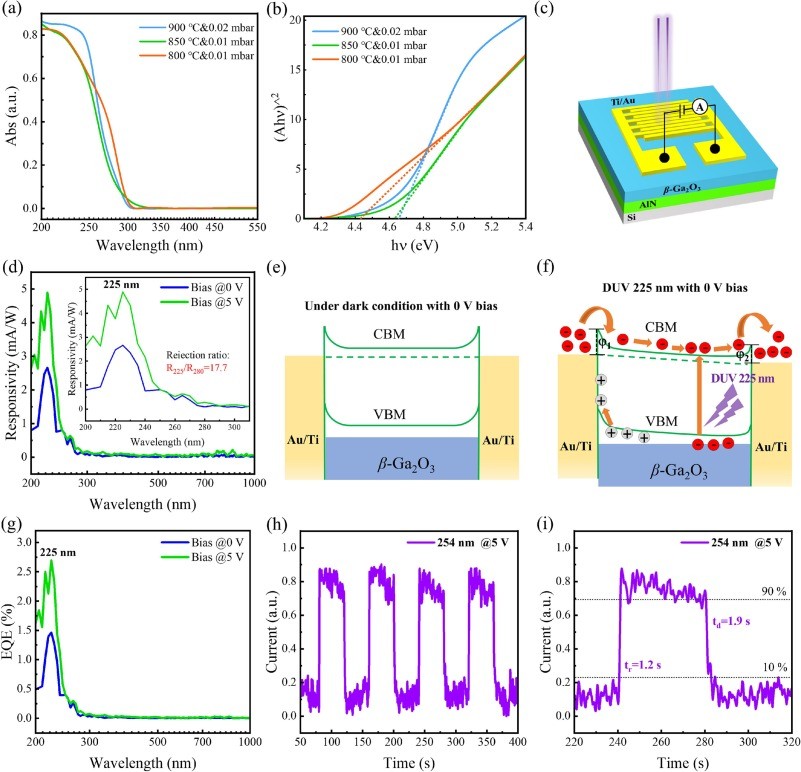
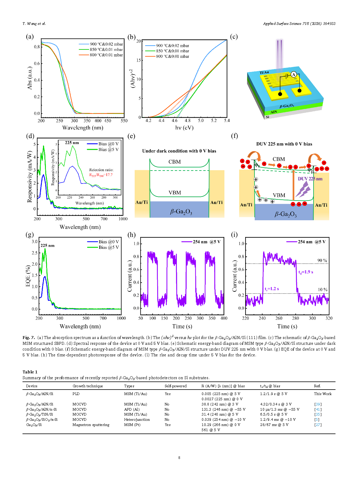
Fig. 7. (a) The absorption spectrum as a function of wavelength. (b) The (αhν)2 versus hν plot for the β-Ga2O3/AlN/Si (111) film. (c) The schematic of β-Ga2O3-based MSM structured SBPD. (d) Spectral response of the device at 0 V and 5 V bias. (e) Schematic energy-band diagram of MSM type β-Ga2O3/AlN/Si structure under dark condition with 0 bias. (f) Schematic energy-band diagram of MSM type β-Ga2O3/AlN/Si structure under DUV 225 nm with 0 V bias. (g) EQE of the device at 0 V and 5 V bias. (h) The time-dependent photoresponse of the device. (i) The rise and decay time under 5 V bias for the device.
DOI:
doi.org/10.1016/j.apsusc.2025.164933